
 Open Access Article
 This Open Access Article is licensed under a Creative Commons Attribution-Non Commercial 3.0 Unported Licence
Improved interface passivation by optimizing a polysilicon film under different hydrogen dilution in N-type TOPCon silicon solar cells
Yanhong Huang,
Lizhe Jia,
Xiaomeng Shi,
Xiaoyu Liu,
Wanbing Lu,
Ridong Cong,
Chao Gao and
Wei Yu *
*
Hebei Key Laboratory of Optic-Electronic Information and Materials, National & Local Joint Engineering Laboratory of New Energy Photoelectric Devices, College of Physics Science and Technology, Hebei University, Baoding 071002, China. E-mail: yuwei@hbu.edu.cn
First published on 26th April 2022
Abstract
The passivation properties of a polysilicon (poly-Si) thin film are the key for improving the photovoltaic performance of TOPCon silicon solar cells. In this work, we investigate the influence of the poly-Si microstructure on the interface passivation and photovoltaic performance in TOPCon solar cells. The poly-Si thin films are prepared from phosphorus-doped hydrogenated microcrystalline silicon (μc-Si:H) layers deposited via plasma enhanced chemical vapor deposition (PECVD) under different hydrogen dilutions and recrystallized by high temperature post-deposition annealing. The results revealed that, as the hydrogen dilution ratio increases, the microstructure of the pre-deposited films transforms from an amorphous phase to a microcrystalline phase. Meanwhile, the effective minority carrier lifetime of the symmetrically passivated contact structure shows a maximum value of 1.75 ms, implying that the efficient passivation at the c-Si interface is obtained which is mainly attributed to the joint enhancement of the improved field effect passivation from poly-Si films and the reduced defects density on the silicon surface. Consequently, the devices displayed excellent rectification behavior with a rectifying ratio of 3 × 10⁵, ascribed to the enhanced carrier transport with the high quality poly-Si film pre-deposited in the initial region of structural transition. Correspondingly, the obvious improvement of TOPCon solar cell performance was achieved, exhibiting an optimized conversion efficiency of 17.91%. The results provide an optimal design scheme for enhancing the photovoltaic properties of the TOPCon silicon solar cells.
1. Introduction
Carrier recombination loss at the metal–semiconductor interface is the key to restricting the improvement of photoelectric conversion efficiency of silicon solar cells.1,2 Currently, the rear surface and metal contact in high efficiency silicon solar cells mostly adopt the localized contact structure (passivated emitter rear contact abbreviated as PERC) to reduce the contact areas. The efficiency of PERC silicon solar cells has reached 25% due to the significant suppression of the carrier recombination loss at the rear metal contact.3,4 However, reducing the contact area is limited by the printing accuracy and will increase the series resistance of the devices.2 Complex processes such as laser opening also hinder the lowering of production costs.5 The most important is that these localized contacts still suffer from high recombination. A poly-Si based passivated contact scheme is considered the most feasible solution for reducing the recombination losses in the surface and metalized area.6 Therefore, Tunnel Oxide Passivated Contact (TOPCon) silicon solar cells have attracted remarkable attention due to their excellent interface passivation, high compatibility with traditional industrialized processes and outstanding photoelectric conversion efficiency.7,8 2013, Fraunhofer ISE has introduced full area carrier selective passivated contact and named TOPCon, consisting of an ultra-thin tunnel oxide (SiOx) and a phosphorus-doped Si layer.9 The SiOx layer provide decent chemical passivation with low interface trap density while the heavily doped poly-Si layer enables the quasi-Fermi level splitting of the absorber by high-low junction, which reflects minority carriers from the surface (field effect passivation).10 The N-type TOPCon solar cells achieve an efficiency of 25.8% (ref. 6) and interdigitated back contact (IBC) solar cells have an efficiency of 26.1% (ref. 11) by passivated contact to reduce the contact recombination. Optimization of the interface passivation properties and improvement of the carrier transmission performance in poly-Si passivated contact have become an important research direction of industrialized silicon solar cells.However, the microstructural regulation of Si film has a decisive impact on the interface passivation of passivated contact in TOPCon solar cells.12–14 It is benefit to improve the field effect passivation and reduce the interface defects density. Therefore, to obtain high performance in TOPCon silicon solar cells, some reports on the microstructure of pre-deposited Si layer were implemented. F. Feldmann et al. have transformed amorphous phase into polysilicon phase by high temperature annealing to improve the field passivation performance due to the activation of dopant in Si layer.15 Li et al. replaced amorphous layer with microcrystalline silicon layer to avoid the blister of Si layer and the balling-up of SiOx during thermal treatment, resulting in improved passivation.16 Ke et al. applied a hybrid structure containing amorphous and microcrystalline double layers to maintain good passivation property and high fraction of crystallization with no blistering. With such a hybrid layer in devices, the implied Voc of 716 mV and conversion efficiency (CE) of 15.09% were obtained.17 Obviously, the Si films in TOPCon solar cell still encounter many problems which restrict the devices performance. The bulk microstructure and film quality of Si film have a notable influence on the passivated properties of c-Si interface and photoelectric performance of TOPCon silicon solar cells. So, it is still valuable and required to investigate the promotion mechanism of microstructural regulation in Si films on the silicon surface passivation and especially the devices properties.
In this work, the pre-deposited phosphorus-doped μc-Si:H thin films with different hydrogen dilution were prepared by PECVD. The poly-Si films were recrystallized from μc-Si:H layers by high temperature post-deposition annealing. The effect of the microstructure and film quality of Si layer on c-Si surface passivation and TOPCon solar cell performance were studied. The results showed that with appropriate hydrogen dilution ratio, the quality of Si layers was greatly enhanced and the interface defects density at c-Si interface were effectively reduced. Correspondingly, the diode behavior, carrier transport mechanism, electrical properties and photo-response of TOPCon solar cells were improved which were analyzed by current density–voltage (J–V) and external quantum efficiency (EQE) measurement. Our study demonstrates that the appropriate hydrogen dilution could be a efficient method to enhance the photovoltaic properties of the TOPCon silicon solar cells.
2. Experimental
Hydrogenated microcrystalline silicon thin films were deposited by a 13.56 MHz radio-frequency PECVD system from gas mixture of silane (SiH4), hydrogen (H2) and phosphine (PH3). The plasma power density, substrate temperature and chamber pressure were 22 mW cm−2, 200 °C and 100 Pa, respectively. The gas flow rates of SiH4 and PH3 were kept constant while the hydrogen dilution ratio R = [H2]/[SiH4] was set to be 10, 15, 20, 25, 30 during the deposition of the Si films. In this experiment, the N-type CZ silicon wafer (1–10 Ω cm, 200 μm thick) and quartz glass were used as substrates. The μc-Si:H films prepared with different hydrogen dilution ratio on one side of quartz glass substrates for determination of the microstructure and on both sides of silicon wafers, together with SiOx layer to form symmetrical structure of passivated contact for lifetime measurements. Symmetrical lifetime sample was consist of poly-Si/SiOx double layers on the both sides of silicon substrate, as shown in Fig. 1. Prior to deposition, all of the silicon substrates should be standard RCA-cleaned, followed by a dipping in 10% HF solution to remove the native oxide from the wafer surface. Then the ultra-thin tunneling SiOx layer was grown in 68 wt% HNO3 acid at 110 °C for 10 min. The resulted SiOx thickness was about 1.5 nm obtained by ellipsometer measurement. Next, a 20 nm phosphorus-doped Si thin film was deposited on both sides of the wafer. The Si thin film was recrystallized from μc-Si:H to poly-Si through a subsequent anneal at 800 °C for 30 minutes in nitrogen atmosphere. | ||
| Fig. 1 Schematic diagram of symmetrical structure with passivated contact under different hydrogen dilution ratio R before and after high temperature annealing. | ||
N-type TOPCon silicon solar cells were prepared to explore the potential of SiOx/poly-Si scheme, following the structure in Fig. 2. On the rear surface, a 40 nm μc-Si:H thin film was deposited on the SiOx surface, flowed by a thermal annealing at 800 °C for 30 minutes in nitrogen atmosphere. Then, the oxide material formed during annealing was removed in a 5% HF solution for 2 minutes. On the front side, the 20 nm P+ nc-SiOx:H emitter was deposited by PECVD to form a p–n junction with N-type c-Si substrate. Subsequently, a stack of 70 nm ITO and 700 nm Ag was deposited on the back by means of sputtering, acting both as a reflector and a back contact. To enhance the carrier lateral transportation and carrier collection, a 70 nm ITO was sputtered on the emitter before the Ag metal grid prepared.
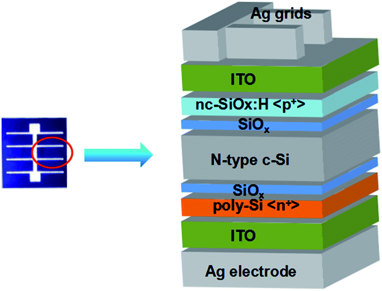 | ||
| Fig. 2 Photographic image (left) and schematic diagram (right) of TOPCon silicon solar cells with poly-Si passivated contact. | ||
The thicknesses of the layers were measured by the Bruker Dektak XT Stylus Profiler and the HORIBA Jobin-Yvon spectroscopic ellipsometry. The structural properties of the 100 nm layers were characterized by Raman spectroscopy (LabRAM-HR, 532 nm). To quantify the quality of the c-Si surface passivation, effective minority carrier lifetime (τeff) at a specific injection level of minority carrier density (MCD) of 1015 cm−3, the implied open-circuit voltage (iVoc) and saturation current density (J0) were measured by a Sinton Consulting WCT-120 lifetime tester using the transient mode. Here, iVoc and J0 at one sun is calculated according to the following equation:9,10
 | (1) |
 | (2) |
3. Results and discussion
The influence of the hydrogen dilution ratio on microstructure of the μc-Si:H films was analysed by Raman spectroscopy. The normalized Raman scattering spectra of the μc-Si:H films with different hydrogen dilution ratio R deposited on quartz substrates and the Gaussian fitting curve of Raman spectrum with R = 30 are presented in Fig. 3(a) and (b), respectively. As can be seen from Fig. 3(b), the Raman spectra of the μc-Si:H films can be fitted as the superposition of the scattering spectra of amorphous and microcrystalline silicon. Four Raman scattering spectra of amorphous silicon correspond to the vibrational modes as following: transverse acoustic (TA)-like mode at 150 cm−1, longitudinal acoustic (LA)-like mode at 310 cm−1, longitudinal optic (LO)-like mode at 400 cm−1 and transverse optic (TO)-like mode at 480 cm−1. At the same time, the scattering peaks at 510 cm−1 and 520 cm−1 correspond to the transverse optic (TO)-like vibrational mode of grain boundary and microcrystalline silicon.18–20 The results indicate that the μc-Si:H films are composed of amorphous and microcrystalline mixed phase structure. From Fig. 3(a), the intensity and peak position of Raman spectra changed with the different hydrogen dilution ratio which reveal the microstructural variation of μc-Si:H films. For the sample with the hydrogen dilution ratio R is 10, the Raman spectra corresponds to the amorphous vibrational modes completely, indicating that the sample is in amorphous structure. When the hydrogen dilution ratio R increases to 15, except for the prominent characteristic peaks for amorphous material, a small shoulder appears in the region of 510 cm−1, demonstrating that the formation of microcrystalline silicon phase in the film.18,21 By further increasing the hydrogen dilution ratio R, the peak intensity at 510 cm−1 has been enhanced, while the peak position could be observed blue shift to 520 cm−1 gradually. The results manifest that the microcrystalline composition in the films augment with increasing the hydrogen dilution ratio R.22 A quantitative analysis for crystallinity fraction (Xc) of the μc-Si:H films in all samples is calculated by the following formula: Xc = (Ic + Ii)/(Ic + Ii + Ia), where Ia, Ii and Ic denote the integrated area of the amorphous peak (480 cm−1), intermediate peak (510 cm−1) and crystalline peak (520 cm−1) in the Raman spectra respectively.23 Fig. 3(c) shows the calculated Xc values from Raman spectra fitting and the deposition rate as a function of hydrogen dilution ration R. It is observed that the Xc of the microcrystalline silicon films enhances gradually while the deposition rate shows a monotonous decline as the hydrogen dilution ratio R increases. When the hydrogen dilution ratio R is 15, the rising trend of the Xc curve starts to slow down, indicating that the microstructure of the μc-Si:H films is at the initial stage of amorphous-microcrystalline phase transition. | ||
| Fig. 3 (a) Raman spectra of μc-Si:H films with different hydrogen dilution ratio R. (b) Gaussian fitting curve of Raman spectrum with the R is 30. (c) Deposition rate and crystallinity fraction curve, (d) ITA/ITO curve of μc-Si:H films with different hydrogen dilution ratio R. | ||
To further characterize the structural properties of the μc-Si:H films with different hydrogen dilution ratio R, the ITA/ITO is defined for estimation the inter-medium-range structural order (IRO),20,24 where ITA and ITO are the integrated area of the amorphous silicon vibrational mode corresponding to the TA-like mode and TO-like mode in Raman spectra. The ITA/ITO curve with different hydrogen dilution ratio R is exhibited in Fig. 3(d). It clearly can be seen that the ITA/ITO values drop sharply by increasing the hydrogen dilution ratio R from 10 to 15, and the minimum value is reached at 15, which demonstrates that the microstructure of the films has been improved by higher middle-range ordered structure and hydrogen content.25–31 Thus, the defect density in the μc-Si:H films decreases. When increasing the hydrogen dilution ratio R from 15 to 30, the ITA/ITO curve first rises gradually, and then declines slowly at R is 30. This trend of ITA/ITO curve reveals that the μc-Si:H films evolves from amorphous to crystalline phase with increasing the hydrogen dilution ratio R. When the value of R is smaller, the microstructure of μc-Si:H film is dominant by amorphous phase with highly disordered structure. By increasing the R up to 15, the nucleation and growth of silicon micro-grain have been accelerated by even more active hydrogen atoms, and the microstructure of the μc-Si:H films is in the initial region of amorphous-microcrystalline phase transition.26 With further increasing the R from 15 to 25, voids of the film could be formed due to the etching effect of weaker bonds by active hydrogen atoms, the overall order of the microstructure in the films begins to decline while the crystallinity of the films is enhanced.27 Under the condition of higher hydrogen dilution, the hydrogen atoms will release a certain amount of energy while saturate the silicon dangling bonds on the surface of the silicon film. This two effects increase the diffusion length of the reaction precursor, especially SiH3, on growth surface of the film, thereby promote the nucleation and growth of grains. During the growth of grains, grain boundaries and micro-voids will be formed, and there are mainly SiH2 bonds on the surface.28 However, when the value of R is 30, the grains in the film become larger while the active hydrogen passivates the defects and holes between the grain boundary at the same time, so the quality of the film seems to get better again.29
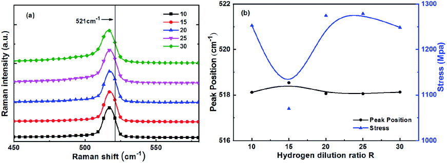
Fig. 4(a) shows the Raman spectra of the poly-Si films after annealing. All μc-Si:H films deposited on quartz substrate were annealed in nitrogen atmosphere at 800 °C for 30 minutes. The spectra curves indicate that the amorphous phase disappears through post-deposition annealing treatment, and the consistent sharp peak around 520 cm−1 related to the crystalline phase could be seen. The results demonstrate that the crystallization of the μc-Si:H samples was significantly enhanced after thermal treatment, thus the high crystallization poly-Si films were prepared. This is mainly attributed to the decrease of Si–H bonds corresponding to the reduction of the amorphous matrix, while an increase of covalent Si–Si bonds promoting the increased crystallinity and a significant reduction of the density of SiHx bonds in the films through annealing. Moreover, the high temperature post-deposition treatment may lead to a tendency for structural improvement of the short range order in the grown layer and a decrease of the disorder in the film network. Therefore, the equilibrium in the c-Si substrate interface and the bulk of the poly-Si film can occur, involving short-range H diffusion and local network redistribution.23 It is generally known that the density of crystalline silicon is about 3% higher than amorphous silicon, so the defects in the interior and interface of the films could be generated to mitigate the stress due to the crystallinity of the Si films.31,32 In order to estimate the internal stress of poly-Si film, the Raman scattering spectrum of annealed samples was Gaussian fitted. The peak position deviation between the TO-like vibrational mode of the poly-Si and monocrystalline silicon (521 cm−1) is proportionate to the stress in the Si films (Δω = 1 cm−1 corresponds about 435 MPa).33,34 Fig. 4(b) presents the peak position of TO-like vibrational mode and internal stress curve of poly-Si films formed through high temperature post-deposition annealing with different hydrogen dilution ratio R. It can be seen that the minimum variance of Raman spectra peak position is obtained when hydrogen dilution ratio R is 15, the corresponding stress distribution is lower which demonstrated lower defects in the Si films.
 | ||
| Fig. 4 (a) Raman scattering spectra, (b) the peak position of TO-like vibrational mode and internal stress curve of poly-Si films formed through high temperature post-deposition annealing with different hydrogen dilution ratio R. | ||
The passivation effect with the microstructure and film quality of the poly-Si film was studied by effective minority carrier lifetime. Fig. 5(a) shows the effective minority carrier lifetime (τeff) and Fig. 5(b) presents the iVoc and J0 variation curve of symmetrical structure of the poly-Si passivated contact with different hydrogen dilution ratio R. The inset in Fig. 5(a) illustrates the τeff at a specific injection level of MCD of 1015 cm−3. As can be seen, the τeff is improved when increasing hydrogen dilution ratio R, reaches its peak at R = 15 and is reduced at higher hydrogen dilution. The iVoc exhibits a similar tendency to τeff from Fig. 5(b), while the change trend of the J0 is opposite. With the increase of hydrogen dilution ratio R from 10 to 15, the τeff for the samples improve significantly, especially at low injection level. The maximum value of τeff reaches 1.75 ms, and the iVoc dramatically increases to 690 mv while the corresponding J0 drops to 45 fA cm−2. The results suggest that increasing hydrogen dilution rate helped to improve the passivation quality.11,12 This can be explained by the microstructure evolution during the deposition of the μc-Si:H films with different hydrogen dilution ratio R. When R is 15, phase transition from amorphous phase to microcrystalline phase occurs in μc-Si:H film, the hydrogen atom content is higher and the structure becomes more ordered as mentioned above from Fig. 3. It should be noted that, the hydrogen effusion which is provided from the breaking of weakly bonded hydrogen coming from SiH2-bonding and SiH3-bonding, as well as strongly bonded hydrogen of isolated Si–H bonds could be appeared during the recrystallization of μc-Si:H film.1,17 A mass of atomic hydrogen diffused from Si film to c-Si surface can reduce the interface defect density, thus the chemical passivation quality is improved and the entire injection level dependent τeff is significantly increased.20 Moreover, the higher bulk quality of poly-Si film due to ordered structure and decreased defect density will enhance the carrier transportation, thus the field effect passivation takes effect and the τeff at low injection level is raised.13,20
 | ||
| Fig. 5 (a) The effective minority carrier lifetime (τeff), the inset illustrates the τeff at a specific injection level of MCD of 1015 cm−3, (b) iVoc and J0 variation curve of the symmetrical structure of the poly-Si passivated contact with different hydrogen dilution ratio R. | ||
Consequently, the efficient passivation on the c-Si surface can be ascribed to the simultaneously enhanced field effect passivation and defect passivation from poly-Si film. As further increase the hydrogen dilution ratio R, the hydrogen content in the Si films is decreased with higher crystallinity, so the defect states on the crystalline silicon surface can be not effectively passivated, the τeff and iVoc show a downward trend while the saturated current density J0 increases rapidly.
To reveal the influence of interface passivation on photovoltaic performances of TOPCon silicon solar cells with poly-Si passivated contact, illuminated J–V response of devices containing poly-Si film with different hydrogen dilution were analysed. TOPCon silicon solar cells were fabricated according to the device structure in Fig. 2. Fig. 6(a) exhibits the illuminated J–V curves of TOPCon silicon solar cells containing poly-Si film with different hydrogen dilution ratio R, and the corresponding electrical parameters are shown in Fig. 6(b)–(d). It can be found that the photovoltaic properties of the fabricated devices firstly improve and then degrade with the increasing hydrogen dilution in poly-Si layer. As presented in Fig. 6(b)–(d), all the electrical parameters show similar variation trend. The critical factors in high-efficiency TOPCon silicon solar cells are the passivation quality at c-Si interface and the film quality of poly-Si layer.35 The efficient passivation would reduce the defect density near c-Si surface and then suppress the defect-induced recombination velocity. In addition, the improved quality of the poly-Si film can also accelerate the carrier transportation. In case of hydrogen dilution ratio R is 10, the devices Voc, Jsc and FF are 624 mV, 35.18 mA cm−2 and 76.43%, respectively, with a conversion efficiency of 16.79%. Coupled with the effect of serious interface defects and lower built-in potential caused by lattice difference between Si layer and c-Si interface and less phosphorus doping in amorphous silicon film, the corresponding devices performance appears poor. As the R increases to 15, the cells performance is obviously enhanced and the best result is achieved, the devices Voc, Jsc and FF are 638 mV, 36.16 mA cm−2 and 77.6%, possessing a CE up to 17.91%. It is worth mentioning that the front surface of the device is not optimized for texturing and interface passivation, so this efficiency is relatively excellent.17
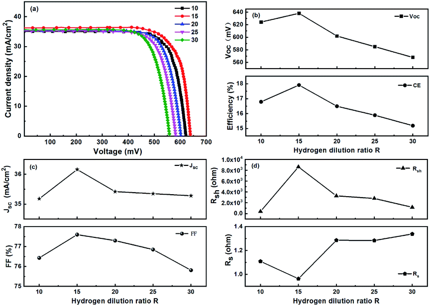 | ||
| Fig. 6 (a) Light J–V characterization of the TOPCon silicon solar cell with different hydrogen dilution ratio R. (b–d) Photovoltaic characteristics from the light J–V of devices under the standard one-sun conditions. | ||
This result can be attributed to the reduction of carrier recombination velocity near the passivated c-Si surface and the decreased bulk defect density in poly-Si layer. It should be mentioned that the improvement of Voc can be ascribed to the reduced recombination loss owing to the decreasing defect density by hydrogen diffusion. In terms of the improved Jsc and FF, it is mainly attributed to the efficient carrier separation and extraction caused by high quality of poly-Si film. This also can be demonstrated by higher Rsh and lower Rs from Fig. 6(d), which indicates lower leakage current and higher conductivity, respectively. When the hydrogen dilution ratio R increases further, the electrical properties turn to decrease which is caused by the aggravated defect recombination and deteriorated carrier transportation, due to the degraded interface passivation and poly-Si quality.
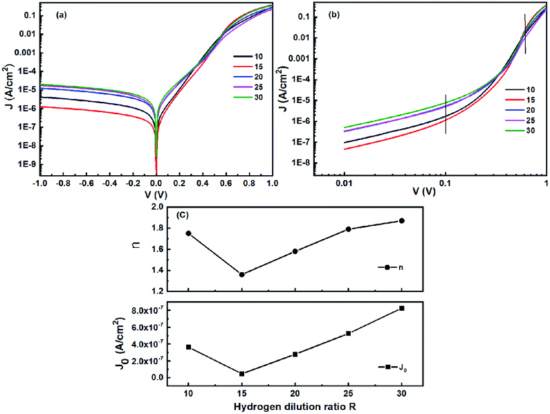
Fig. 7 presents the dark J–V characteristic of TOPCon solar cells to clarify the carrier transport mechanism in the devices. From the semi-logarithmic J–V curves in Fig. 7(a), all of the devices exhibited obvious rectifying behavior. As can be seen, the increasing hydrogen dilution in poly-Si film improves the rectifying ratio and the maximum value 3 × 10⁵ is obtained at R of 15, indicating the excellent diode formed in the devices, the result mainly attributes to the reduced defect density at the c-Si interface and enhanced field effect passivation from high quality poly-Si film. Fig. 7(b) shows the double-logarithmic plot of the dark J–V curves in the forward voltage rang. It can be found that there are three obviously linear regions with different J–V-slopes in the dark J–V curves, indicating the different dominating carrier transport mechanism from 0 to 1 V. At low voltages (V < 0.1 V), the dark current density is mainly determined by the shunt resistance. At intermediate voltages (V ∼ 0.1–0.6 V), the electrical transporting mechanism is dominated by the diffusion-limited model or the recombination-limited model. In higher voltages (V > 0.6 V), the series resistance mainly influences the carrier transport in this range. The ideality factor (n) and the reverse saturation current density (J0) of the devices were extracted by fitting the dark J–V curve at the intermediate voltage with the diode equation: J = J0[exp(qV/nKT) − 1],36 Where k is the Boltzmann constant, q is the electronic charge and T is the temperature. As the fitting results shown in Fig. 7(c), the ideality factor of the devices is 1.75 and the corresponding J0 is 3.63 × 10⁻⁷ A cm−2 when R is 10, indicating that the dominated carrier transport mechanism is the recombination transportation near the c-Si interface. With increasing the hydrogen dilution ratio R to 15, the n and J0 parameters obtain the minimum value of 1.36 and 4.62 × 10⁻⁸ A cm−2, indicating that the dominated carrier transport mechanism is the diffusion transportation and the recombination current has been suppressed. This results could mainly ascribed to the lower carrier recombination loss and the higher built-in potential owing to the less defects density at the c-Si interface and the high quality of the poly-Si film. As the hydrogen dilution ratio R increases further, the n and J0 gradually rise either, implying that the notable impact of carrier recombination near the c-Si interface on the dark current. This is mainly due to the increased defects density at the c-Si interface and the Si films. Correspondingly, the carrier transportion of the devices is limited and the recombination current increases.
 | ||
| Fig. 7 (a) The semi-logarithmic plot of the dark J–V curves for the TOPCon solar cells with poly-Si passivated contact at different hydrogen dilution ratio R. (b) The double-logarithmic plot of the dark J–V curves for devices in the forward voltage range. (c) The n and J0 parameters of the devices fitted from the double-logarithmic plot of the dark J–V curves. | ||
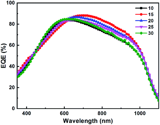
The photo-response characteristics of fabricated TOPCon silicon solar cells with different hydrogen dilution ratio were analyzed by external quantum efficiency spectra, which was illustrated in Fig. 8. It can be seen that the EQE of TOPCon solar cells first increases notably and then falls gradually by increasing the hydrogen dilution ratio R. It is known that the carrier transport at the c-Si interface is the limiting factor for photo-response of the devices in the long wavelength range. When R is 10, the EQE appears poor due to the disordered microstructure of the Si film. By increasing the hydrogen dilution ratio R from 10 to 15, the EQE improves significantly in the long wavelength range from 600–1100 nm. As illustrated in Fig. 3, along with the microstructure transition of the Si layer, the ordered microstructure and improved doping level leading to reduce defects density and enhance carrier transportation at c-Si interface, so the highest EQE value is obtained when R is 15. However, when the hydrogen dilution ratio R increases further, the EQE shows a gradually decline trend in the long wavelength and when going to 30, the EQE is even equivalent to the device with R is 10, which is consist with the electric parameter presented from Fig. 6. This observation mainly attributes to the increasing stress results the higher bulk defects and carrier recombination probability in Si layer. Besides, the serious defects recombination at c-Si interface lead to the reduction of Voc and shunt resistance, which hinder the majority carrier transportation at silicon surface. The two effects contribute together to the declined EQE of devices for higher hydrogen dilution. Based on the above analysis, the moderate hydrogen dilution process plays a crucial role in obtaining an enhanced photo-response in TOPCon silicon solar cells.
 | ||
| Fig. 8 External quantum efficiency of TOPCon silicon solar cells with different hydrogen dilution ratio R. | ||
4. Conclusions
In this study, we verified a effective method of hydrogen dilution to improve the interface passivation on the c-Si surface and enhance the photovoltaic properties of TOPCon solar cells. The poly-Si layers were recrystallized from phosphorus-doped μc-Si:H layers pre-deposited using PECVD method by high temperature post-deposition annealing. The results demonstrated that, with increasing the hydrogen dilution ratio R, the microstructure of μc-Si:H layers transformed from amorphous phase to microcrystalline phase. The improved quality could ascribe to the ordered microstructure and higher hydrogen content of Si layer at the initial region of phase transition. Meanwhile, the effective minority carrier lifetime of symmetrical structure with poly-Si passivated contact attained a maximum of 1.75 ms, owing to the improved field effect passivation by poly-Si film and reduced defects density at c-Si surface by appropriate hydrogen diffusion during the thermal treatment. As a consequence, the TOPCon solar cells conversion efficiency is significantly enhanced and the maximum value of 17.91% is achieved at R = 15. The optimalized rectifying ratio of the fabricated devices is up to 3 × 10⁵, implying that the carrier transport mechanism at c-Si interface dominates by the diffusion-limited mechanism with the recombination current effectively suppressed. Correspondingly, the photo response of cells remarkably enhances in the long wavelength range, which is due to the decreasing defect recombination and the improved carrier transport at c-Si surface. The present work optimized the quality of Si film by adjusting the hydrogen dilution, which provided a simple and effective process method for improving the photoelectric conversion efficiency of TOPCon silicon solar cells.Conflicts of interest
There are no conflicts to declare.Acknowledgements
This study was supported financially by the National Key Research and Development Program of China (Grant No. 2018YFB1500503-02); the Natural Science Foundation of Hebei Province, P. R. China (Grant No. E2021201014 and F2018201058) and Foundation of President of Hebei University, P. R. China (Grant No. XZJJ201903).References
- S. B. Amor, H. Meddeb, R. Daik, A. B. Othman, S. B. Slama, W. Dimassi and H. Ezzaouia, Appl. Surf. Sci., 2016, 360, 572–578 CrossRef CAS.
- Y. Xu, H. Shen, Z. Yang, Q. Wei, Z. Ni, S. bing, Z. Wang and B. Zhao, Sol. Energy, 2020, 207, 436–440 CrossRef CAS.
- J. Zhao, A. Wang and M. A. Green, Prog. Photovoltaics, 1999, 7, 471–474 CAS.
- M. A. Green, Prog. Photovoltaics, 2009, 17, 183–189 CAS.
- J. Chen, D. Daniel, K. Ge, H. Li and B. S. Flavel, Adv. Funct. Mater., 2020, 30, 2000484 CrossRef CAS.
- A. Richter, J. Benick, F. Feldmann, A. Fell, M. Hermle and S. W. Glunz, Sol. Energy Mater. Sol. Cells, 2017, 173, 96–105 CrossRef CAS.
- F. Feldmann, M. Bivour, C. Reichel, H. Steinkemper, M. Hermle and S. W. Glunz, Sol. Energy Mater. Sol. Cells, 2014, 131, 46–50 CrossRef CAS.
- Y. Tao, K. Madani, E. Cho, B. Rounsaville, V. Upadhyaya and A. Rohatgi, Appl. Phys. Lett., 2017, 110, 021101 CrossRef.
- F. Feldmann, M. Bivour, C. Reichel, R. Christian, H. Martin and S. W. Glunz, Sol. Energy Mater. Sol. Cells, 2014, 120, 270–274 CrossRef CAS.
- Y. Tao, E. L. Chang, A. Upadhyaya, B. Roundaville, Y. W. Ok, K. Madani, C. W. Chen, K. Tate, V. Upadhyaya, F. Zimbardi, J. Keane, A. M. Payne and A. Rohatgi, 2015 IEEE 42nd PVSC, 2015, pp. 1–5 Search PubMed.
- T. N. Truong, D. Yan, C. Samundsett, R. Basnet, M. Tebyetekerwa, L. Li, F. Kremer, A. Cuevas, D. Macdonald and H. T. Nguyen, ACS Appl. Mater. Interfaces, 2019, 11, 5554–5560 CrossRef CAS PubMed.
- J. I. Polzin, B. Hammann, T. Niewelt, W. Kwapil, M. Hermle and F. Feldmann, Sol. Energy Mater. Sol. Cells, 2021, 230, 111267 CrossRef CAS.
- C. Hollemann, N. Folchert, S. P. Harvey, P. Stradins, D. L. Young, C. L. Souza, M. Rienäcker, F. Haase, R. Brendel and R. Peibst, Sol. Energy Mater. Sol. Cells, 2021, 231, 111297 CrossRef CAS.
- Z. Rui, Y. Zeng, X. Guo, Q. Yang, Z. Wang, C. Shou, W. Ding, J. Yang, X. Zhang, Q. Wang, H. Jin, M. Liao, S. Huang, B. Yan and J. Ye, Sol. Energy, 2019, 194, 18–26 CrossRef CAS.
- F. Feldmann, M. Simon, M. Bivour, C. Reichel, M. Hermle and S. W. Glunz, Appl. Phys. Lett., 2014, 104, 181105 CrossRef.
- Q. Li, K. Tao, Y. Sun, R. Jia, S. Wang, Z. Jin and X. Liu, Sol. Energy, 2016, 135, 487–492 CrossRef CAS.
- K. Tao, Q. Li, C. Hou, S. Jiang, J. Wang, R. Jia, Y. Sun, Y. Li, Z. Jin and X. Liu, Sol. Energy, 2017, 144, 735–739 CrossRef CAS.
- A. T. Voutsas, M. K. Hatalis, J. Boyce and A. Chiang, J. Appl. Phys., 1995, 78, 6999–7006 CrossRef CAS.
- N. Maley and J. S. Lannin, Phys. Rev. B: Condens. Matter Mater. Phys., 1987, 36, 1146 CrossRef CAS PubMed.
- Y. Zhang, R. Cong, W. Zhao, Y. Li, C. Jin, W. Yu and G. Fu, Sci. Bull., 2016, 61, 787–793 CrossRef CAS.
- L. Houben, M. Luysberg, P. Hapke, R. Carius, F. Finger and H. Wagner, Philos. Mag. A, 1998, 77, 1447–1460 CAS.
- T. Kamiya, K. Nakahata, Y. T. Tan, Z. A. K. Durrani and I. Shimizu, J. Appl. Phys., 2001, 89, 6265–6271 CrossRef CAS.
- S. B. Amor, R. Bousbih, R. Ouertani, W. Dimassi and H. Ezzaouia, Sol. Energy, 2014, 103, 12–18 CrossRef.
- R. L. C. Vink, G. T. Barkema and D. W. W. F. Van, Phys. Rev. B: Condens. Matter Mater. Phys., 2001, 63, 115210 CrossRef.
- P. R. Poulsen, M. Wang, J. Xu, W. Li, K. Chen, G. Wang and D. Feng, J. Appl. Phys., 1998, 84, 3386–3391 CrossRef CAS.
- J. Geissbühler, S. D. Wolf, B. Demaurex, J. P. Seif, D. T. L. Alexander, L. Barraud and C. Ballif, Appl. Phys. Lett., 2013, 102, 231604 CrossRef.
- A. Matsuda, Thin Solid Films, 1999, 337, 1–6 CrossRef CAS.
- G. van Elzakker, V. Nádaždy, F. D. Tichelaar, J. W. Metselaar and M. Zeman, Thin Solid Films, 2006, 511–512, 252–257 CrossRef CAS.
- W. Zhao, L. Du, Z. Jiang, C. Chen, W. Yu and G. Fu, Chin. Phys. B, 2015, 24, 108102 CrossRef.
- S. Miyazaki, N. Fukuhara and M. Hirose, J. Non-Cryst. Solids, 2000, 266, 59–63 CrossRef.
- M. D. Efremov, V. V. Bolotov, V. A. Volodin, L. I. Fedina and E. A. Lipatnikov, J. Phys.: Condens. Matter, 1996, 8, 273 CrossRef CAS.
- A. Wellner, V. Paillard, C. Bonafos and H. Coffin, J. Appl. Phys., 2003, 94, 5639–5642 CrossRef CAS.
- Y. Lin, Z. Yang, Z. Liu, J. Zheng, M. Feng, Y. Zhi, L. Lu, M. Liao, W. Liu and D. Ma, Energy Environ. Sci., 2021, 14, 6406–6418 RSC.
- Y. Kang, Q. Yu, Z. Lei and H. Ming, Opt Laser. Eng., 2005, 43, 847–855 CrossRef.
- L. Tutsch, F. Feldmann, B. Macco, M. Bivour, E. Kessels and M. Hermle, IEEE J. Photovoltaics, 2020, 10, 986–991 Search PubMed.
- D. Song, E. C. Cho, G. Conibeer, Y. Huang and M. A. Green, Appl. Phys. Lett., 2007, 91, 123510 CrossRef.
| This journal is © The Royal Society of Chemistry 2022 |