
 Open Access Article
 This Open Access Article is licensed under a Creative Commons Attribution-Non Commercial 3.0 Unported Licence
Study on SO2 and Cl2 sensor application of 2D PbSe based on first principles calculations
Jiwei Zhang a,
Jianhua Pang*a,
Hui Chena,
Guang Weia,
Songrui Wei*b,
Jin Yana and
Shaowei Jinc
a,
Jianhua Pang*a,
Hui Chena,
Guang Weia,
Songrui Wei*b,
Jin Yana and
Shaowei Jinc
aGuangdong Ocean University, Zhanjiang 524088, China. E-mail: njpjh@sina.com
bInstitute of Microscale Optoelectronics, Shenzhen University, Shenzhen 518060, China. E-mail: weisongrui@126.com
cNational Supercomputing Center in Shenzhen (Shenzhen Cloud Computing Center), Shenzhen 518055, China
First published on 17th March 2022
Abstract
In this paper, we use 2D PbSe to design a gas sensor to monitor the presence of SO2 and Cl2. We use first principles to verify the feasibility of this material, such as atomic structure, band gap, differential charge density and Bader charge. The results show that 2D PbSe can distinctly adsorb SO2 and Cl2. Furthermore, the adsorption of SO2 and Cl2 will affect the electronic structure of 2D PbSe, and some electrons in the PbSe are transferred to gas atoms. The band gap of the system after adsorption is smaller than that of the PbSe before adsorption. The band gap of single layer PbSe decreases by 41.92% after SO2 adsorption and 60.61% after Cl2 adsorption. The band gap of multi-layer PbSe decreases by 72.97% after SO2 adsorption and 43.24% after Cl2 adsorption. This shows that single layer PbSe is more sensitive to Cl2 and multi-layer PbSe is more sensitive to SO2. It provides a potential possibility for designing gas sensors for SO2 and Cl2 based on 2D PbSe.
1. Introduction
Two-dimensional materials are considered as excellent new materials due to their good conductivity, damage resistance, heat shock resistance, ease of processing and other advantages.1 Many 2D materials show outstanding performance in various fields because of their unique properties, such as enhanced optical transparency, excellent conductivity and outstanding mechanical strength.2–5 More than 30 MXene materials are synthesized experimentally, and hundreds of possible compositions are predicted theoretically.6 Among them, some MXene materials are more suitable as gas sensor materials because of their adjustable band gap.7–9Cl2 is a highly toxic gas with a strong pungent odour, and it can cause great damage to the human respiratory system.10 SO2 is a kind of irritant sulfur oxide, one of the main pollutants in the atmosphere, and the major contributor to acid rain. At the same time, it is a kind of carcinogen, and long-term exposure to industrial pollutants containing high levels of SO2 can increase the risk of cancer.11 In this context, the effective detection of these harmful gases is useful to protect the environment and human health.12,13
PbSe is a binary lead sulfur compound, and this material has performed well in the fields of photoelectric detection, photoluminescence and so on.14,15 According to the reference, PbSe with rocksalt structures can be prepared as monolayer PbSe by mechanical exfoliation and wet chemical synthesis.16–21 In this way, its surface area will be greatly increased and it will become more sensitive. At the same time, we find that Wang's report showed that Cl doping caused the decrease of PbSe resistance.22 Therefore, it is feasible to detect Cl2 with PbSe.
In this paper, based on first principle calculation, we study the adsorption property of the single layer PbSe material and multi-layer PbSe. We find that the 2D PbSe can adsorb SO2 and Cl2. When Cl2 is adsorbed on PbSe, the bond between Cl atoms breaks. However, for SO2, the bond does not break. Additionally, we also find electron transfer in the adsorption process. It helps to understand the physical origin of the adsorption process and change of conduction. Based on the change of conduction, we can judge whether the material adsorbs Cl2 and SO2. Based on these results, the PbSe is a potential sensor material for monitoring the presence of SO2 and Cl2 in the environment.
2. Materials and methods
All calculations are carried out using the density functional theory, implemented in Vienna Ab Initio Simulation Package (VASP).23–25 Due to the large computing system, the exchange–correlation potential is employed by the generalized gradient approximation (GGA) with Perdew–Burke–Ernzerhof (PBE) functional.26,27 The GGA take uneven distribution of the electron into account, making the results of the calculated values are more accurate.28 In order to better understand van der Waals, the DFT-D3 method in Grimme is applied to the calculation.29 At the same time, we also carry out adsorption energy correction about zero point vibrational energy. In order to evaluate the adsorption capacity of PbSe nanoplates to SO2 and Cl2, we use a single layer PbSe with a vacuum layer thickness of 30 Å and a multi-layer PbSe structure with a vacuum layer thickness of 40 Å. During structure optimization and electronic self-consistent calculation, a plane wave cut-off of 500 eV and a k-point mesh of 3 × 3 × 1 in the Gamma sampling scheme are used. The EDIFFG of structure optimization is 10−5 eV, and the EDIFFG of electronic self-consistent is 10−7 eV. Also, we select three high symmetry points: Γ, M and K, and twenty k points are taken between every two highly symmetrical points in the band calculation. The cut-off energy of 500 eV is also adopted throughout the band calculation, until the threshold of 10−7 eV is reached. The single layer and multi-layer structures of 2D PbSe are shown in Fig. 1. The single layer PbSe has a rocksalt crystal structure, and Delerue C. has reported the synthesis and microstructure of this material.21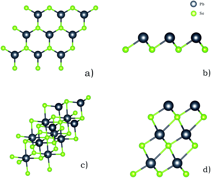 | ||
| Fig. 1 Single layer PbSe and multi-layer PbSe structure ((a) is single layer PbSe, and (b) is a side view of it; (c) is multi-layer PbSe, and (d) is a side view of it). | ||
The adsorption energy is obtained from the following formula:
| E = Etotal − EPbSe − Egas | (1) |
3. Results and discussion
First of all, we calculate the adsorption energy of SO2 and Cl2 on single layer PbSe. The results are shown in Table 1. In this table, PbSeSO2 is the adsorption system of SO2 and single layer PbSe. PbSeCl2 is the adsorption system of Cl2 and single layer PbSe. It is found that the adsorption energy of SO2 and Cl2 are both negative. So, SO2 and Cl2 molecular can be easily adsorbed on single layer PbSe. It is the basis for sensor applications.| Material | Cl2 | PbSe | PbSeCl2 | Adsorption energy |
|---|---|---|---|---|
| Energy (eV) | −3.73 | −72.95 | −79.38 | −2.70 |
| Material | SO2 | PbSe | PbSeSO2 | Adsorption energy |
|---|---|---|---|---|
| Energy (eV) | −17.22 | −72.95 | −90.50 | −0.33 |
At the same time, we also consider the effect of van der Waals (vdW) on the adsorption energy. The results are shown in Table 2. According to the analysis, we can find that without considering the influence of vdW, the adsorption energy of single layer PbSe for both gases is positive. On the contrary, after considering the influence of vdW, the adsorption energy of single layer PbSe for both gases is negative. Therefore, the vdW plays an important role in the adsorption of single layer PbSe to Cl2 and SO2.
| Material | Cl2 | PbSe | PbSeCl2 | Adsorption energy |
|---|---|---|---|---|
| Energy (eV) | −3.73 | −72.95 | −76.10 | 0.58 |
| Material | SO2 | PbSe | PbSeSO2 | Adsorption energy |
|---|---|---|---|---|
| Energy (eV) | −17.22 | −72.95 | −86.56 | 3.61 |
We find that the bond length of Cl–Cl changed greatly, the bond length before adsorption is 1.99 Å, the bond length after adsorption is 6.14 Å. So, we can draw a conclusion that chemisorption occurs simultaneously when PbSe adsorbs Cl2. The larger adsorption energy in Table 1 also proves this situation. However, we didn't find this situation before and after PbSe adsorbs SO2.
As for adsorption sites, we explore the adsorption of gas on both sides of 2D materials. It is found that the Se atom side cannot adsorb SO2 and Cl2 while the Pb atom side can adsorb SO2 and Cl2.
Traditional, conductivity is usually used as indicator of many sensors. If the change of conductivity is larger before and after the adsorption, the sensor is more sensitive. As the conductivity is related with the size of band gap, we calculate the band gap before and after the adsorption. The results of single layer PbSe are shown in Fig. 2. The band gap of PbSe, PbSeCl2 and PbSeSO2 are 1.98 eV, 0.78 eV and 1.15 eV, respectively. From these data, we can find that with the adsorption of SO2 and Cl2, the band gap of the material decreases obviously, it means that the conductivity of the material is significantly enhanced,31–33 the smaller band gap after Cl2 is adsorbed corresponds to the smaller PbSe resistance caused by Cl doping in Wang's report. So, conductivity is a sensitive indicator for detecting SO2 and Cl2 for single layer PbSe.
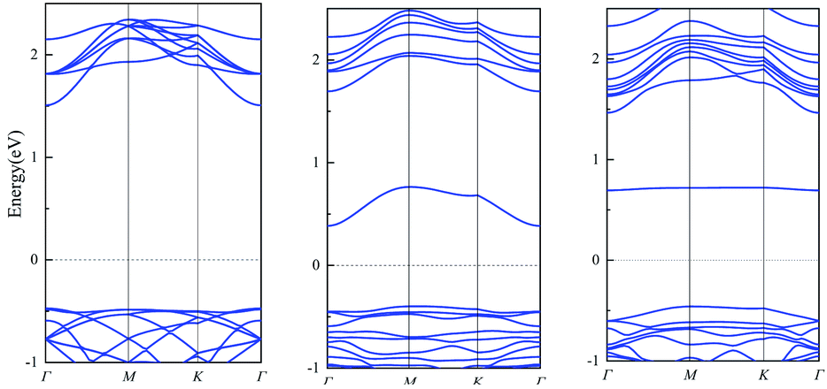 | ||
| Fig. 2 The band diagram before and after adsorption ((left) shows the energy band diagram of single layer PbSe, (mid) shows the energy band diagram of PbSeCl2 adsorption system, and (right) shows the energy band diagram of PbSeSO2 adsorption system). | ||
The selection specificity of sensors is also investigated. In order to ensure that the sensor is not affected by other gases in the air, we calculate the adsorption of N2 and O2, they account for the largest proportion in the air. The adsorption energies of N2 and O2 are positive. So, N2 and O2 cannot adsorb on 2D PbSe and it will not cause significant changes in conductivity due to the presence of O2 and N2 in the air.
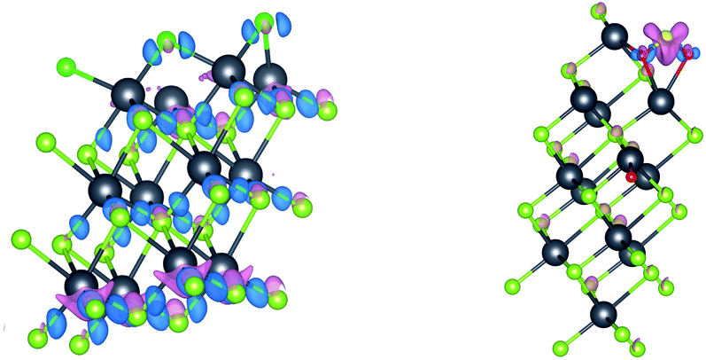
In order to further explore the adsorption of SO2 and Cl2 on PbSe, we study the electron transfer. We calculate the differential charge density and the Bader charge.34,35 The details are shown in Table 3 and Fig. 3. For Fig. 3, the blue part is the electron loss area and the purple part is the electron gain area. We can see that the Cl–Cl bond between Cl atoms breaks after the Cl2 is absorbed by PbSe, while the chemical bond in SO2 of S atom and O atom in Bader charge calculation. We can conclude that the adsorption of monolayer PbSe to Cl2 is chemical adsorption, and the adsorption of monolayer PbSe to SO2 is physical adsorption.
| Atom | Before adsorption (e) | After adsorption (e) | Gain (+) and loss (−) electron (e) |
|---|---|---|---|
| Cl | 6.994 | 7.665 | +0.671 |
| Cl | 6.995 | 7.591 | +0.596 |
| S | 3.694 | 4.000 | +0.306 |
| O | 7.144 | 7.205 | +0.061 |
| O | 7.144 | 7.203 | +0.059 |
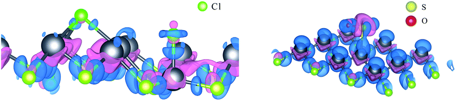 | ||
| Fig. 3 Differential charge density diagram after single layer PbSe adsorption ((left) shows PbSeCl2 adsorption system and (right) shows PbSeSO2 adsorption system). | ||
From the differential charge density diagram, it is found that the charge density of Pb atoms near the adsorption gas changes significantly, and the electrons have been transferred from the Pb atoms, resulting in changes in the electron densities around Cl and S atoms. Therefore, we can conclude that the interaction between the single layer PbSe and the adsorption gas changes the electronic structure of both the 2D material and gas molecular and the electronic transport property of the single layer PbSe.
For Table 3, we can see that all gas atoms get electrons. Among them, Cl atoms get the most electrons, while O atoms get almost no electrons, but the S atom get some electrons. So, the S atom must have got some electrons from PbSe. Fig. 3 proves this, the Pb atom near the S atom transfers some electrons to the S atom.
Meanwhile, we also explore the multi-layer PbSe (muPbSe). It consists three single layers of PbSe. The adsorption energies of SO2 and Cl2 on muPbSe are calculated. The results are shown in Table 4, where muPbSeSO2 is the adsorption system of SO2 and multi-layer PbSe, and muPbSeCl2 is the adsorption system of Cl2 and multi-layer PbSe. It is found that SO2 and Cl2 can also be adsorbed on muPbSe.
| Material | Cl2 | muPbSe | muPbSeCl2 | Adsorption energy |
|---|---|---|---|---|
| Energy (eV) | −3.73 | −100.76 | −108.57 | −4.08 |
| Material | SO2 | muPbSe | muPbSeSO2 | Adsorption energy |
|---|---|---|---|---|
| Energy (eV) | −17.22 | −100.76 | −119.02 | −1.03 |
At the same time, we also consider the effect of vdW on the adsorption energy. The results are shown in Table 5. According to the analysis, we can find that without considering the influence of vdW, the adsorption energy of multi-layer PbSe for both gases is positive. On the contrary, after considering the influence of vdW, the adsorption energy of multi-layer PbSe for both gases is negative. Therefore, the vdW plays an important role in the adsorption of multi-layer PbSe to Cl2 and SO2.
| Material | Cl2 | muPbSe | muPbSeCl2 | Adsorption energy |
|---|---|---|---|---|
| Energy (eV) | −3.73 | −100.76 | −101.31 | 3.18 |
| Material | SO2 | muPbSe | muPbSeSO2 | Adsorption energy |
|---|---|---|---|---|
| Energy (eV) | −17.22 | −100.76 | −111.74 | 6.24 |
We also find that the bond length of Cl–Cl changed greatly, the bond length after adsorption is 4.25 Å. So, we can draw a conclusion that chemisorption occurs simultaneously when muPbSe adsorbs Cl2. The larger adsorption energy in Table 4 also proves this situation. However, we didn't find this situation before and after muPbSe adsorbs SO2. Because of the chemisorption, Cl atoms are difficult to desorb from materials, PbSe can only be used as disposable gas detection material when used to detect Cl2.
The band structures of muPbSe, muPbSeSO2 and muPbSeCl2 are shown in Fig. 4. The band gap of muPbSe, muPbSeCl2 and muPbSeSO2 are 0.74 eV, 0.42 eV and 0.20 eV, respectively. The band gap decreases when PbSe changes from single layer to three layers, which is consistent with Li's research.36 Thus, multi-layer PbSe can still be used as gas sensor for Cl2 and SO2. At the same time, by analyzing the changes in the band gap between multi-layer PbSe and single layer PbSe before and after adsorption, it can be found that the band gap of multi-layer PbSe decrease by 72.97% before and after SO2 adsorption, the band gap of multi-layer PbSe decrease by 43.24% before and after Cl2 adsorption. The band gap of single layer PbSe decrease by 41.92% before and after SO2 adsorption, the band gap of single layer PbSe decrease by 60.61% before and after Cl2 adsorption. So, we can draw a conclusion that single layer PbSe is more sensitive to Cl2 and multi-layer PbSe is more sensitive to SO2.
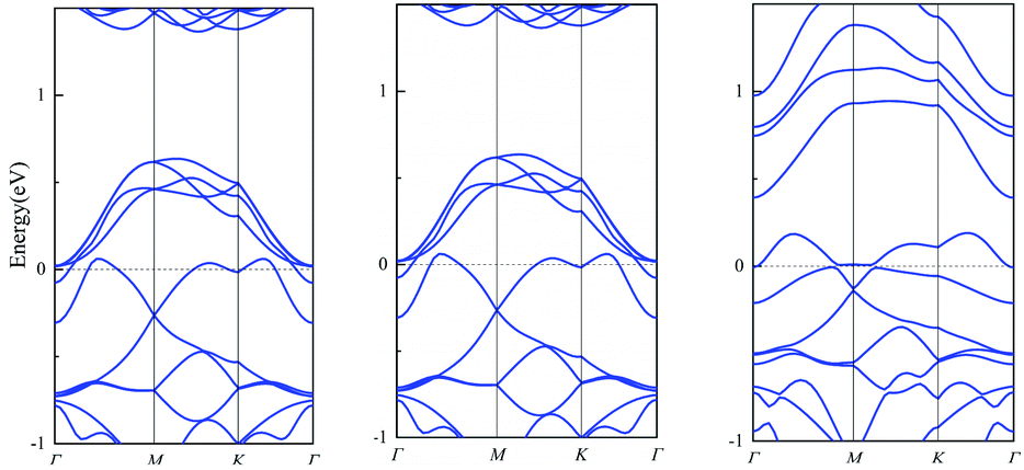 | ||
| Fig. 4 The band diagram before and after adsorption ((left) shows the band diagram of muPbSe, (mid) shows the band diagram of muPbSeCl2 adsorption system, and (right) shows the band diagram of muPbSeSO2 adsorption system). | ||
The Bader charge of muPbSe is shown in Table 6. It can be seen that there is charge transfer between the gas and the 2D material. The situation is similar to that of single-layer PbSe adsorption SO2 and Cl2. Cl atoms still get more electrons, and we can compare the situation with adsorption energy, larger adsorption energy corresponds to more electron transfer. And Pb atoms near adsorbed gas molecules still provide the most electrons.
| Atom | Before adsorption (e) | After adsorption (e) | Gain (+) and loss (−) electron (e) |
|---|---|---|---|
| Cl | 6.994 | 7.628 | +0.634 |
| Cl | 6.995 | 7.623 | +0.628 |
| S | 3.694 | 4.442 | +0.748 |
| O | 7.144 | 7.198 | +0.054 |
| O | 7.144 | 7.199 | +0.055 |
The differential charge density is shown in Fig. 5. It can be seen that the electrons transfer between multi-layer PbSe and adsorbed gas, it changes the electronic structure around multi-layer PbSe and adsorbed gas. It is found that the bond between Cl atoms breaks, while the chemical bond in SO2 does not break. The adsorption of SO2 on multi-layer PbSe is physical adsorption while adsorption of Cl2 on multi-layer PbSe is chemical adsorption. The electron transfer of SO2 and Cl2 on multi-layer PbSe in the differential charge density is consistent with the Bader charge calculation results. Therefore, we can conclude that the interaction between multi-layer PbSe and adsorbed gas changes the electronic structure of both the multi-layer PbSe and gas molecular and the electronic transport property of multi-layer PbSe.
 | ||
| Fig. 5 Differential charge density diagram after muPbSe adsorption ((left) shows muPbSeCl2 adsorption system and (right) shows muPbSeSO2 adsorption system). | ||
4. Conclusions
In conclusion, based on first principle calculation, we have proved that the PbSe nanosheet can be a potential material for the SO2 and Cl2 monitoring and sensing system. We obtain the following results: SO2 and Cl2 can be adsorbed on the Pb atom side of single layer PbSe and multi-layer PbSe materials, but not on the Se atom side. After single layer PbSe and multi-layer PbSe adsorb Cl2, the bond between Cl atoms breaks, it is chemisorption. When SO2 is adsorbed, the bond does not break, it is physical adsorption. The band gap of single layer PbSe and multi-layer PbSe are significantly smaller after adsorption SO2 and Cl2, indicating that 2D PbSe is suitable for monitoring SO2 and Cl2. PbSe can only be used as disposable gas detection material when used to detect Cl2, PbSe can be recycled as gas detection material when used to detect SO2. Single layer PbSe is more sensitive to Cl2 and multi-layer PbSe is more sensitive to SO2. There is charge transfer between PbSe and SO2, Cl2 before and after the adsorption. In summary, 2D PbSe is a potential possibility material to design gas sensors for monitoring SO2 and Cl2.Conflicts of interest
There are no conflicts to declare.Acknowledgements
This research was funded by National Natural Science Foundation of China, grant number 51709150 and Special Project of Guangdong Province to promote high-quality economic development, grant number GDNRC[2021]56.Notes and references
- M. Naguib, V. N. Mochalin, M. W. Barsoum and Y. GogotsiMXenes, A New Family of Two-dimensional Materials, Adv. Mater., 2013, 26, 992–1005 CrossRef PubMed.
- N. R. Glavin, R. Rao, V. Varshney, E. Bianco, A. Apt, A. Roy, E. Ring and P. M. Ajayan, Emerging Applications of Elemental 2D Materials, Adv. Mater., 2020, 32, 1904302 CrossRef CAS PubMed.
- K. Leng, W. Fu, Y.-P. Liu, M. Chhowalla and K. P. Loh, From Bulk to Molecularly Thin Hybrid Perovskites, Nat. Rev. Mater., 2020, 5, 482–500 CrossRef CAS.
- C. Liu, L. Wang, J.-J. Qi and K.-H. Liu, Designed Growth of Large-Size 2D Single Crystals, Adv. Mater., 2020, 32, 2000046, DOI:10.1002/adma.202000046.
- Y.-Z. Zhang, Y. Wang, Q. Jiang, J. K. El-Demellawi, H. Kim and H. N. Alshareef, MXene Printing and Patterned Coating for Device Applications, Adv. Mater., 2020, 32, 1908486, DOI:10.1002/adma.201908486.
- Y. Gogotsi and B. Anasori, The Rise of MXenes, ACS Nano, 2019, 13, 8491–8494 CrossRef CAS PubMed.
- A. A. A. Jafry, A. R. Muhammad, N. Kasim, A. H. A. Rosol and P. Yupapin, Ultrashort Pulse Generation with MXene Ti3C2Tx Embedded in PVA and Deposited onto D-shaped Fiber, Opt. Laser Technol., 2021, 136, 106780, DOI:10.1016/j.optlastec.2020.106780.
- D. K. Sang, H.-D. Wang, Z.-N. Guo, N. Xie and H. Zhang, Recent Developments in Stability and Passivation Techniques of Phosphorene toward Next-Generation Device Applications, Adv. Funct. Mater., 2019, 29, 1903419, DOI:10.1002/adfm.201903419.
- S.-Y. Guo, Y.-P. Zhang, Y.-Q. Ge, S.-L. Zhang, H.-B. Zeng and H. Zhang, 2D V-V Binary Materials: Status and Challenges, Adv. Mater., 2019, 31, 1902352, DOI:10.1002/adma.201902352.
- G. Cheng and C. Zhang, Desulfurization and Denitrification Technologies of Coal-fired Flue Gas, Pol. J. Environ. Stud., 2018, 27, 481–489 CrossRef CAS.
- Q. Xu, C. Lu, R. G. Murithi and L. Cao, Increase Associated Risk of Gynaecological Cancer Due to Long-term Exposure to High Concentration of Atmospheric SO2 Industrial Pollutant, Indoor Built Environ., 2021, 1420326X211003655 Search PubMed.
- Y.-J. Su, J.-J. Wang, B. Wang, T.-N. Yang, B.-X. Yang, G.-Z. Xie, Y.-H. Zhou, S.-L. Zhang, H.-L. Tai, Z.-X. Cai, G.-R. Chen, Y. D. Jiang, L. Q. Chen and J. Chen, Alveolus-inspired Active Membrane Sensors for Self-powered Wearable Chemical Sensing and Breath Analysis, ACS Nano, 2020, 14, 6067–6075 CrossRef CAS PubMed.
- D.-W. Ma, J. Zhang, X.-X. Li, C.-Z. He, Z.-W. Lu, Z.-S. Lu, Z.-X. Yang and Y.-X. Wang, C3N Monolayers as Promising Candidates for NO2 Sensors, Sens. Actuators, B, 2018, 266, 664–673 CrossRef CAS.
- T. Nakotte, H. Luo and J. Pietryga, PbE (E = S, Se) Colloidal Quantum Dot-Layered 2D Material Hybrid Photodetectors, Nanomaterials, 2020, 10, 172 CrossRef CAS PubMed.
- I. Skurlov, A. Sokolova, T. Galle, S. Cherevkov, E. Ushakova, A. Baranov, V. Lesnyak, A. Fedorov and A. Litvin, Temperature-Dependent Photoluminescent Properties of PbSe Nanoplatelets, Nanomaterials, 2020, 10, 2570, DOI:10.3390/nano10122570.
- B. U. Haq, S. Alfaify, R. Ahmed, A. Laref and E. Algrafy, Optoelectronic Properties of PbSe Monolayers from First-principles, Appl. Surf. Sci., 2020, 525, 146521, DOI:10.1016/j.apsusc.2020.146521.
- S. V. Ovsyannikov, V. V. Shchennikov, S. V. Popova and A. Y. Derevskov, Semiconductor-metal Transitions in Lead Chalcogenides at High Pressure, Phys. Status Solidi B, 2003, 235, 521–525 CrossRef CAS.
- S. V. Ovsyannikov, V. V. Shchennikov, A. Y. Manakov, A. Y. Likhacheva, Y. S. Ponosov, V. E. Mogilenskikh, A. P. Vokhmyanin, A. I. Ancharov and E. P. Skipetrov, Unusual B1-B2 Transition in PbSe Under High Pressure: Evidence for Two Intermediate Phases; Transport, Structural, and Optical Properties, Phys. Status Solidi B, 2009, 246, 615–621 CrossRef CAS.
- V. V. Shchennikov, S. V. Ovsyannikov and A. Y. Derevskov, Thermopower of Lead Chalcogenides at High Pressures, Phys. Solid State, 2002, 44, 1845–1849 CrossRef CAS.
- S.-M. Wang, C.-P. Zang, Y.-K. Wang, L.-P. Wang, J.-Z. Zhang, C. Childs, H. Ge, H.-W. Xu, H.-Y. Chen, D.-W. He and Y.-S. Zhao, Revisit of Pressure-Induced Phase Transition in PbSe: Crystal Structure, and Thermoelastic and Electrical Properties, Inorg. Chem., 2015, 54, 4981–4989 CrossRef CAS PubMed.
- C. Delerue and D. Vanmaekelbergh, Electronic Band Structure of Zinc Blende CdSe and Rock Salt PbSe Semiconductors with Silicene-type Honeycomb Geometry, 2D Mater., 2015, 2, 034008, DOI:10.1088/2053-1583/2/3/034008.
- H. Wang, M. I. Fedorov, A. A. Shabaldin, P. P. Konstantinov and G. J. Snyder, Comparison of Thermoelectric Transport Measurement Techniques Using n-type PbSe, J. Electron. Mater., 2015, 44, 1967–1971 CrossRef CAS.
- G. Kresse and J. Hafner, Ab initio Molecular-dynamics Simulation of the Liquid-metal–amorphous-semiconductor Transition in Germanium, Phys. Rev. B: Condens. Matter Mater. Phys., 1994, 49, 14251–14269 CrossRef CAS PubMed.
- G. Kresse and J. Furthmüller, Efficiency of ab initio Total Energy Calculations for Metals and Semiconductors Using a Plane-wave Basis Set, Comput. Mater. Sci., 1996, 6, 15–50 CrossRef CAS.
- G. Kresse and J. Furthmüller, Efficient Iterative Schemes for ab initio Total-energy Calculations Using a Plane-wave Basis Set, Phys. Rev. B: Condens. Matter Mater. Phys., 1996, 54, 11169–11186 CrossRef CAS PubMed.
- P. E. Blochl, Projector Augmented-wave Method, Phys. Rev. B: Condens. Matter Mater. Phys., 1994, 50, 17953–17979 CrossRef PubMed.
- J. P. Perdew, K. Burke and M. Ernzerhof, Generalized Gradient Approximation Made Simple, Phys. Rev. Lett., 1996, 77, 3865–3868 CrossRef CAS PubMed.
- S.-Y. Xia, L.-Q. Tao, T.-Y. Jiang, H. Sun and J. Li, Rh-doped h-BN Monolayer as a High Sensitivity SF6 Decomposed Gases Sensor: A DFT Study, Appl. Surf. Sci., 2021, 536, 147965, DOI:10.1016/j.apsusc.2020.147965.
- S. Grimme, Semiempirical GGA-type density functional constructed with a long-range dispersion correction, J. Comput. Chem., 2006, 27, 1787–1799 CrossRef CAS PubMed.
- V. Wang, N. Xu, J.-C. Liu, G. Tang and W.-T. Geng, VASPKIT: A user-friendly interface facilitating high-throughput computing and analysis using VASP code, Comput. Phys. Commun., 2021, 108033, DOI:10.1016/j.cpc.2021.108033.
- H. Cui, X.-X. Zhang, D.-C. Chen and J. Tang, Pt & Pd Decorated CNT as a Workable Media for SOF2 Sensing: A DFT study, Appl. Surf. Sci., 2018, 471, 335–341 CrossRef.
- H. Cui, X.-X. Zhang, G.-Z. Zhang and J. Tang, Pd-doped MoS2 Monolayer: A Promising Candidate for DGA in Transformer Oil Based on DFT Method, Appl. Surf. Sci., 2019, 470, 1035–1042 CrossRef CAS.
- H. Cui, X.-X. Zhang, Y. Li, D.-C. Chen and Y. Zhang, First-principles Insight into Ni-doped InN Monolayer as a Noxious Gases Scavenger, Appl. Surf. Sci., 2019, 494, 859–866 CrossRef CAS.
- M. Yu and D. R. Trinkle, Accurate and Efficient Algorithm for Bader Charge Integration, J. Chem. Phys., 2011, 134, 064111, DOI:10.1063/1.3553716.
- W. Tang, E. Sanville and G. Henkelman, A Grid-based Bader Analysis Algorithm Without Lattice Bias, J. Phys.: Condens. Matter, 2009, 21, 084204, DOI:10.1088/0953-8984/21/8/084204.
- X.-B. Li, P. Guo, Y.-N. Zhang, R.-F. Peng, H. Zhang and L.-M. Liu, High carrier mobility of few-layer PbX (X = S, Se, Te), J. Mater. Chem. C, 2015, 3, 6284–6290 RSC.
| This journal is © The Royal Society of Chemistry 2022 |