DOI:
10.1039/D2RA01219G
(Paper)
RSC Adv., 2022,
12, 11113-11118
Preparation of graphene aerogel and application in photon-enhanced thermionic emission
Received
23rd February 2022
, Accepted 29th March 2022
First published on 8th April 2022
Abstract
Photon-enhanced thermionic emission (PETE) is a novel concept of solar energy conversion in recent years. Porous 3D graphene aerogels (GA) were prepared by hydrothermal reduction of graphene oxide (GO). The morphology of GO and GA was characterized by scanning electron microscopy and transmission electron microscopy respectively. The functional groups of GO and GA were characterized by Electron Microscopy and Fourier Transform infrared spectroscopy. The PETE properties of the samples were tested by a self-made device. Thermoelectron emission can be detected when the energy density of the excitation laser was higher than 35 W. The efficiency of the device was between 8.14 × 10⁻⁶% and 1.89 × 10⁻⁵%, and the output voltage was about 1 V. Compared with 3D graphene powder and 2D graphene in the control group, GA has more significant and stable thermionic emission properties. GA is a promising cathode material for a PETE solar energy converter, and the conductivity of GA should be further optimized.
1. Introduction
Photon enhanced thermionic emission (PETE) was proposed in 2010(ref. 1) and developed based on the thermionic energy converter (TEC). Compared with silicon solar cells, a PETE device has higher theoretical efficiency,2–5 and its limit of efficiency was estimated to be as high as 40–52%.6 If the thermal cycle is considered,8,9 a total efficiency of 70%7 can be reached. Previously, research into PETE has mainly been theoretical,10,11 and this paper will focus on the experiment itself.
Because of high electron mobility, high light transmittance and high thermal conductivity,12 graphene has attracted much attention since it was discovered.13 As a PETE cathode, it has high theoretical energy conversion efficiency.14 The production of graphene is divided into the mechanical stripping method15 and the redox graphite method.16,17 For this research, the latter method was used to produce graphene aerogel (GA) from graphene oxide. The use of graphene as the cathode of PETE is mainly inspired by a study on the light propulsion of GA.18 In the study, GA was irradiated by a high-power laser, leading to electron emission and promoting the reverse movement of GA. Because the laser density is very high, the graphene surface also goes through the process of PETE when emitting electrons.11,19
As shown in Fig. 1, after being irradiated by laser, the electrons are excited and transition to the conduction band. After the thermalization of electrons, the Quasi-Fermi Level of GA is enhanced, which can reduce the work function of the cathode. Thermoelectrons can then enter the vacuum level with less energy, emit from the cathode surface, and then be collected by the metal anode. There are three reasons why GA is chosen as the cathode material: Firstly, the preparation process of GA is relatively simple. Secondly, a previous study has shown graphene's ability to emit electrons under laser irradiation is significantly better than other carbon materials,18 Besides, the open frame structure and large surface areas20 of 3D graphene allows light to be reflected multiple times inside, which is benefit to improving the absorption rate.21 In this paper, the graphene aerogel prepared by hydrothermal reduction was applied as the cathode and copper was adopted as the anode. In the process of hydrothermal reduction, the hydrophilic oxygen groups on the GO surface were consumed, hydrophilic-hydrophobic balance enables graphene assembly to form a 3D framework hydrogel.22–24 The graphene aerogel was prepared by hydrogel through freeze-drying. Although graphene does not have a bandgap, not meeting the optimal bandgap energy (1.4 eV), it can still be used as a window to exploration. The structures of PETE devices can be divided into back illumination-type, forward-illumination type, side-illumination type,25 and hole-digging type.18,26 Since the light source is a laser, the hole-digging type is the best choice. To ensure that electrons can go through the gap between the anode and cathode, the experiment will be done in a vacuum environment of 10−4 Pa, and the data of PETE current will be obtained under 450 nm laser irradiation.
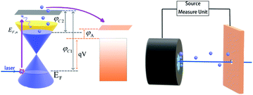 |
| | Fig. 1 The process of PETE in GA surface, where EF is the Fermi level of graphene, EF,n is Quasi Fermi Level of graphene after irradiated by laser, φC1 is graphene's work function, φC2 is the work function of graphene that in unstable state under the laser effect. φA is anode work function, qV is the difference of Fermi energy levels between cathode and anode. | |
2. Experimental
GA was prepared in the following steps. Firstly, High-purity GO was dispersed in deionized water by the ultrasonic wave and then put into a high-pressure reactor at 150 °C for 12 h to obtain graphene hydrogel. Subsequently, the graphene hydrogel was moved to the natural environment for 24 h to remove the surface moisture. Finally, GA was obtained by drying the graphene hydrogel in the vacuum freeze device. The diameter of GA is 12 mm and the height is 5 mm.
3D graphene powder (GP) and 2D graphene (2DG) were prepared as the control group, in which GP was soaked in absolute ethanol and coated on a 10 mm × 10 mm copper sheet, the thickness is 1 mm. 2DG was produced by Suzhou Tanfeng Graphene Co., Ltd. It was deposited on a 10 mm × 10 mm copper sheet by CVD with a thickness of 0.3 nm.
To construct the PETE device, a vacuum container was self-designed as shown in Fig. 2(a). There are two four-interfaces electrodes on the side of the container to ensure that the electrical signals can be derived external. The container is connected with the vacuum system to achieve a high vacuum level. Fig. 2(b) shows the picture of the container and GA is placed in the center of the container. The structure of PETE devices adopts the hole-digging type as shown in Fig. 2(c) and (d). Cu sheet was folded into a semi-open structure to collect the electrons. The material of the base was polytetrafluoroethylene (PTEF) to ensure insulation, and plastic screws were used to fix the cathode and anode. Cathode and electrodes were connected by wires to export electrical signals. The standard model of PETE was calculated to explain the variation trend of current in the experiment.
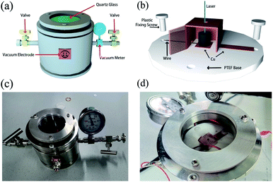 |
| | Fig. 2 (a) Schematic diagram of vacuum container, (b) schematic diagram of cathode and anode structure, (c) photo of vacuum container, (d) photo of the device after being put into the container. | |
The structure of GO and GA were measured by Fourier-transform infrared (FT-IR) spectroscopy (IRTracer-100, SHIMADZU) in the range of 400 to 4000 cm−1. The reduction degree of GA was characterized by X-ray photoelectron spectroscopy (XPS, ESCALAB 250XI+, Thermo Fisher Scientific). X-ray diffraction (XRD, Rigaku D/MAX 2500 V) patterns were recorded with a scan range from 5° to 90° and a scan rate of 10° min−1. The morphologies of GO and GA were investigated by transmission electron microscope (TEM, TECNAI G2 F30, FEI) and scanning electron microscopy SEM (Sigma-300, ZEISS). When the vacuum in the container reached 10−4 Pa, GA, GP and 2DG were irradiated by the laser with the wavelength of 450 nm at different power, and I–t curves of the PETE device were measured by the Source Measure Unit (2400, Keithley).
3. Results and discussion
3.1 FTIR analysis
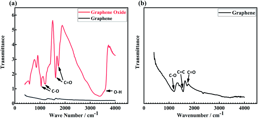
Fig. 3(a) shows the FTIR spectra of GA and GO. GO has C–O stretching vibration peaks at 1047 cm−1 and 1207 cm−1,27 C![[double bond, length as m-dash]](https://www.rsc.org/images/entities/char_e001.gif) O stretching vibration peaks at 1628 cm−1 and 1730 cm−1,27 and O–H stretching vibration peak at 3383 cm−1.28 By comparison, GA shows lower transmittance, and the enlarged spectrum is illustrated in Fig. 3(b). It can be seen that the O–H absorption peak in GO disappears after the reduction reaction, and CO absorption peaks were greatly weakened. Meanwhile, CC stretching vibration peak at 1568 cm−1 is observed, which is assigned to the characteristic vibration mode of graphene.29
O stretching vibration peaks at 1628 cm−1 and 1730 cm−1,27 and O–H stretching vibration peak at 3383 cm−1.28 By comparison, GA shows lower transmittance, and the enlarged spectrum is illustrated in Fig. 3(b). It can be seen that the O–H absorption peak in GO disappears after the reduction reaction, and CO absorption peaks were greatly weakened. Meanwhile, CC stretching vibration peak at 1568 cm−1 is observed, which is assigned to the characteristic vibration mode of graphene.29
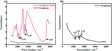 |
| | Fig. 3 (a) FTIR curve of graphene and graphene oxide, (b) the enlarged curve of graphene. | |
3.2 The reduction degree of GA
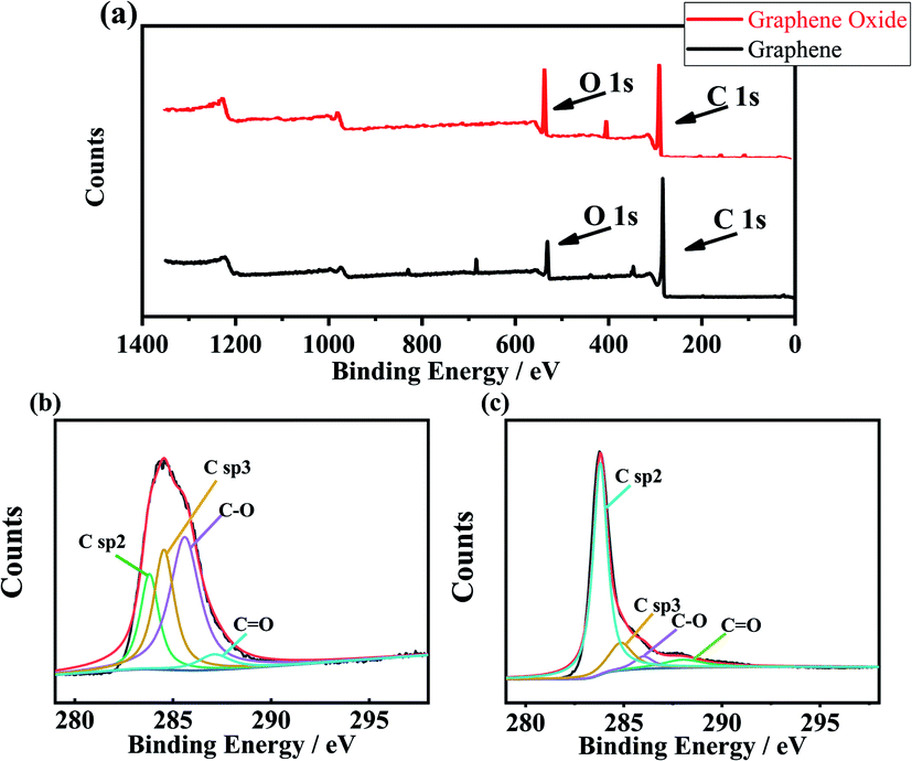
XPS spectra of GO and GA are shown in Fig. 4. Fig. 4(a) is the survey spectra of GA and GO. The O1s peak of GA decreased significantly. Fig. 4(b) and (c) show the high-precision C 1s region of GO and GA respectively. From Fig. 4(a), the peak of C sp2, C sp3, C–O bond and CO bond was founded at the binding energy of 283.8 eV, 284.54 eV,30,31 285.6 eV and 287.2 eV.32 The atomic concentration can be obtained from the peak area ratio, the atomic concentration of the C–O bond was the highest, it was 45.99 at%, C sp3, and C sp2 were 28.90 at% and 20.26% respectively. In Fig. 4(b), C sp2, C sp3, C–O bond and CO bond were at 283.8 eV, 284.8 eV, 286.0 eV and 287.9 eV respectively. Compared with GO, the atomic concentration of C sp2 in GA increased significantly to 70.73 at%, the atomic concentration of C sp3 decreased to 15.74%, C–O decreased to 5.78%, and the atomic concentration of CO bond remained basically unchanged at 5.97%.
 |
| | Fig. 4 XPS spectra of GO and GA, (a) is the XPS survey of GO and GA, (b) is the C 1s scan of GO, (c) is the C 1s scan of GA. | |
3.3 XRD characterization of GO and GA
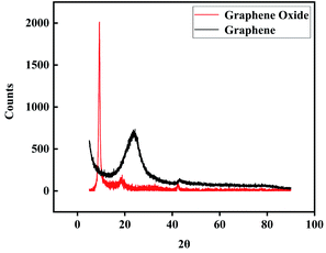
The XRD spectra of GO and GA are shown in Fig. 5, GO that was not dispersed by ultrasound appeared a (0 0 2) strong diffraction peak at 2θ = 9.30(ref. 33 and 34) and its FWHM was 0.566° (10) diffraction peak at 2θ = 42.85 shows that GO and GA have short-range order features.34 Bragg's equation and Scherrer's equation were used to calculate layer (d) spacing and thickness (H) of GO respectively. As a result, the d was about 1.03 nm and the H was about 0.85 nm, which indicates that most GO sheets were single-layer. After thermal reduction, GA showed the characteristics of an amorphous state, it may be related to the curling deformation of graphene sheets during the reaction.
 |
| | Fig. 5 XRD spectra of GO and GA. | |
3.4 Electron microscope characterization of GO and GA
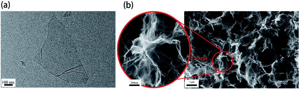
Fig. 6(a) shows the TEM morphology of GO. After ultrasonic dispersion, monolayer GO is clearly seen with the diameter of 650–800 nm. When GO was reduced to graphene in water, graphene fragments were automatically assembled into graphene hydrogels by van der Waals force. Fig. 6(b) shows the assembled network structure of GA, and the thickness of graphene fragments is still small. The network structure can reduce the light reflectivity on the cathode surface, resulting a high light-trapping performance.35 Besides, the network structure improves the conductivity of cathode by reducing the electrons loss during transport.
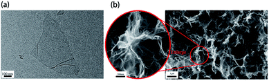 |
| | Fig. 6 (a) TEM morphology of GO, (b) SEM morphology of GA. | |
3.5 Photon-enhanced thermionic emission response of GA
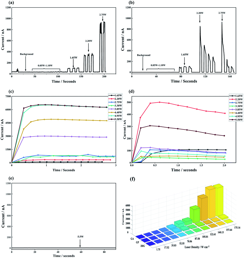
When the GA, GP and 2DG was irradiated by different power 450 nm laser, electrons escaped from the cathode surface. The curve collected by the measure unit was shown in Fig. 7(a)–(e). Fig. 7(a) and (c) show the I-t curve of GA under different powers. Fig. 7(b) and (d) show the I-t curve of GP under different powers. Fig. 7(a) and (c) show that when the laser power is lower than 1.65 W, the anode could hardly receive any electrons. When the laser power reaches 1.65 W, the source measure unit detected an obvious current, which was 98 nA, and the response time was less than 0.2 seconds. With the increase of laser power, the PETE current increased rapidly until up to 6290 nA, and in that case, the laser power was 4.95 W. Fig. 7(b) and (d) indicate that under the irradiation of lower laser intensity (1.65 W), GP had the same performance as GA. It is the first time that GP has been found to have the ability of PETE. When the laser intensity is 1.65w, the PETE current is 96 nA, which is roughly the same as GA. With the increase of laser power, the PETE current of GP does not increase regularly and it even decreased when the laser power is 3.30 W. The reason for this phenomenon may be that graphene will be pushed under laser irradiation, while the structure of GP is relatively loose and cannot maintain a stable shape when it was irradiated. Fig. 7(e) shows that 2DG can hardly generate PETE current at the laser power of 5.5 W.
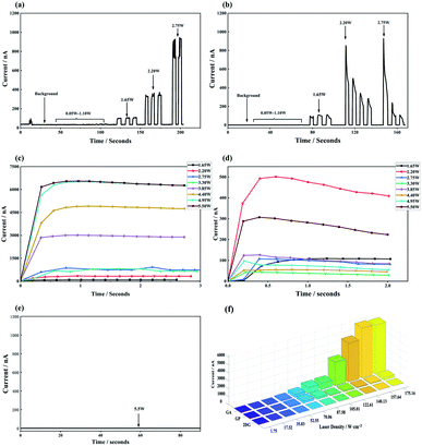 |
| | Fig. 7 (a) Is the I–t curve of GA, (b) is the I–t curve of GP, (c) and (d) is the I–t curve of GA and GP in different laser power respectively. (e) Is the I–t curve of 2DG, (f) is the relationship between PETE current and laser density. | |
To show the relationship between laser and current intuitively, the laser power was conversed to energy density as the abscissa according to the laser illumination square, and the current was the ordinate, as shown in Fig. 7(f). Fig. 7(f) shows that the PETE performance and stability of GA are better than GP and 2DG. Under the irradiation of the high-intensity laser, the emission capacity of GA can increase steadily. When the density of 450 nm laser was lower than 35 W cm−2, the thermoelectrons did not have enough energy to overcome the work function of GA and GP.37 This phenomenon was similar to the previously reported.18 In early work, graphene was irradiated by concentrate light by a solar simulator. Although the total power of incident light was about 3 W, which was much higher than the threshold laser power: 1.65 W, the source measure unit cannot defect any current. Compared with GaAs, GA needs more energy to emit electrons in the PETE process. GaAs only need 6.4W cm−2.36 In addition to the work function of the cathode, two factors are affecting the light threshold of electrons emission: the first point is that graphene does not have bandgap, which makes the photo-thermal conversion efficiency of graphene low. According to theory, the optimum bandgap of the cathode material is 1.4 eV.1 Another point is that Cs steam is not used in this experiment, because the adsorption of Cs atoms on the cathode surface can effectively reduce the work function and space charge effect.36
3.6 Energy conversion efficiency of the device
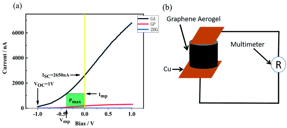
When the laser power was 5.5 W and the PETE current tended to be stable, bias voltage was put on the device and the current–bias curve was obtained by the source measure unit. The curve is shown in Fig. 8(a). Short-circuit current of GA in the device was 2650 nA. When the reverse voltage was −1 V, the current disappeared. It can be concluded that the open-circuit voltage of the device was 1 V. According to the formula (1) of photovoltaic cells:where Pmax is the maximum power of the solar cell, VOC is the open-circuit voltage, ISC is the short-circuit current, and FF is the fill factor.
 |
| | Fig. 8 (a) The I–V curve after bias voltage is applied to the source meter, (b) the schematic diagram of GA resistance test. | |
When the bias was −0.387 V, the green region of Fig. 8(a) was the largest. In that case, the filling factor was 0.169, the power of the device was 448 nW and the laser power was 5.5 W and the device efficiency is 8.14 × 10⁻⁶%. The efficiency of the device can also be calculated according to the following formula (2):1,36
| | |
PPETE = (JC − JA)[(φC − φA)/e + Vbias]
| (2) |
where
PPETE is the output power of the device,
JC is the current density of electrons emitted from the cathode to the anode,
JA is the current density of electrons emitted from the anode to the cathode, and
Vbias is the bias voltage,
φC and
φA is the work function of the cathode and anode respectively. According to the work function of graphene is 4.89–5.16 eV,
38 the
PPETE was about 737–1040 nW, and the device efficiency was 1.89–1.34 × 10
−5%. The main factor of low efficiency is the massive resistance of GA. The resistance of GA from bottom to top is 143 kΩ (the measurement method is shown in
Fig. 8(b). The bias–scan curve of GP device is similar to GA. According to formula (
1), the output power of GP device was 29.54 nW and the conversion efficiency was 5.18 × 10
−7%. Since there was no current detected in 2DG device, the current does not change with the bias and its value is near 0 nA.
A high resistance will lead to a great loss of electrons in the process of transmission inside the cathode material.38 If graphene is made thinner, the loss will be avoided, which can improve the efficiency by 5 orders of magnitude. At the same time, GA and the copper plate do not form a perfect contact, which is also an important factor affecting efficiency.39
3.7 Explanation of current variation of the devices
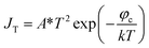
There is a unique phenomenon in the PETE I–t curve: The current decreased slightly after the laser irradiate GA for a few seconds, as shown in Fig. 9. PETE's standard model1,40 may explain this variation. In this model, the ability of the cathode to emit electrons depends on the population in the conduction band of the cathode n:| |
 | (3.1) |
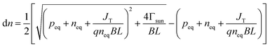
where A* is the Richardson constant, T is the cathode temperature, k is the Boltzmann constant, neq is the equilibrium population in the conduction band. Under the laser irradiation, the electrons concentration of the conduction band isdn is the nonequilibrium population. According to the derivation,31 dn can be expressed as:| |
 | (3.3) |
where peq is the concentration of holes in equilibrium,41 L is the thickness of the cathode, q is the single-electron charge, Γsun is the flux of photons per area, JT is the current density of thermionic emission, B is the rate of radiative recombination, it can be expressed as formula (3.4):| |
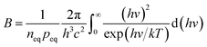 | (3.4) |
| |
 | (3.5) |
where hv is photon energy, c is the speed of the light. The curve of JC can be obtained according to formula (3.1) to (3.5), the theoretical value of PPETE can be obtained by putting JC into formula (2), and the energy conversion efficiency of the device η can be calculated by formula (3.6)| |
 | (3.6) |
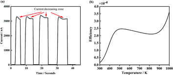 |
| | Fig. 9 (a) Is the I–t curve of GA irradiate by 5.5 W laser, (b) is the theoretical efficiency curve of the PETE devices. | |
The results are shown in Fig. 9(b). According to the PETE's model, the efficiency of the device increases rapidly with the increase of temperature. Meanwhile, the Fermi level of cathode material increases slightly, resulting in the decline of the efficiency.31 When the temperature further increases, pure thermionic emission dominates and the efficiency improves again.
4 Conclusions
Graphene aerogel was prepared by hydrothermal reduction of GO with a diameter of about 650–800 nm. In the PETE experiment, the electron emission ability of GA was significantly affected by the laser density. When the laser intensity of 450 nm was greater than 35 W cm−2, the PETE current can be detected by the source unit. In conclusion, the density of light is an important parameter affecting the emission ability of the cathode. The output power of the device was about 448–1040 nW, and the conversion efficiency was 8.1 × 10⁻⁶ to 1.8 × 10⁻⁵%, it depends on calculation methods. Low efficiency is mainly caused by the loss of electrons in the cathode. If graphene can be deposited on the substrate by advanced method, it can form good contact with the load and the resistance will drop by 5 orders of magnitude, the efficiency may get promotion obviously. Therefore, maybe graphene is not the best choice, the optimization of cathode structure is still a way worthy of exploration. In addition, GP also shows the ability of PETE, although it is not stable compared with GA, which may make graphene used in a wider use.
Conflicts of interest
There are no conflicts to declare.
Acknowledgements
This work was supported by the National Natural Science Foundation of China (61474030). The authors thank Cai Hangchuan and his research group for their assistance in equipment. The authors appreciate Fiona Chang for her modification.
References
- J. W. Schwede, I. Bargatin, D. C. Riley, B. E. Hardin, S. J. Rosenthal, Y. Sun, F. Schmitt, P. Pianetta, R. T. Howe and Z.-X. Shen, Nat. Mater., 2010, 9, 762–767 CrossRef CAS PubMed.
- Y. Lee, C. Park, N. Balaji, Y. J. Lee and V. A. Dao, Isr. J. Chem., 2015, 55, 1050–1063 CrossRef CAS.
- M. Sui, Y. Chu and R. Zhang, J. Phys.: Conf. Ser., 2021, 1907, 012026 CrossRef CAS.
- L. C. Andreani, A. Bozzola, P. Kowalczewski, M. Liscidini and L. Redorici, Adv. Phys.: X, 2019, 4, 1548305 CAS.
- D. H. Levi, M. A. Green, Y. Hishikawa, E. D. Dunlop, J. Hohl-Ebinger and A. W. Ho-Baillie, Prog. Photovoltaics, 2017, 26, 3–12 Search PubMed.
- A. Kribus and G. Segev, J. Opt., 2016, 18, 073001 CrossRef.
- G. Segev, Y. Rosenwaks and A. Kribus, Sol. Energy Mater. Sol. Cells, 2012, 107, 125–130 CrossRef CAS.
- G. Segev, Y. Rosenwaks and A. Kribus, Sol. Energy Mater. Sol. Cells, 2015, 140, 464–476 CrossRef CAS.
- E. Rahman and A. Nojeh, Nat. Commun., 2021, 12, 1–9 CrossRef PubMed.
- L. Liu, Y. Diao and S. Xia, J. Mater. Sci., 2019, 54, 5605–5614 CrossRef CAS.
- K. Sahasrabuddhe, J. W. Schwede, I. Bargatin, J. Jean, R. T. Howe, Z.-X. Shen and N. A. Melosh, J. Appl. Phys., 2012, 112, 094907 CrossRef.
- N. Kumar, R. Salehiyan, V. Chauke, O. J. Botlhoko, K. Setshedi, M. Scriba, M. Masukume and S. S. Ray, FlatChem, 2021, 100224 CrossRef CAS.
- S. Horiuchi, T. Gotou, M. Fujiwara, T. Asaka, T. Yokosawa and Y. Matsui, Appl. Phys. Lett., 2004, 84, 2403–2405 CrossRef CAS.
- X. Zhang, Y. S. Ang, J.-Y. Du, J. Chen and L. K. Ang, J. Cleaner Prod., 2020, 242, 118444 CrossRef CAS.
- M. Sajibul, A. Bhuyan, M. N. Uddin, M. M. Islam, F. A. Bipasha and S. S. Hossain, Int. Nano Lett., 2016, 6, 65 CrossRef.
- D. C. Marcano, D. V. Kosynkin, J. M. Berlin, A. Sinitskii, Z. Sun, A. Slesarev, L. B. Alemany, W. Lu and J. M. Tour, ACS Nano, 2010, 4, 4806–4814 CrossRef CAS PubMed.
- Y. Wu, N. Yi, L. Huang, T. Zhang, S. Fang, H. Chang, N. Li, J. Oh, J. A. Lee and M. Kozlov, Nat. Commun., 2015, 6, 1–9 Search PubMed.
- T. Zhang, H. Chang, Y. Wu, P. Xiao, N. Yi, Y. Lu, Y. Ma, Y. Huang, K. Zhao and X.-Q. Yan, Nat. Photonics, 2015, 9, 471–476 CrossRef CAS.
- C.-H. Liu, N. M. Dissanayake, S. Lee, K. Lee and Z. Zhong, ACS Nano, 2012, 6, 7172–7176 CrossRef CAS PubMed.
- D. Zhi, T. Li, J. Li, H. Ren and F. Meng, Composites, Part B, 2021, 211, 108642 CrossRef CAS.
- K.-Q. Lu, L. Yuan, X. Xin and Y.-J. Xu, Appl. Catal., B, 2018, 226, 16–22 CrossRef CAS.
- K.-Q. Lu, X. Xin, N. Zhang, Z.-R. Tang and Y.-J. Xu, J. Mater. Chem. A, 2018, 6, 4590–4604 RSC.
- M.-Q. Yang, N. Zhang, Y. Wang and Y.-J. Xu, J. Catal., 2017, 346, 21–29 CrossRef CAS.
- Y. Chen, X. Xie, X. Xin, Z.-R. Tang and Y.-J. Xu, Acs Nano, 2018, 13, 295–304 CrossRef PubMed.
- G. Zheng, PhD thesis, Zhejiang University, 2019 Search PubMed.
- J. Garcia-Merino, L. Fernández-Izquierdo, R. Villarroel and S. Hevia, J. Materiomics, 2021, 7, 271–280 CrossRef.
- S. Chaiyakun, N. Witit-Anun, N. Nuntawong, P. Chindaudom, S. Oaew, C. Kedkeaw and P. Limsuwan, Procedia Eng., 2012, 32, 759–764 CrossRef.
- M. Strankowski, D. Włodarczyk, Ł. Piszczyk and J. Strankowska, J. Spectrosc., 2016, 2016, 1–6 CrossRef.
- V. Loryuenyong, K. Totepvimarn, P. Eimburanapravat, W. Boonchompoo and A. Buasri, Adv. Mater. Sci. Eng., 2013, 2013, 923403 Search PubMed.
- L. Stobinski, B. Lesiak, A. Malolepszy, M. Mazurkiewicz, B. Mierzwa, J. Zemek, P. Jiricek and I. Bieloshapka, J. Electron Spectrosc. Relat. Phenom., 2014, 195, 145–154 CrossRef CAS.
- R. Wang, K.-Q. Lu, F. Zhang, Z.-R. Tang and Y.-J. Xu, Appl. Catal., B, 2018, 233, 11–18 CrossRef CAS.
- R. Al-Gaashani, A. Najjar, Y. Zakaria, S. Mansour and M. Atieh, Ceram. Int., 2019, 45, 14439–14448 CrossRef CAS.
- L. Stobinski, B. Lesiak, A. Malolepszy, M. Mazurkiewicz, B. Mierzwa, J. Zemek, P. Jiricek and I. Bieloshapka, J. Electron Spectrosc. Relat. Phenom., 2014, 195, 145–154 CrossRef CAS.
- S. N. Alam, N. Sharma and L. Kumar, Graphene, 2017, 6, 1–18 CrossRef CAS.
- J. Buencuerpo, J. M. Llorens, P. Zilio, W. Raja, J. Cunha, A. Alabastri, R. P. Zaccaria, A. Martí and T. Versloot, Opt. Express, 2015, 23, A1220–A1235 CrossRef CAS PubMed.
- W. Tang, PhD thesis, Xian Institute of Optics & Precision Mechanics Chinese Academy of Sciences, 2014 Search PubMed.
- S. M. Song, J. K. Park, O. J. Sul and B. J. Cho, Nano Lett., 2012, 12, 3887–3892 CrossRef CAS PubMed.
- M. Girolami, L. Criante, F. Di Fonzo, S. L. Turco, A. Mezzetti, A. Notargiacomo, M. Pea, A. Bellucci, P. Calvani and V. Valentini, Carbon, 2017, 111, 48–53 CrossRef CAS.
- F. Rana, P. A. George, J. H. Strait, J. Dawlaty, S. Shivaraman, M. Chandrashekhar and M. G. Spencer, Phys. Rev. B, 2009, 79, 115447 CrossRef.
- H. Che, Master thesis, Zhejiang University, 2019 Search PubMed.
- S. M. Sze and K. K. Ng, Physics of Semiconductor Devices, John Wiley & Sons, Inc., Hoboken, New Jersey, 2007 Search PubMed.
|
| This journal is © The Royal Society of Chemistry 2022 |
Click here to see how this site uses Cookies. View our privacy policy here. 
 Open Access Article
 This Open Access Article is licensed under a Creative Commons Attribution-Non Commercial 3.0 Unported Licence