
 Open Access Article
 This Open Access Article is licensed under a Creative Commons Attribution-Non Commercial 3.0 Unported Licence
Layered post-transition-metal dichalcogenide SnGe2N4 as a promising photoelectric material: a DFT study
Vo D. Data and
Tuan V. Vu *bc
*bc
aGroup of Computational Physics and Simulation of Advanced Materials, Institute of Applied Technology, Thu Dau Mot University, Binh Duong Province, Vietnam. E-mail: voduydat@tdmu.edu.vn
bDivision of Computational Physics, Institute for Computational Science, Ton Duc Thang University, Ho Chi Minh City, Vietnam. E-mail: vuvantuan@tdtu.edu.vn
cFaculty of Electrical & Electronics Engineering, Ton Duc Thang University, Ho Chi Minh City, Vietnam
First published on 1st April 2022
Abstract
First-principles calculations were performed to study a novel layered SnGe2N4 compound, which was found to be dynamically and thermally stable in the 2H phase, with the space group P![[6 with combining macron]](https://www.rsc.org/images/entities/char_0036_0304.gif) m2 and lattice constant a = 3.143 Å. Due to its hexagonal structure, SnGe2N4 exhibits isotropic mechanical properties on the x–y plane, where the Young’s modulus is 335.49 N m−1 and the Poisson’s ratio is 0.862. The layered 2H SnGe2N4 is a semiconductor with a direct band gap of 1.832 eV, allowing the absorption of infrared and visible light at a rate of about 104 cm−1. The DOS is characterized by multiple high peaks in the valence and conduction bands, making it possible for this semiconductor to absorb light in the ultraviolet region with an even higher rate of 105 cm−1. The band structure, with a strongly concave downward conduction band and rather flat valence band, leads to a high electron mobility of 1061.66 cm2 V−1 s−1, which is substantially greater than the hole mobility of 28.35 cm2 V−1 s−1. This difference in mobility is favorable for electron–hole separation. These advantages make layered 2H SnGe2N4 a very promising photoelectric material. Furthermore, the electronic structure of 2H SnGe2N4 responds well to strain and an external electric field due to the specificity of the p–d hybridization, which predominantly constructs the valence bands. As a result, strain and external electric fields can efficiently tune the band gap value of 2H SnGe2N4, where compressive strain widens the band gap, meanwhile tensile strain and external electric fields cause band gap reduction. In particular, the band gap is decreased by about 0.25 eV when the electric field strength increases by 0.1 V Å−1, making a semiconductor–metal transition possible for the layered SnGe2N4.
m2 and lattice constant a = 3.143 Å. Due to its hexagonal structure, SnGe2N4 exhibits isotropic mechanical properties on the x–y plane, where the Young’s modulus is 335.49 N m−1 and the Poisson’s ratio is 0.862. The layered 2H SnGe2N4 is a semiconductor with a direct band gap of 1.832 eV, allowing the absorption of infrared and visible light at a rate of about 104 cm−1. The DOS is characterized by multiple high peaks in the valence and conduction bands, making it possible for this semiconductor to absorb light in the ultraviolet region with an even higher rate of 105 cm−1. The band structure, with a strongly concave downward conduction band and rather flat valence band, leads to a high electron mobility of 1061.66 cm2 V−1 s−1, which is substantially greater than the hole mobility of 28.35 cm2 V−1 s−1. This difference in mobility is favorable for electron–hole separation. These advantages make layered 2H SnGe2N4 a very promising photoelectric material. Furthermore, the electronic structure of 2H SnGe2N4 responds well to strain and an external electric field due to the specificity of the p–d hybridization, which predominantly constructs the valence bands. As a result, strain and external electric fields can efficiently tune the band gap value of 2H SnGe2N4, where compressive strain widens the band gap, meanwhile tensile strain and external electric fields cause band gap reduction. In particular, the band gap is decreased by about 0.25 eV when the electric field strength increases by 0.1 V Å−1, making a semiconductor–metal transition possible for the layered SnGe2N4.
1 Introduction
Nowadays, the quick development of modern technology delivers wonderful solutions to human life while also causing excessive energy consumption, natural resource depletion, and severe pollution. As a result, new devices must be more powerful and energy-efficient, with advanced materials at the heart of the solution. Two-dimensional (2D) materials have been widely considered as promising candidates for this task due to a wide range of excellent features, including good thermal conductivity, tunable band gaps, high charge carrier mobility, surface activity, electronic anisotropy, and ultrahigh specific surface area.1–8 As a result, several two-dimensional structures, including MoS2/SiC heterostructures, PdSeO3 monolayers, COFs, AgBiP2Se6 monolayers, phosphorene nanoribbons, and carbon-doped BN nanosheets, have been demonstrated to be ideal for solar energy conversion and photocatalysis.9–14 Other 2D materials, such as MoS2, hexagonal-BN, WSe2–MoS2, MoSe2, WSe2, and hybrid 2D material heterostructures, are also very promising for the next generation of transistors,15–20 allowing for the miniaturization and integration of nano-electronic devices.Despite extensive theoretical research, most 2D materials are difficult to produce experimentally. As a result of Hong’s successful exfoliation of MoSi2N4 monolayers,21 a series of investigations on the novel 2D material family with the formula MX2Y4 (M = transition metal, X = Ge or Si, and Y = As, P, or N) has been performed, in which the MY2 in the 2H phase is sandwiched between two buckled honeycomb XY layers.22 On the one hand, most M2Y4 monolayers have the same advantageous properties, such as high charge carrier mobility and good tensile strength. On the other hand, the ability to modify the 2H-MY2 and XY layers in the sandwiched structure of MX2Y4 results in a wide range of excellent properties. MoSi2N4 and WSi2N4 monolayers, for example, are excellent candidates for optoelectronic and photovoltaic applications21,23 due to their high visible light absorption, good charge carrier mobility, and suitable band structure. Likewise, the intrinsic piezoelectric monolayers CrSi2N4, VSi2P4, and VSi2N4 are very promising for spintronic devices.23,24 Furthermore, numerical studies25 show that monolayer and bilayer MoSi2Z4 (Z = P, As) exhibit outstanding structural stability, isotropic mechanical characteristics, a low bandgap, good carrier mobilities, exceptional optical absorption, superior photon responsivity, and external quantum efficiency.
While most d-block metals are theoretically predicted to form MoSi2N4-like structures,23,26,27 analogous formations containing post-transition metals (p-block metals) have not yet been investigated. It is worth noting that the majority of p-block elements have been demonstrated to form stable 2D phases with lattice structures similar to that of graphene.28 The post-transition metal Sn, in particular, has been shown to exist in a buckled hexagonal structure with mechanical stability and high photothermal activity.29–31 Furthermore, Sn monolayers can combine with other 2D materials like boron nitride and graphene to form multi-plane structures similar to MoSi2N4-like monolayers.32,33 To extend the search for new 2D materials, the post-transition metal Sn was designed to replace Mo in the SnGe2N4 monolayer, the characteristics of which were investigated in this paper using first-principles calculations. Also explored are the impacts of strain and external electric fields on the characteristics of layered SnGe2N4.
2 Methodology
The layered SnGe2N4 lattice structure was built in the 2H phase with the space group Pm2, because MoSi2N4 was experimentally discovered to crystallize in the 2H phase,21 and most of the compounds in the MoSi2N4 family have also been confirmed theoretically to be more stable in the 2H phase than in the 1T phase.23,34–37 Taking into account the atomic radii of the constituent atoms Mo, Si, and N, the initial lattice parameters were established to be a = b = 3.143 Å, and c = 30 Å to avoid interaction between monolayers due to the periodicity. The equilibrium structure of SnGe2N4 was obtained by relaxing the present atomic model using the generalized gradient approximation specified by Perdew–Burke–Ernzerhof (PBE)38 and implemented in the Vienna ab initio simulation package (VASP).39 The semi-empirical function DFT-D3![[thin space (1/6-em)]](https://www.rsc.org/images/entities/char_2009.gif) 40 was also used to account for the weak van der Waals interactions between the H-SnN2 and GeN planes. The pseudopotentials, which were used to represent the interaction between particles, including ions and valence electrons of the N-2s22p3, Sn-4d105s25p2 and Ge-3d104s24p2 orbitals, were constructed using the projected augmented wave (PAW) approach,41 where the scale relativistic effects were included. All cell periodic functions were expanded using a plane wave basic set with a cut off energy of 500 eV and a Gaussian smearing parameter of 0.05. The self-consistent calculations were carried out until the difference in total energies was less than 1 meV, the force acting on ions smaller than 0.01 eV Å−1, and the electron energy less than 10−4 eV. It is worth noting that a 15 × 15 × 1 k-point mesh was employed for both structural optimization and calculating the system’s characteristics. Furthermore, the PBE + SOC method was used to include the spin–orbit interaction, and the hybrid function described by Heyd–Scuseria–Ernzerhof (HSE06)42 was used to improve the system’s band gap. A 4 × 4 × 1 supercell was constructed to calculate the phonon dispersion of 2H SnGe2N4, where the PHONOPY package and finite displacement method as implemented in VASP43 were used.
40 was also used to account for the weak van der Waals interactions between the H-SnN2 and GeN planes. The pseudopotentials, which were used to represent the interaction between particles, including ions and valence electrons of the N-2s22p3, Sn-4d105s25p2 and Ge-3d104s24p2 orbitals, were constructed using the projected augmented wave (PAW) approach,41 where the scale relativistic effects were included. All cell periodic functions were expanded using a plane wave basic set with a cut off energy of 500 eV and a Gaussian smearing parameter of 0.05. The self-consistent calculations were carried out until the difference in total energies was less than 1 meV, the force acting on ions smaller than 0.01 eV Å−1, and the electron energy less than 10−4 eV. It is worth noting that a 15 × 15 × 1 k-point mesh was employed for both structural optimization and calculating the system’s characteristics. Furthermore, the PBE + SOC method was used to include the spin–orbit interaction, and the hybrid function described by Heyd–Scuseria–Ernzerhof (HSE06)42 was used to improve the system’s band gap. A 4 × 4 × 1 supercell was constructed to calculate the phonon dispersion of 2H SnGe2N4, where the PHONOPY package and finite displacement method as implemented in VASP43 were used.
3 Stability and elastic properties
The optimized hexagonal structure of 2H SnGe2N4, as shown in Fig. 1(a), is characterized by lattice parameters a = b = 3.143 Å, which are close to the lattice constants of CrGe2N4 = 2.98 Å, MoGe2N4 = 3.04 Å, and WGe2N4 = 3.04 Å23. Like other compounds in the 2D MoSi2N4 family,44,45 the layered SnGe2N4 is constructed by a 2H-SnN2 monolayer vertically stacked between two buckled hexagonal GeN layers such that each Sn atom bonds with six Ge atoms, forming a trigonal prism. The lengths of the Sn–N and Ge–N bonds are 2.2 Å and 1.9 Å, respectively. These bond lengths are about 7% larger than the corresponding values of the spinel SnGe2N4, which were calculated by the LDA method in a previous study by Ching et al.46 It is worth noting that the bond lengths of layered SnGe2N4 were computed using the PBE approach; nonetheless, the LDA and PBE methods reveal bond lengths that differ just slightly.47 Therefore, the bonding nature of 2H SnGe2N4 is expected to be more covalent than the one in spinel SnGe2N4. This assumption is confirmed by the fact that the Sn–N and Ge–N bond lengths in 2H SnGe2N4 are longer than the sum of the corresponding constituent ionic radii of Sn, Ge, and N, which are 1.32 Å, 1.14 Å, and 0.54 Å, respectively.48 The electron localization function (ELF) of layered SnGe2N4 on the (1 1 0) cross-section is depicted in Fig. 1(b), where fully localized (1.0) and delocalized (0.5) electrons are denoted by red and green areas, respectively, while the blue region (0.0) denotes very low electron density. The red zone is largely focused on the N atoms, indicating that electrons are strongly localized around these atoms. Meanwhile, a considerable spread of delocalized electrons can be seen in the green areas connecting the N atoms to Sn atoms or Ge atoms. As a result, the layered SnGe2N4 exhibits covalent bonding properties. | ||
| Fig. 1 (a) Top and side views, (b) electron localization function (ELF) of optimized 2H SnGe2N4. Time-dependence of (c) total energy and (d) temperature in 2H SnGe2N4 at 300 K, (e) phonon dispersion, and (f) work function, depending on the distance along the z-axis, of 2H SnGe2N4. | ||
Because no previous research has indicated the existence of 2H SnGe2N4, its stability must be examined. The phonon dispersion along the highly symmetric path Γ–M–K–Γ in the Brillouin zone was conducted to estimate the dynamical stability of 2H SnGe2N4. As illustrated in Fig. 1(e), all 21 phonon branches (corresponding to 7 atoms in a unit cell) are positive, demonstrating the dynamic stability of 2H SnGe2N4. The acoustic branches are characterized by gradual slopes, indicating a moderate group velocity, elastic modulus and median melting point of 2H SnGe2N4. It is expected that heat transferred by the acoustic branches is not interrupted by the optical branches due to the existence of a frequency gap between the two types of phonon branches. The thermal stability was estimated by heating the 2H SnGe2N4 to 300 K for 6 ps using ab initio molecular dynamics (AIMD). The total energy of the 2H SnGe2N4 does not vary drastically over the temperature fluctuation for 6 ps, as illustrated in Fig. 1(c and d), suggesting the thermal stability of this structure. The energy–time graph in Fig. 1(c) also shows certain local minima owing to modest structural perturbations that swiftly recover to the equilibrium 2H SnGe2N4 structure.
To analyze the mechanical strength of 2H SnGe2N4, strain was applied the compound to measure the Young’s modulus Y(θ) and Poisson’s ratio ν(θ), where θ is the in-plane angle between the lattice vector and the direction of the strain. The elastic constants C11, C12 and C66 were calculated to determine Y(θ) and ν(θ) as follows:49
 | (1) |
 | (2) |
As shown in Fig. 2, the symmetric circles of the Young’s modulus and Poisson’s ratio suggest isotropic mechanical characteristics of SnGe2N4 in the x–y plane. As the Young’s modulus represents the slope of the stress–strain curve, the layered SnGe2N4 with a Young’s modulus of 335.49 N m−1, as presented in Table 1, is expected to be more brittle than MoSi2As4 and MoSi2P4, whose Young’s moduli are about 118–138 N m−1.25 At the same time, it is more ductile than other materials in the same family, such as MoSi2N4 and WSi2N4, whose Young’s modulus is 500–600 N m−1.37,50 Meanwhile, the Poisson’s ratio of 0.286 implies that 2H SnGe2N4 expands perpendicularly to the strain direction.
 | ||
| Fig. 2 Dependence of (a) Young’s modulus Y(θ) and (b) Poisson’s ratio μ(θ) on the in-plane angle θ calculated for 2H SnGe2N4. | ||
| a | dSn–N | dGe–N | Δh | EPBEg | EPBE+SOCg | EHSE06g | C11 | C12 | C66 | Y2D | ν |
|---|---|---|---|---|---|---|---|---|---|---|---|
| 3.143 | 2.203 | 1.908 | 7.443 | 0.934 | 0.932 | 1.832 | 365.417 | 104.569 | 130.424 | 335.493 | 0.286 |
Aside from light absorption, another significant property of photoelectric materials is their work function.51–53 The work function is the amount of energy required to release an electron from the surface of a substance and transfer it to vacuum. As a result, the difference between the vacuum electrostatic potential and the Fermi level is equivalent to this energy.54 The predicted work function Φ of 2H SnGe2N4 is 6.216 eV, as shown in Fig. 1(f), which is comparable to the work functions of layered transition metal dichalcogenides (ZrSe2, HfSe2, NbSe2, 1T-TaS2, 2H-TaS2, MoS2, MoSe2, SnS2 and SnSe2), which range from 5 to 7.4 eV.55 The work function of roughly 4.08 to 4.95 eV of spinel ferrites and MXenes is promising for applications in catalysis, renewable energy, and optoelectronics.56,57 Furthermore, with a work function of around 6–7 eV, HfS2, GaS is a promising material for photoelectric applications.58,59 Therefore, 2H SnGe2N4 with a reduced work function and higher light absorption should be an excellent choice for photoelectric applications.
4 Electronic properties of 2H SnGe2N4
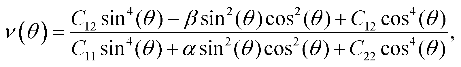
The band structure of 2H SnGe2N4 was computed using the PBE, PBE + SOC and HSE06 approaches along the symmetric Γ–M–K path of the 2H crystalline phase. The results are shown in Fig. 3, where the maximum of the valence band has been relocated to the Fermi level. The high discrepancy in band gap values, as seen in Table 1, is due to different calculating methods. Due to the loose treatment of the correlative effect, the underestimating of the band gap is a well-known issue of the GGA (PBE) method.38 PBE calculations yield a band gap of 0.934 eV for 2H SnGe2N4. The SOC parameter was included in the PBE + SOC calculations to account for the spin–orbit coupling effect.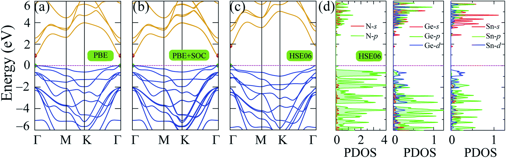 | ||
| Fig. 3 Band structure of 2H SnGe2N4 obtained by (a) PBE, (b) PBE + SOC and (c) HSE06 methods; (d) partial density of states of SnGe2N4 calculated by HSE06 method. | ||
The band gap calculated by PBE + SOC almost does not change, as shown in Fig. 3(b), because the quantum number L of p-block elements (Sn, Ge, and N) is not significant in comparison to f-block elements, where the relativistic influence is considerably stronger. However, there is still some interaction between the electrostatic field of the positively charged nucleus and the magnetic dipole of the electron, resulting in a higher density of lower valence bands, as illustrated in Fig. 3(b) and observed by PBE + SOC calculations. Aside from the SOC effect, the interaction of strongly correlated electrons from the d-orbitals of Sn and Ge atoms, as calculated using the HSE06 method,42 must also be considered. As a result, the over-delocalization of valence bands induced by the PBE method60 is reduced, resulting in a greater gap between the conduction and valence bands. As seen in Fig. 3(c), the HSE06 band gap has increased to about double that of the PBE band gaps. The weighted band structures in Fig. 4 show the considerable influence of the d-orbital interaction on the band structure of SnGe2N4.
 | ||
| Fig. 4 (a) Weighted band structures and (b) isosurfaces of the VBM and CBM charge densities of 2H SnGe2N4. | ||
As shown in Fig. 3(d) and 4, the valence band maxima (VBM) are primarily made up of d-orbitals of Sn and Ge atoms. As a result, changes in these bands have a considerable impact on the whole system’s band gap. Furthermore, this impact is extended to lower valence bands via substantial hybridization of N-p, Sn-d, and Ge-d orbitals, resulting in valence band extension compared to the PBE band structures. Meanwhile, the conduction band minima (CBM) are mainly constructed by the s-orbitals of Sn, Ge, and N atoms, and minor contribution from the p-orbitals of N atoms. The 1.8 eV band gap of 2H SnGe2N4 is larger than the ones, which were calculated by the PBE approach, of other MoSi2N4 monolayers, such as CrGe2N4, MoGe2N4 and WGe2N4, which are in the range of 1.27–1.51 eV.23 The 2H SnGe2N4, on the other hand, can absorb more visible and infrared light than MoSi2N4 and WSi2N4 monolayers (HSE band gaps are 2.23–2.57 eV).23
5 Photoelectric properties and charge carrier mobility of 2H SnGe2N4
The band structure of 2H SnGe2N4, calculated by the HSE06 approach, is characterized by an appropriate band gap for absorbing infrared and visible wavelengths, which constitute the majority of solar energy. Furthermore, the lowest conduction bands are very concave downward, as shown in Fig. 4, indicating high electron mobility. The mobility of holes, on the other hand, is expected to be low due to the relatively flat valence bands. As a result, 2H SnGe2N4 is predicted to be a good photoelectric material whose optical properties should be investigated. The light absorption ability of 2H SnGe2N4 is investigated using the absorption rate α(ω), which was computed using the dielectric function ε(ω) matrix values61 and is shown in Fig. 5. The imaginary part of the dielectric function was calculated by applying the Bethe–Salpeter equation (BSE) on top of the G0W0 method,62,63 which takes into consideration the interactions between electrons and between electrons and holes. The imaginary part of the dielectric function Im(ε) arises from the transition of electrons from occupied bands to unoccupied bands when stimulated by photons of appropriate energy, as seen in Fig. 3(d). As a result, the spectrum of Im(ε) is comparable to the spectrum of α(ω). | ||
| Fig. 5 (a) Imaginary dielectric constant ε and (b) absorption rate as a function of frequency ω. | ||
The absorption rate of 2H SnGe2N4 in the ultraviolet region is around 105 cm−1, with the highest peak near 4 eV. According to Fig. 3(d), this peak corresponds to the electron transition from the highest valence bands near −1 eV, which are dominated by N-p, Ge-d, and Sn-d orbitals, to the lowest conduction bands near 2 eV and 3 eV, which are dominated by N-p/s, Ge-s, and Sn-s orbitals. The absorption rate α(ω) reaches its maximum peaks in the visible range at 1.96 eV and 2.68 eV, with intensities of around 104. These peaks are caused by electron transitions from N-p orbitals in the valence bands to N-s/p, Ge-s, and Sn-s orbitals in the conduction bands. In general, the layered SnGe2N4 shares some common optical characteristics with 2H WGe2N4, WSi2N4, MoGe2N4, SnSi2N4 and MoSi2N4,23,36 where the absorption rate is as high as around 104 in the infrared and visible ranges, and it increases to 105 at higher energy levels of the ultraviolet range.
The charge carrier mobility was calculated by applying the deformation potential theory.64,65 For the 2D structures, the charge carrier mobility is denoted as μ2D and the elastic modulus as C2D. The value of μ2D is expressed via C2D, effective mass m* and the deformation energy constant Ed (defined based on Fig. 6(b)) as follows:
 | (3) |
where
 | (4) |
 | (5) |
 | (6) |
The formulas (3)–(6) use the reduced Planck constant ℏ, elementary charge e, unit cell volume Ω and the Boltzmann constant kB. The total energy E and uniaxial strain εuni were taken from energy–strain graph in Fig. 6(a).
 | ||
| Fig. 6 Dependence of (a) total energy and (b) band edge alignment on x and y uniaxial strains. | ||
The calculated transport parameters of 2H SnGe2N4 in Table 2 demonstrate the direction-independent effective masses of both holes and electrons, which can be explained by the isotropy of 2H SnGe2N4’s hexagonal honeycomb structure. Formula (4) illustrates an inverse relationship between effective mass and the differentiation of band edge curves. As a result, the electron’s low effective mass (−1.69m0) agrees well with the very concave conduction bands in Fig. 3. The increased effective mass of a hole, on the other hand, is the result of flat valence bands. As a result, the mobility of the electrons is substantially greater than that of the holes. These findings contradict those of 2D MoSi2N4, where the hole mobility is greater than the electron mobility21 due to more concave valence bands than conduction bands.66 The mobility of charge carriers in the x and y directions is approximately the same as in the SnSi2N4 compound.36 The 2H SnGe2N4’s electron mobility of 1061.66 cm2 V−1 s−1 is much higher the one of MoS2.67 In comparison with MX2N4 monolayers (M = Mo, W; X = Si, Ge),23 whose electron mobilities are in the range of 200–690 cm2 V−1 s−1 and hole mobilities are in the range of 1100–2490 cm2 V−1 s−1, the layered SnGe2N4 possesses higher electron mobility and lower hole mobility, which are about 1061.66 cm2 V−1 s−1 and 28.35 cm2 V−1 s−1, respectively.
| C2D (N m−1) | m* (m0) | Ed (eV) | μ2D (cm2 V−1 s−1) | ||
|---|---|---|---|---|---|
| Electron | x | 205.85 | 0.16 | −12.62 | 1061.66 |
| y | 202.45 | 0.16 | −12.62 | 1044.08 | |
| Hole | x | 205.85 | −1.69 | −6.84 | 28.35 |
| y | 202.45 | −1.69 | −6.99 | 26.69 | |
6 Effect of strain and external electric fields on the electronic structure of 2H SnGe2N4
Strain is well known to effectively modify the band structures of many 2D materials68,69 due to the fact that the Hamiltonian function of the 2D structure is greatly affected by the decrease of its symmetry.70 As shown in Fig. 3, the HSE06 band gap is larger than the PBE band gap, however both band structures share very similar patterns. The PBE method describes the electronic structures well with low computational cost. Therefore, the PBE methods are suitable for investigating the band gap variation of 2H SnGe2N4 due to strain and external electric field; the results are presented in Fig. 7, where the applied strain ranges from −10% to 10%, and the external electric field varies from −0.5 to 0.5 V Å−1. | ||
| Fig. 7 The effect of (a) biaxial strain and (b) an external electric field on the band gap of 2H SnGe2N4. | ||
The band gap of 2H SnGe2N4 grows almost linearly as the compressive strain reaches −10%, whereas tensile strain causes the band gap to decrease at the same slope down to zero at a strain of 7%. It is necessary to note that the PBE method underestimates the band gap values;71,72 the difference in band gap values obtained by PBE and HSE06, as shown in Table 1, is about 0.9 eV. However, the rates of decrease of the band gap, shown in Fig. 7, are about 0.1 eV every 1% of tensile strain and 0.25 eV every 0.1 V Å−1. Therefore, it is expected that the layered SnGe2N4 semiconductor will change into a metal under a higher rate of tensile strain or higher electric strength. External electric fields, both negative and positive, cause a decrease in the band gap of 2H SnGe2N4. The external electric fields cause the reduction of SnGe2N4’s band gap, as shown in Fig. 7(b) as a quadratic function of the electric strength. The variation of the band structure was estimated and is shown in Fig. 8 and 9 to obtain some insight into the behavior of the band gap of 2H SnGe2N4 under external variables.
 | ||
| Fig. 8 Band structure variation of 2H SnGe2N4 under biaxial strain ε(b). | ||
 | ||
| Fig. 9 Band structure variation of 2H SnGe2N4 under an external electric field E. | ||
As seen in Fig. 8, compressive strain primarily impacts the highest valence bands located at −2 to 0 eV. These valence bands are generated via the hybridization of s- and p-orbitals from N atoms and d-orbitals from Ge and Sn atoms, as seen in Fig. 4. According to the perturbation theory,73 the p- and d-states repel each other, and the interaction of d-states from neighboring atoms is similarly repulsive.74,75 Because the three atoms Sn, Ge and N come closer to each other under compressive pressures, the higher valence bands tend to be forced down, as illustrated in Fig. 8, resulting in a wider band gap of 2H SnGe2N4. Tensile strains have the opposite effect, causing the repulsion between orbitals to decrease, resulting in orbital overlap and narrowing the band gap.
The effect of external electric fields on the band gap of 2H SnGe2N4, as depicted in Fig. 9, originates from another mechanism where there is not structural deformation and the crystal field theory (CFT)76,77 plays an important role. The static external electric fields will mostly break the degeneracy of d and f orbitals. In the case of 2H SnGe2N4, the d orbitals from Ge and Sn atoms contribute a significant part to the highest valence bands. Therefore, when the degeneracy of these states is lifted by electric fields, the valence bands become flatter. As a result, the band gap of 2H SnGe2N4 is effectively and uniquely reduced by electric fields regardless of their sign.
In general, both strain and external electric field have notable effects on the band gap value of 2H SnGe2N4. Based on the fast and steady decrease of SnGe2N4’s band gap under tensile strains and external electric fields, a semiconductor–metal transition is expected to happen for layered SnGe2N4. In particular, tensile strains from 4–6% change the band gap nature from direct into indirect.
7 Conclusion
For the first time, the particular properties of layered SnGe2N4 were investigated using the PBE, PBE + SOC, and HSE06 methods. The layered SnGe2N4 was theoretically predicted to crystallize in a hexagonal structure with the space group Pm2. The present compound’s dynamic and thermal stabilities were confirmed using phonon dispersion estimates and AIMD modeling, respectively. Furthermore, 2H SnGe2N4 is mechanically stable, with the Young’s modulus (335.493 N m−1) and Poisson’s ratio (0.286) indicating that it is tougher than other layered materials in the same structural group, such as MoSi2N4, WSi2N4, and MoSi2N4.
The layered SnGe2N4 has a direct band gap of around 1.89 eV and highly concave downward conduction bands that are mostly made up of s-orbitals of the three elements. The fact that the highest valence bands are mostly produced by the hybridization of d-orbitals from Ge, Sn, and N atoms plays a significant role in the electrical, optical, and transport capabilities. The narrow band gaps and many peaks in the valence and conduction bands of 2H SnGe2N4 allow it to absorb light strongly in the infrared, visible, and even ultraviolet regions. This advantage, together with the extremely high electron mobility and a work function of roughly 6 eV, makes 2H SnGe2N4 a very promising photoelectric material. Because of its unique electronic structure, 2H SnGe2N4 actively responds to strain and external electric fields, leading to a noticeable change in the band gap values, and a possible transition between the semiconductor and metallic natures of layered SnGe2N4.
Conflicts of interest
There are no conflicts to declare.References
- L. Cheng, C. Zhang and Y. Liu, J. Am. Chem. Soc., 2019, 141, 16296–16302 CrossRef CAS PubMed.
- Y. Guo, K. Xu, C. Wu, J. Zhao and Y. Xie, Chem. Soc. Rev., 2015, 44, 637–646 RSC.
- A. Gupta, T. Sakthivel and S. Seal, Prog. Mater. Sci., 2015, 73, 44–126 CrossRef CAS.
- E. Pomerantseva and Y. Gogotsi, Nat. Energy, 2017, 2, 17089 CrossRef CAS.
- H. Song, J. Liu, B. Liu, J. Wu, H.-M. Cheng and F. Kang, Joule, 2018, 2, 442–463 CrossRef CAS.
- M. D. Stoller, S. Park, Y. Zhu, J. An and R. S. Ruoff, Nano Lett., 2008, 8, 3498–3502 CrossRef CAS PubMed.
- H. Zhang, ACS Nano, 2015, 9, 9451–9469 CrossRef CAS PubMed.
- Y. Zhang, Y.-W. Tan, H. L. Stormer and P. Kim, Nature, 2005, 438, 201–204 CrossRef CAS PubMed.
- Q. Fang, X. Zhao, Y. Huang, K. Xu, T. Min, P. K. Chu and F. Ma, J. Mater. Chem. C, 2018, 6, 4523–4530 RSC.
- W. Hu, L. Lin, R. Zhang, C. Yang and J. Yang, J. Am. Chem. Soc., 2017, 139, 15429–15436 CrossRef CAS PubMed.
- C. Huang, C. Chen, M. Zhang, L. Lin, X. Ye, S. Lin, M. Antonietti and X. Wang, Nat. Commun., 2015, 6, 7698 CrossRef PubMed.
- L. Ju, J. Shang, X. Tang and L. Kou, J. Am. Chem. Soc., 2020, 142, 1492–1500 CrossRef CAS PubMed.
- M. Qiao, J. Liu, Y. Wang, Y. Li and Z. Chen, J. Am. Chem. Soc., 2018, 140, 12256–12262 CrossRef CAS PubMed.
- Y. Wan, L. Wang, H. Xu, X. Wu and J. Yang, J. Am. Chem. Soc., 2020, 142, 4508–4516 CrossRef CAS PubMed.
- A. Daus, S. Vaziri, V. Chen, c. Köroğlu, R. W. Grady, C. S. Bailey, H. R. Lee, K. Schauble, K. Brenner and E. Pop, Nat. Electron., 2021, 4, 495–501 CrossRef CAS.
- L. Maggini and R. R. Ferreira, J. Mater. Chem. C, 2021, 9, 15721–15734 RSC.
- S. B. Mitta, M. S. Choi, A. Nipane, F. Ali, C. Kim, J. T. Teherani, J. Hone and W. J. Yoo, 2D Mater., 2021, 8, 012002 CrossRef CAS.
- N. Mounet, M. Gibertini, P. Schwaller, D. Campi, A. Merkys, A. Marrazzo, T. Sohier, I. E. Castelli, A. Cepellotti, G. Pizzi and N. Marzari, Nat. Nanotechnol., 2018, 13, 246–252 CrossRef CAS PubMed.
- T. Roy, M. Tosun, J. S. Kang, A. B. Sachid, S. B. Desai, M. Hettick, C. C. Hu and A. Javey, ACS Nano, 2014, 8, 6259–6264 CrossRef CAS PubMed.
- X. Zhang, L. Hou, A. Ciesielski and P. Samorì, Adv. Energy Mater., 2016, 6, 1600671 CrossRef.
- Y.-L. Hong, Z. Liu, L. Wang, T. Zhou, W. Ma, C. Xu, S. Feng, L. Chen, M.-L. Chen, D.-M. Sun, X.-Q. Chen, H.-M. Cheng and W. Ren, Science, 2020, 369, 670–674 CrossRef CAS PubMed.
- K. S. Novoselov, Natl. Sci. Rev., 2020, 7, 1842–1844 CrossRef PubMed.
- B. Mortazavi, B. Javvaji, F. Shojaei, T. Rabczuk, A. V. Shapeev and X. Zhuang, Nano Energy, 2021, 82, 105716 CrossRef CAS.
- S.-D. Guo, W.-Q. Mu, Y.-T. Zhu and X.-Q. Chen, Phys. Chem. Chem. Phys., 2020, 22, 28359–28364 RSC.
- H. Yao, C. Zhang, Q. Wang, J. Li, Y. Yu, F. Xu, B. Wang and Y. Wei, Nanomaterials, 2021, 11, 559 CrossRef CAS PubMed.
- B. Mortazavi, F. Shojaei, B. Javvaji, T. Rabczuk and X. Zhuang, Mater. Today Energy, 2021, 22, 100839 CrossRef CAS.
- H. Zhong, W. Xiong, P. Lv, J. Yu and S. Yuan, Phys. Rev. B, 2021, 103, 085124 CrossRef CAS.
- B. Anam and N. Gaston, J. Phys.: Condens. Matter, 2021, 33, 125901 CrossRef PubMed.
- B. v. d. Broek, M. Houssa, E. Scalise, G. Pourtois, V. V. Afanas’ev and A. Stesmans, 2D Mater., 2014, 1, 021004 CrossRef.
- J. Ouyang, L. Zhang, L. Li, W. Chen, Z. Tang, X. Ji, C. Feng, N. Tao, N. Kong, T. Chen, Y.-N. Liu and W. Tao, Nano-Micro Lett., 2021, 13, 90 CrossRef CAS PubMed.
- F.-f. Zhu, W.-j. Chen, Y. Xu, C.-l. Gao, D.-d. Guan, C.-h. Liu, D. Qian, S.-C. Zhang and J.-f. Jia, Nat. Mater., 2015, 14, 1020–1025 CrossRef CAS PubMed.
- X. Chen, R. Meng, J. Jiang, Q. Liang, Q. Yang, C. Tan, X. Sun, S. Zhang and T. Ren, Phys. Chem. Chem. Phys., 2016, 18, 16302–16309 RSC.
- A. I. Khan, T. Chakraborty, N. Acharjee and S. Subrina, Sci. Rep., 2017, 7, 16347 CrossRef PubMed.
- Y. Yin, M. Yi and W. Guo, ACS Appl. Mater. Interfaces, 2021, 13, 45907–45915 CrossRef CAS PubMed.
- S.-D. Guo, Y.-T. Zhu, W.-Q. Mu, L. Wang and X.-Q. Chen, Comput. Mater. Sci., 2021, 188, 110223 CrossRef CAS.
- M. Tian, C. Wei, J. Zhang, J. Wang and R. Yang, Phys. Rev. B, 2021, 103, 195305 CrossRef CAS.
- C. Shen, L. Wang, D. Wei, Y. Zhang, G. Qin, X.-Q. Chen and H. Zhang, Phys. Chem. Chem. Phys., 2022, 24, 3086–3093 RSC.
- J. P. Perdew, K. Burke and M. Ernzerhof, Phys. Rev. Lett., 1996, 77, 3865–3868 CrossRef CAS PubMed.
- G. Kresse and J. Furthmüller, Phys. Rev. B: Condens. Matter Mater. Phys., 1996, 54, 11169–11186 CrossRef CAS PubMed.
- S. Grimme, J. Antony, S. Ehrlich and H. Krieg, J. Chem. Phys., 2010, 132, 154104 CrossRef PubMed.
- P. E. Blöchl, Phys. Rev. B: Condens. Matter Mater. Phys., 1994, 50, 17953–17979 CrossRef PubMed.
- J. Heyd, G. E. Scuseria and M. Ernzerhof, J. Chem. Phys., 2003, 118, 8207–8215 CrossRef CAS.
- A. Togo and I. Tanaka, Scr. Mater., 2015, 108, 1–5 CrossRef CAS.
- Y. An, K. Wang, S. Gong, Y. Hou, C. Ma, M. Zhu, C. Zhao, T. Wang, S. Ma, H. Wang, R. Wu and W. Liu, npj Comput. Mater., 2021, 7, 45 CrossRef CAS.
- L. Wang, Y. Shi, M. Liu, A. Zhang, Y.-L. Hong, R. Li, Q. Gao, M. Chen, W. Ren, H.-M. Cheng, Y. Li and X.-Q. Chen, Nat. Commun., 2021, 12, 2361 CrossRef CAS PubMed.
- W.-Y. Ching, S.-D. Mo, L. Ouyang, P. Rulis, I. Tanaka and M. Yoshiya, J. Am. Ceram. Soc., 2002, 85, 75–80 CrossRef CAS.
- T. J. Giese and D. M. York, J. Chem. Phys., 2010, 133, 244107 CrossRef PubMed.
- W. Kaim, Angew. Chem., Int. Ed. Engl., 1989, 28, 1073–1074 CrossRef.
- K. H. Michel and B. Verberck, Phys. Rev. B, 2009, 80, 224301 CrossRef.
- A. Bafekry, M. Faraji, D. M. Hoat, M. Shahrokhi, M. M. Fadlallah, F. Shojaei, S. A. H. Feghhi, M. Ghergherehchi and D. Gogova, J. Phys. D: Appl. Phys., 2021, 54, 155303 CrossRef CAS.
- T. V. Vu, C. V. Nguyen, H. V. Phuc, A. A. Lavrentyev, O. Y. Khyzhun, N. V. Hieu, M. M. Obeid, D. P. Rai, H. D. Tong and N. N. Hieu, Phys. Rev. B, 2021, 103, 085422 CrossRef CAS.
- N. N. Hieu, H. V. Phuc, A. I. Kartamyshev and T. V. Vu, Phys. Rev. B, 2022, 105, 075402 CrossRef CAS.
- T. V. Vu and N. N. Hieu, J. Phys.: Condens. Matter, 2022, 34, 115601 CrossRef CAS PubMed.
- C. Kittel, Introduction to Solid State Physics, 7th edn, John Wiley & Sons, 1996 Search PubMed.
- T. Shimada, F. S. Ohuchi and B. A. Parkinson, Jpn. J. Appl. Phys., 1994, 33, 2696–2698 CrossRef CAS.
- N. Bhalla, S. Taneja, P. Thakur, P. K. Sharma, D. Mariotti, C. Maddi, O. Ivanova, D. Petrov, A. Sukhachev, I. S. Edelman and A. Thakur, Nano Lett., 2021, 21, 9780–9788 CrossRef CAS PubMed.
- Z. Yu, W. Feng, W. Lu, B. Li, H. Yao, K. Zeng and J. Ouyang, J. Mater. Chem. A, 2019, 7, 11160–11169 RSC.
- S. Kouser, A. Thannikoth, U. Gupta, U. V. Waghmare and C. N. R. Rao, Small, 2015, 11, 4723–4730 CrossRef CAS PubMed.
- D. Singh, S. K. Gupta, Y. Sonvane, A. Kumar and R. Ahuja, Catal. Sci. Technol., 2016, 6, 6605–6614 RSC.
- H. J. Kulik, J. Chem. Phys., 2015, 142, 240901 CrossRef PubMed.
- M. O’Donnell, E. T. Jaynes and J. G. Miller, J. Acoust. Soc. Am., 1981, 69, 696–701 CrossRef.
- M. Shishkin and G. Kresse, Phys. Rev. B: Condens. Matter Mater. Phys., 2006, 74, 035101 CrossRef.
- F. Karlický and M. Otyepka, J. Chem. Theory Comput., 2013, 9, 4155 CrossRef PubMed.
- S. Bruzzone and G. Fiori, Appl. Phys. Lett., 2011, 99, 222108 CrossRef.
- S. Poncé, W. Li, S. Reichardt and F. Giustino, Rep. Prog. Phys., 2020, 83, 036501 CrossRef PubMed.
- Q. Wu, L. Cao, Y. S. Ang and L. K. Ang, Appl. Phys. Lett., 2021, 118, 113102 CrossRef CAS.
- Y. Cai, G. Zhang and Y.-W. Zhang, J. Am. Chem. Soc., 2014, 136, 6269–6275 CrossRef CAS PubMed.
- A. Chaves, J. G. Azadani, H. Alsalman, D. R. da Costa, R. Frisenda, A. J. Chaves, S. H. Song, Y. D. Kim, D. He, J. Zhou, A. Castellanos-Gomez, F. M. Peeters, Z. Liu, C. L. Hinkle, S.-H. Oh, P. D. Ye, S. J. Koester, Y. H. Lee, P. Avouris, X. Wang and T. Low, npj 2D Mater. Appl., 2020, 4, 29 CrossRef CAS.
- E. F. Procopio, R. N. Pedrosa, F. A. L. de Souza, W. S. Paz and W. L. Scopel, Phys. Chem. Chem. Phys., 2020, 22, 3520–3526 RSC.
- X.-B. Xiao, Q. Ye, Z.-F. Liu, Q.-P. Wu, Y. Li and G.-P. Ai, Nanoscale Res. Lett., 2019, 14, 322 CrossRef PubMed.
- H. Xiao, J. Tahir-Kheli and W. A. Goddard, J. Phys. Chem. Lett., 2011, 2, 212–217 CrossRef CAS.
- J. P. Perdew, W. Yang, K. Burke, Z. Yang, E. K. U. Gross, M. Scheffler, G. E. Scuseria, T. M. Henderson, I. Y. Zhang, A. Ruzsinszky, H. Peng, J. Sun, E. Trushin and A. Görling, Proc. Natl. Acad. Sci. U. S. A., 2017, 114, 2801–2806 CrossRef CAS PubMed.
- H. D. Megaw, Acta Crystallogr., 1958, 11, 451–452 CrossRef.
- Q. Wan, J. Yang, W.-P. To and C.-M. Che, Proc. Natl. Acad. Sci. U. S. A., 2021, 118, e2019265118 CrossRef CAS PubMed.
- L. Wang, Y. Wen, Y. Ji, H. Cao, S. Li, S. He, H. Bai, G. Liu, L. Zhang, H. Bao, J. Wang, Y. Li, B. Zhang and H. Peng, J. Mater. Chem. A, 2019, 7, 14455–14461 RSC.
- H. Bethe, Ann. Phys., 1929, 395, 133–208 CrossRef.
- J. H. Van Vleck, Phys. Rev., 1932, 41, 208–215 CrossRef CAS.
| This journal is © The Royal Society of Chemistry 2022 |