
 Open Access Article
 This Open Access Article is licensed under a
 Creative Commons Attribution 3.0 Unported Licence
Band offset engineering at C2N/MSe2 (M = Mo, W) interfaces†
Amine Slassi *ab
*ab
aIstituto Nanoscienze-CNR, Via Campi 213a, I-41125 Modena, Italy. E-mail: a.slassi22@gmail.con; amine.slassi@nano.cnr.it
bLaboratory for Chemistry of Novel Materials, Université de Mons, Place du Parc 20, 7000 Mons, Belgium
First published on 20th April 2022
Abstract
Stacking layered two-dimensional materials in a type-II band alignment block has provided a high-performance method in photocatalytic water-splitting technology. The key parameters in such heterostructure configurations are the valence and conduction band offsets at the interface, which determine the device performance. Here, based on density functional theory calculations, the bandgap and band offsets at C2N/MSe2 (M = Mo, W) interfaces have been engineered. The main findings demonstrate that the C2N monolayer interacts with both MoSe2 and WSe2 monolayers through weak van der Waals interactions. These heterostructures possess a narrower indirect bandgap and a typical type-II heterostructure feature, being suitable for promoting the separation of photogenerated electron–hole pairs. The calculated Gibbs free energy of hydrogen adsorption demonstrates a reduction in the overpotential, towards the hydrogen evolution reaction, upon forming heterostructures. To further tune the bandgap values and band offsets of heterostructures, the external perturbations are included through a vertical strain and finite electric field. It is found that both the vertical strain and electric field strongly modulate the bandgap values and the magnitude of the band offsets, while the typical type-II band alignment remains preserved. It is noticeable that the band offset magnitudes of the C2N/MoSe2 and C2N/WSe2 heterostructures are more sensitive to an external electric field than to a vertical interlayer strain.
1 Introduction
Porous carbon nitride (C2N) has attracted tremendous interest as a metal-free two-dimensional (2D) semiconductor photocatalyst for hydrogen production from visible-light driven water splitting.1,2 This interest stems from its fascinating features such as an appropriate direct band gap value of 1.96 eV covering a considerable part of the visible-light absorption,3 high structural stability4 and suitable band edge positions.5 Several experimental studies demonstrated that 2D C2N can be an efficient photocatalyst in the hydrogen evolution reaction.1,2 However, similar to the g-C3N4 material, the fast recombination of photoinduced electron–hole pairs also prevents achieving a high photocatalyst performance of the C2N material.3A new paradigm in photocatalytic devices is to vertically stack 2D materials, with different ionization potentials and electronic affinities to generate a donor–acceptor heterostructure photocatalyst, which has demonstrated to be the most effective approaches for suppressing the electron–hole pairs recombination and improving the photocatalytic performance.2,6,7 Recently, several C2N-based vdW heterostructures such as C2N/MoS2, C2N/Janus monochalcogenides,8 C2N/aza-CMP,9 C2N/h-BN,10 C2N/cobalt-oxide,2 C2N/CdS,11 C2N/g-C3N4 (ref. 12) and C2N/WS2 (ref. 13) were studied. Unsurprisingly, the results demonstrated that a significant enhancement in the photocatalytic efficiency can be achieved in such vdW heterostructures as compared to the single-layered form. For instance, Mahmood et al.2 experimentally demonstrated that the stacking C2N with cobalt-oxide, in a heterostructure stack, results in higher catalytic activities for hydrogen (H2) production with a generation-rate comparable to that of the best reported values for catalysts containing precious noble metals.
Whatever, the band edge alignment of constituting components, with respect to each other, is a key parameter determining the heterostructure device performance.14,15 For photocatalytic applications, a heterostructure with a type-II band alignment configuration demonstrated to efficiency separate the photogenerated electron–hole pairs at the interface for highly efficient water reduction and oxidation.6,16 In such a type-II configuration, the magnitude of the conduction band offset (CBO; defined as the difference in the electron affinities of two constituting components) and valence band offset (VBO; the difference in the ionization potentials) determine the magnitude of the built-in electric at the interface that in turn separates the photogenerated electrons and holes in space. Koda et al. demonstrated, by the first principles calculations, that tailoring the band offsets (CBO and VBO) at phosphorene/TMDs strongly modulate the electronic properties of heterostructures.17 Zhang et al. showed that the band alignment engineering is a good approach to achieve a higher photocatalyst performance of MoS2/GaN heterostructure for hydrogen generation.18
In the present study, the electronic properties of C2N/MoSe2 and C2N/WSe2 heterostructures have been studied by employing the density functional theory (DFT). The band energy diagrams show a band alignment type II with large band offsets in the valence band maximums and conduction band minimums, which providing strong driving forces to pump the photo-generated electrons from MoSe2 (WSe2) layer to C2N layer, and the photo-generated holes in the opposite directions. The band offsets and band gap values have been further engineered by modulating the interlayer electronic interactions and applying external perturbations such as a interlayer strain and a finite electrical field.
2 Calculation methods
All calculations were performed by using the Vienna ab initio simulation package (VASP). The interaction ion-cores and valence-electrons were described by projected – augmented wave (PAW) method with a cutoff energy of 600 eV.19,20 GGA within Perdew, Burke, and Ernzerhof (PBE) approach was used for the exchange correlation functional.21 Due to the presence of the van der Waals (vdW) interactions in our studied heterostructures, the Grimme 2D was included.22 Monkhorst–Pack 2 × 2 × 1 and 5 × 5 × 1 k-point grids are used to sample the Brillouin zone (BZ) for geometry optimizations and the electronic structure calculations, respectively. All ions are allowed to be relaxed till their residual Hellmann–Feynman forces are less than 0.01 eV Å−1.The optical absorptions of C2N monolayer as well two MoSe2/C2N and WSe2/C2N heterostructures were calculated by the following formula:23
 | (1) |
3 Results and discussion
3.1 . Properties of heterostructures
The geometry relaxation of isolated C2N, MoSe2 and WSe2 monolayers was first considered. The lattice parameters for C2N, MoSe2 and WSe2 monolayers are calculated to be 3.32, 3.31 and 8.318 Å, respectively, which are in good agreement with the experimental and previous theoretical results.17,28,29 To construct the heterostructures, 5 × 5 × 1 unit cells of MoSe2 (WSe2) were placed on 2 × 2 × 1 unit cells of C2N resulting in a low lattice mismatch, less than 0.5% for both heterostructures, which implies that the effect of lattice mismatch on the electronic properties of individual monolayers remains unaffected in this study. The supercell heterostructures contain 147 atoms, including 72 C, 50 Se, and 25 Mo (W) atoms. The equilibrium geometries of MoSe2/C2N and MoSe2/C2N heterostructures are shown in Fig. 1. | ||
| Fig. 1 Top and side views of the optimized of (a) C2N/MoSe2 and (b) C2N/WSe2 heterostructures. d0 denotes the equilibrium interlayer distance. | ||
Upon heterostructure configurations, the C2N, MoSe2 and WSe2 monolayers keep their plane and hexagonal atomic network intact without any remarkable distortions. The calculated equilibrium interlayer distance between C2N and MoSe2 (WSe2) is 3.36 Å (3.32), close to the interlayer distance of 3.34 Å at C2N/MoS2 (ref. 7) and 3.33 Å WS2/C2N heterostructures.13 The corrugation of C2N is still less than 0.043 Å (0.065) in MoSe2/C2N (WSe2/C2N) heterostructure, which is smaller than the significant buckled height at C2N/g-C3N4 heterostructure.12
To quantitatively characterize the interlayer interactions, the binding energy (Eb) is estimated by following equation:
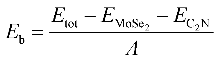 | (2) |
The electronic structures of MoSe2/C2N and WSe2/C2N heterostructures at equilibrium interlayer distance were analyzed. The obtained band structures are shown in Fig. 2, indicating that both C2N/MoSe2 and C2N/WSe2 heterostructures are semiconductors with indirect band gaps at G–K points and values of 0.8 eV and 0.58 eV, respectively, smaller than the direct band gaps of individual layers of 1.73 eV (C2N) at G-point, 1.56 eV (MoSe2) and 1.67 eV (WSe2) at k-point, due mainly to the band offsets at the band edges. Thus, the electrons can be easier photo-excited from the valence band (VB) to the conduction band (CB) in heterostructures under the IR and visible light radiations, which improves the electron–hole photo-generation rate as compared to the individual monolayers. Note that the bandgap values calculated at the PBE level are lower than the quasi-particle bandgap values found at the GW many-body theory level34 owing to the shortening of GGA in accurately describing the exchange–correlation (xc) functional. Notwithstanding, comparing at the GGA level the relative values of the bandgap of two different materials and the relative alignment of their valence or conduction band edges are still reasonable, which will not qualitatively affect the interpretation of band values based on my calculations.6 Indeed, the use of GW induces only a rigid band shift of VBM and CBM by the same amount but in the inverse directions with respect to the same band-gap-center by DFT-calculations.14,35
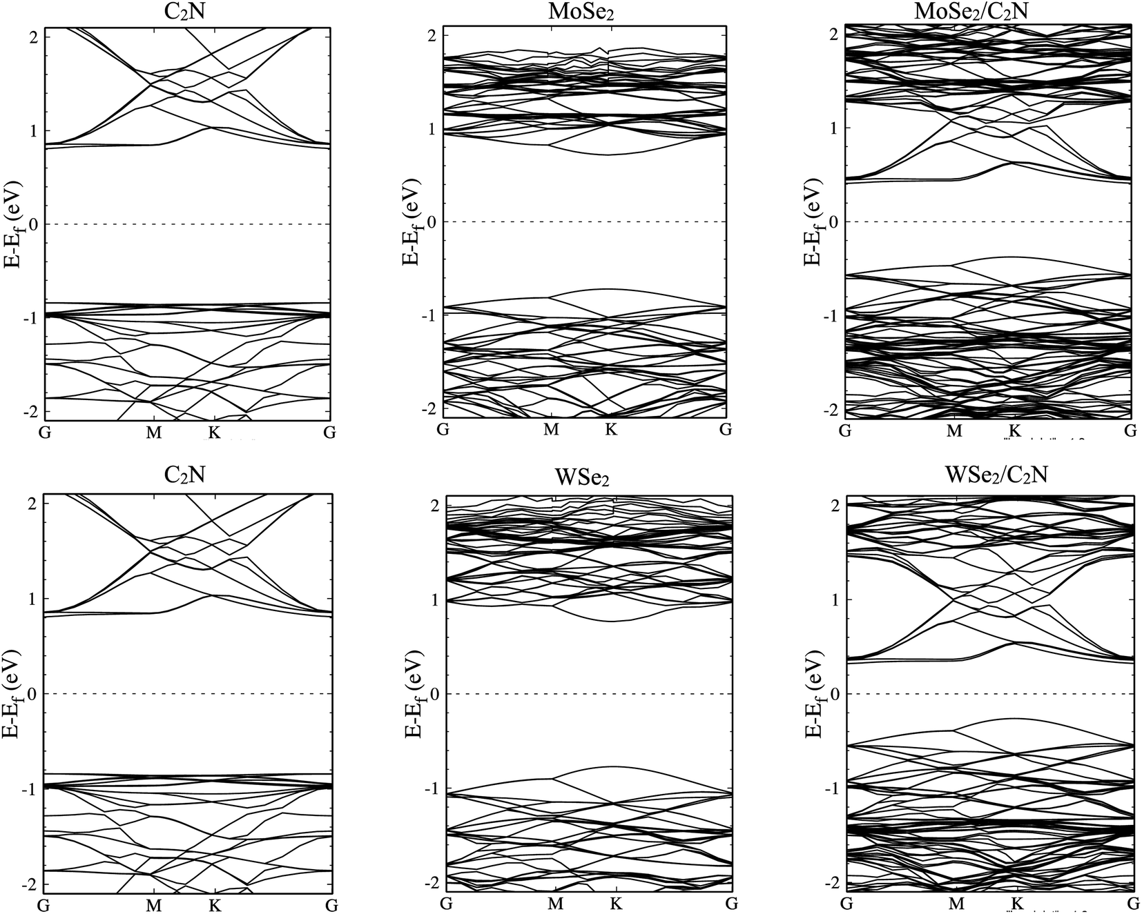 | ||
| Fig. 2 Band structures of isolated monolayers and their heterostructures. | ||
The calculated density of states, as shown in Fig. S1 (ESI†), show that the top part of the valence band is formed by states from MoSe2 (WSe2) and the bottom part of the conduction band is formed by states from C2N for both heterostructures. The deep orbital analysis shows that the valence band maximum (VBM) is dominated by Mo-dx2−y2 orbital (W-dx2−y2), while the conduction band minimum (CBM) is dominated by N-pz orbital contributions. On the other hand, no overlap of MoSe2 (WSe2) orbitals with those from C2N layer is observed at band edges.
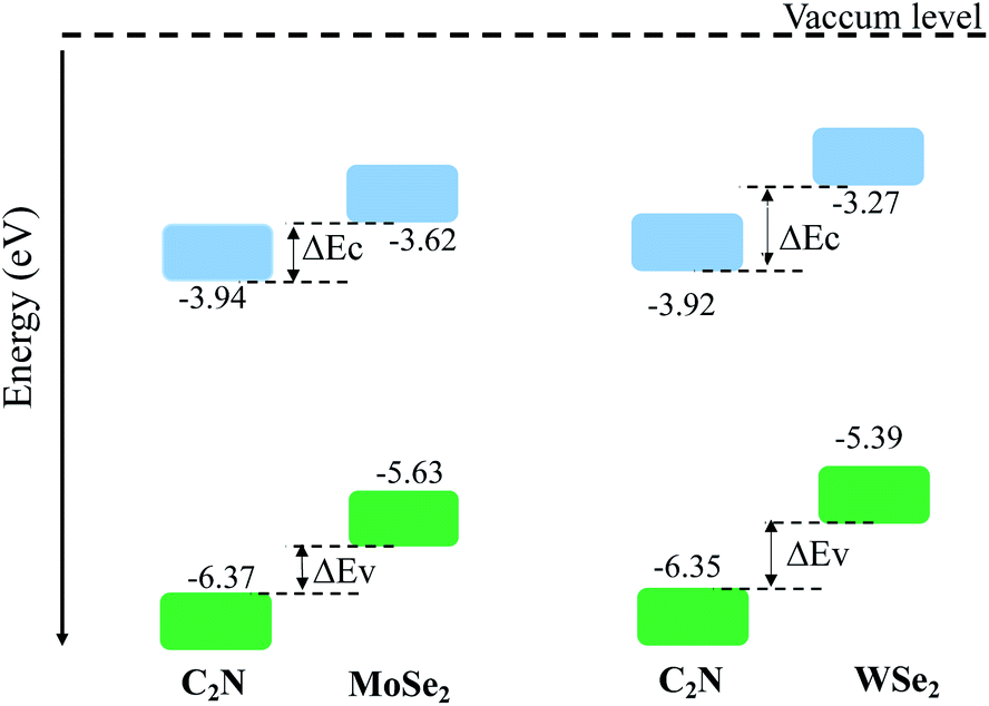
The calculated electronic band alignment diagrams of MoSe2/C2N and WSe2/C2N heterostructures, at equilibrium phases, are shown in Fig. 3, in which the zero is referenced to the vacuum level. It is found that the CBM and VBM of the C2N layer are lower in energy than those of MoSe2 (WSe2) layer, which indicates that the MoSe2/C2N heterostructure (WSe2/C2N) is expected to form a type II band alignment configuration. This would lead to a significant enhancement in the photocatalytic H2 generation.6 The calculated VBO and CBO between C2N and MoSe2 (WSe2) layers are ΔEv = 0.84 eV (1.05) and ΔEc = 0.65 eV (0.96) respectively. These values are larger than the CBO (0.54 eV) and VBO (0.67 eV) at WS2/C2N heterostructure.13 For the sake of comparison, I calculated the band alignment of heterostructures at HSE06 level, see Fig. S2.† Overall, the band alignment at HSE06 level shows similar type-II band alignment configuration, while the difference being only a small variation in the band offsets (CBO and VBO). This implies that although the GGA-PBE significantly underestimates the bandgap values of individual components, the main interpretation would not be qualitatively affected when one considers the engineering of the band offsets. To avoid the high computational cost at HSE06 level, I therefore focused on GGA-PBE for engineering the band offsets at heterostructures under different external perturbations.
 | ||
| Fig. 3 Band alignments of heterostructures at interactive configurations. | ||
On the other hand, these large band offsets would establish a strong built-in electrical field breaking the photo-generated electron–hole exciton bonds at the interface, which then drives the generated electrons and holes to the opposite special sides across the interface. Hence, under the light illumination, the electrons will be excited form the valence bands of both C2N and MoSe2 (WSe2) to their conduction bands, therefore, the photo-generated electrons in the conduction band of MoSe2 (WSe2) can be spontaneously transferred to the conduction band of C2N due to the generated strong electrical force. Meantime, the photo-generated holes in the valence band of C2N can be also spontaneously transferred to the valence band of MoSe2 (WSe2). This makes C2N a negatively charged layer and MoSe2 (WSe2) a positively charged layer, forming a n–p heterojunction. Therefore, such an interfacial charge separation enhances the electron–hole photo-generations by suppressing their recombination.
Sequentially, I estimated the charge transferred between C2N and MoSe2 (WSe2) layer by using the Bader charge analysis. The amount of electron transferred from MoSe2 (WSe2) to C2N is estimated to be 0.18 |e| (0.20 |e|) per supercell. These results are in good trend with what predicted from the band alignment diagrams. Moreover, the electron transfer across interface leads to a formation of an interfacial dipole layer and an accompanying potential step ΔV due to bending band as shown in Fig. S3 (ESI†). The ΔV step is defined as the difference between the right and left values of the potential profile with respect of the interface, which is considered as a barrier height of the carrier injections in heterojunction (see Fig. S3 in ESI†). Indeed, the formation of bending band in the heterostructures is suitable for charge separation. The calculated values of ΔV are 0.13 eV and 0.12 eV for C2N/MoSe2 and C2N/WSe2, respectively.
To further explore the combined effects of C2N and MoSe2 (WSe2), I investigated the optical properties of the isolated C2N monolayer as well as the MoSe2/C2N and WSe2/C2N heterostructures. The absorption spectra along two main polarization vectors, parallel (α∥) and normal (α⊥) to the C2N plane are shown in Fig. 4. From the first view, the optical absorption strength of isolated C2N along parallel polarization (α∥) is higher than that along the normal (α⊥) polarization vector within the IR and visible light ranges. The absorption threshold for isolated C2N monolayer is lied at the photon energy of 1.67 eV, which is close to bandgap energy. This is due mainly to electron transitions from VBM to CBM; while the other peaks lying above this threshold are mainly originated from the different inter-band electron transitions from VB to CB of isolated C2N monolayer.
 | ||
| Fig. 4 Calculated absorption spectra for C2N, MoSe2/C2N and WSe2/C2N along: (a) parallel (α∥) and (b) normal (α⊥) direction of the C2N monolayer plane, respectively. The dashed lines denote the visible light range. | ||
Upon heterostructure configurations, the optical absorption strength over the visible light range is significantly enhanced for both MoSe2/C2N and WSe2/C2N heterostructures with a red-shift in the absorption threshold towards low energy photons, which is an extra value for C2N based photocatalyst. This red shift of the absorption edge is mainly due to effect of interfacial interactions and reduced band gap values upon heterostructure configuration, the photogenerated electrons would be directly excited from the VBM of MoSe2 (WSe2) to the CBM of C2N component. For the sake of comparison, the enhancement of optical absorption is obviously higher at WSe2/C2N than that at MoSe2/C2N heterostructure; this is rationalized by the fact that the magnitude of band offsets at WSe2/C2N is larger.
3.2. Hydrogen evolution reaction
In order to assess the effect of the interface formation on the hydrogen evolution reaction (HER) efficiency, the Gibbs free energy diagram of hydrogen adsorption (ΔGH*) was quantified. More detailed information is found in the ESI.† Previous studies demonstrated that the Gibbs free energy of hydrogen adsorption (ΔGH) is the reasonable descriptor of HER activity.36 Of note, the value of (ΔGH*) close to zero results in a fast hydrogen release step and therefore suitable material for HER. The lower value of (ΔGH*) indicated strong bonds with H atoms, resulting in a slow hydrogen evolution process. For the sake of completeness, I also considered a single Pt atom anchored on the C2N surface. Here, the energetic calculation tests of Pt-adsorption over different sites indicated that Pt atom prefers to be anchored on the cavity site of C2N forming bonds with N atoms, which is similar to previous calculations.37 On the other hand, the hydrogen atom in the pristine monolayer/heterostructure prefers to chemically bind on top of N sites, indicating that the N atom sites are the active sites for HER reaction. For the Pt-anchored on C2N, the Pt atom sites are found to be active sites. Thus, the diagram of free energy for the hydrogen adsorption (ΔGH*) is computed as shown in Fig. 5. The value of ΔGH* for the isolated C2N sheet is calculated to be −0.91 eV, which indicates a strong chemical bond between H and N atoms. This would require an overpotential of +0.91 eV for an overall H2 evolution. Upon heterostructure configuration, the value of (ΔGH*) decreases by 18 and 11 meV for MoSe2/C2N and WSe2/C2N, respectively. This is rationalized by the fact that the charge transfer from MoSe2 (WSe2) sheet to C2N modifies the charge density over the active sites, which in turn balance the photocatalytic activity towards the HER. Thus, the controlling of the band alignment and charge transfer across the interface would optimize the catalytic efficiency of C2N-based heterostructures. It should be interesting to note that the anchoring of a single Pt atom on C2N surface significantly decreases the overpotential toward HER, while the values of (ΔGH*) further decrease upon heterostructure configurations. | ||
| Fig. 5 Calculated ΔGH* diagram for: (a) pristine and (b) Pt anchored on isolated C2N surface. The top view of H adsorbed on pristine and Pt anchored on C2N are inserted on (a) and (b), respectively. | ||
3.3. Applying a vertical strain
The electronic properties of 2D heterostructures can be modulated by artificially varying the interlayer distance. By varying the vdW interlayer spacing in the heterostructures, it is possible to change the binding energy, bandgap values and charge transfer between the constituents of the hetero-structure due to the alteration in the interlayer electronic coupling. Such a vertical strain has been proven to be an effective approach to alter the electronic structures of heterostructures in many theoretical studies.38–40 In the experimental point of view, the applied vertical strain to vdW hetero-structures can be applicable by employing the diamond anvil cells.41 In our calculations, the strain was applied by varying the interlayer distance by −0.3, 0.3, 0.6, 0.9 and 1.2 Å with respect of equilibrium distance (d0). The evolutions of binding energy, bandgap and Bader charge transfer values at heterostructures as a function of the applied vertical strain are shown in Fig. 6. | ||
| Fig. 6 Variation as a function of interlayer distance of: (a) binding energy, (b) bandgap energy and (c) Bader charge transfer. Red curve for C2N/MoSe2 and black curve for C2N/WSe2 heterostructures. Zero of the interlayer distance scale is put at the equilibrium position. | ||
Here, when both tensile and compressive strain are applied, the binding energy is slightly decreased, as shown in Fig. 6-a, which implies that the thermodynamic stability is slightly perturbated by such a moderate applied vertical strain.
The evolution of the band gap value as a function of the applied strain is shown in Fig. 6-b. The bandgap is still indirect regardless the tensile/compressive applied strain. Upon applying a compressive vertical strain, the band gap decreases due mainly to enhancement in the interaction between the orbital pz of C2N layer and orbital dx2−y2 of MoSe2 (WSe2) layer. Therefore, the edge absorption would be red-shifted resulting in an enhanced optical absorption over the IR and visible regions. In contrast, applying a tensile vertical strain leads to an increase in the bandgap value which must be due to suppressing of interaction between C2N monolayer and MoSe2 (WSe2) monolayer. In this last case, the absorption edge would be blue-shifted.
The modification in the interaction between C2N and MoSe2 (WSe2) is also associated to the charge transfer across the interface. The Bader charge transferred from the MoSe2 (WSe2) layer to C2N layer as a function of the vertical strain is also calculated, as shown in Fig. 5-c. At equilibrium interlayer distance, the charge transferred is calculated to be 0.18 |e| (0.20 |e|). Upon the interlayer distance decreases, the charge transfer considerably increases. Whereas, the charge transfer decreases as the interlayer increases. This demonstrates a strong dependence of the charge transfer on the vertical strain and significant modulation of interlayer electronic process and the band alignment at interface.
The effect of the vertical strain on the band offset is shown in Fig. 7. Interestingly, the band alignment type II is still preserved upon applying a tensile/compressive strain. The increasing in the interlayer distance results in a decrease of both VBO and CBO of heterostructures due to weakening in the interlayer interaction.
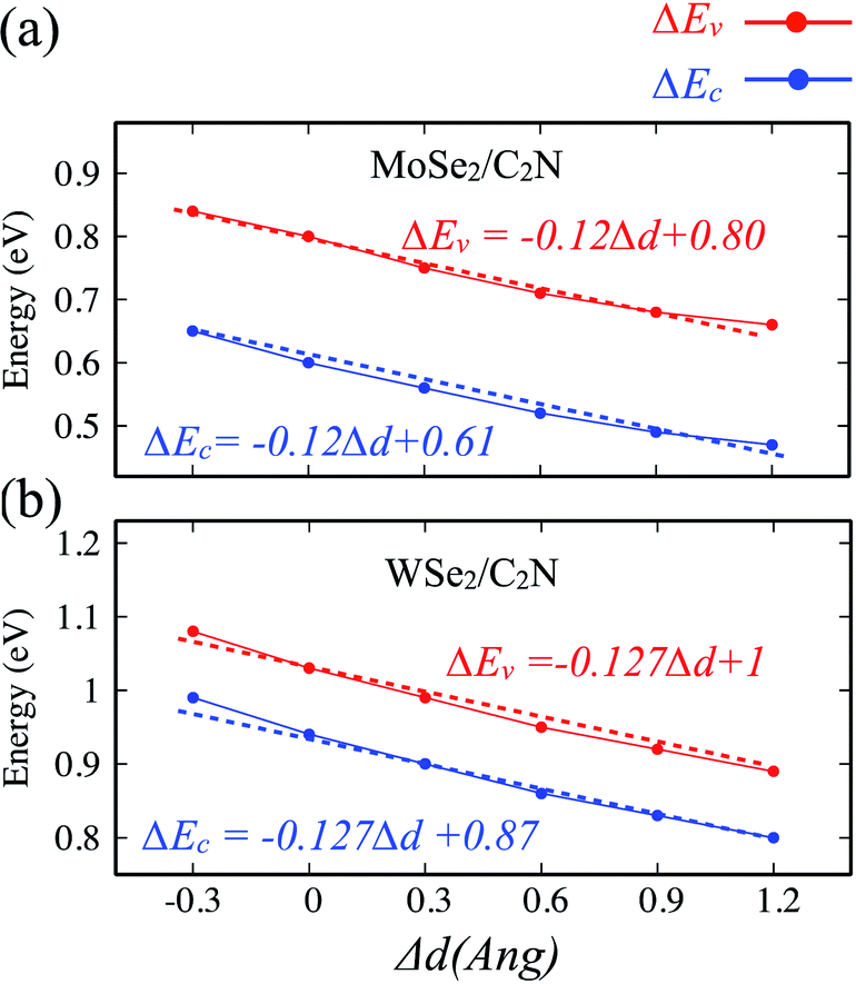 | ||
| Fig. 7 Variation of band offsets ΔEc/ΔEv as a function of the vertical strain for (a) MoSe2/C2N and (b) WSe2/C2N heterostructures. | ||
By placing the layers very far each other, the VBO and CBO trend towards those of isolated systems. In contrast, the decreasing in the interlayer distance leads to increasing in VBO and CBO due to increasing in the interlayer electronic interaction and orbital overlapping.
3.4. Applying an external electric field
Another strategy to tune the interlayer interactions at heterostructure interfaces is to apply a vertical external electric field in the normal direction. Although the band energy diagram, work function, band gap, and charge transfer in heterostructure are strongly depend on the magnitude of the external electric field and its direction, it is found to have a negligible effect on the interlayer distance between MoSe2 (WSe2) layer and C2N layer. Here, I evaluated the effect of a finite external electric field varying from −0.5 to 0.5 V Å−1 by a step of 0.25 V Å−1 on the band offsets and the band gap values of heterostructures. Such external electric field can be also interpreted as a bias for fermi. For individual C2N and MoSe2 (WSe2) monolayers, their band gaps are almost unaffected by the external electric field. Fig. 8 shows the change in the band gap value of MoSe2/C2N (WSe2/C2N) under the external electric field.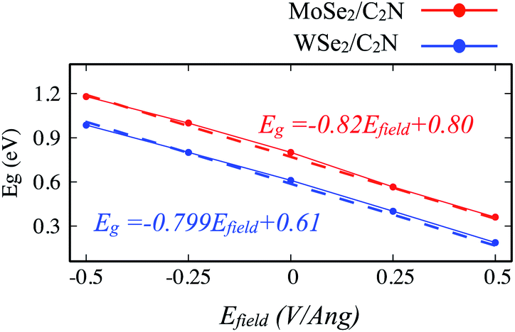 | ||
| Fig. 8 Variation of band gap values of heterostructure under applied vertical electrical field Efield. | ||
The positive direction of the electric field means that the applied field is pointing from MoSe2 (WSe2) layer towards C2N layer. At a positive electric field from 0.0 to 0.5 V Å−1, the band gap decreases from 0.8 eV (0.62 eV) to 0.53 eV (0.34 eV) for MoSe2/C2N (WSe2/C2N). While, at the negative electric field from −0.5 to 0.0 V Å−1, the band gap increases. This change in the band gap values is mainly due to the modification in the band alignment in presence of an electrical field, which implies a high sensitivity of the features of the heterostructure to an external electric field.
Indeed, it has been already proved from the previous theoretical calculations and experimental measurements that the external electric field can alter the band alignment of heterostructures.38,42 The variation in the band offsets at interface under an external electric field is shown in Fig. 9. When a positive electric field is applied, the VBM and CBM of MoSe2 (WSe2) layer trend to shift up with respect of the equilibrium fermi while the VBM and CBM of C2N layer shifts down (as shown in Fig. S4†), leading to an increase in VBO and CBO as demonstrated in Fig. 9. Similar trend is also observed at hetero-bilayers of TDMCs.43 In the case of a negative electrical field, the VBM (CBM) of MoS2 and C2N trend to shift toward each other leading to decreasing in VBO and CBO magnitude. More important, the type-II band alignment at C2N/MoSe2 and C2N/WSe2 heterostructures is also preserved upon applying a finite external electric field Efield range from −0.5 V Å−1 to 0.5 V Å−1.
 | ||
| Fig. 9 Variation in the ΔEc/ΔEv as a function of vertical electric field (Efield). | ||
4 Conclusion
In summary, I have studied the thermodynamic stability and electronic structures of C2N/MoSe2 and C2N/WSe2 heterostructures under the vertical strain and finite external electric field by using the DFT method. The interlayer distance and binding energy have demonstrated that the C2N monolayer holds with MoSe2 or WSe2 monolayer through the weak vdW interactions. This indicates that the formation of these heterostructures is exothermic. The band structures have shown that the heterostructures exhibit a narrower indirect band gap as compared to individual components, which boost the optical absorption over the visible and IR lights. The band alignment diagram has indicated the stabilization of a type-II band alignment configuration at heterostructures with large band offsets, implying a good performance of charge separation of photogenerated electron–hole pairs. The calculated Gibbs free energy of hydrogen adsorption have demonstrated a reduction in the overpotential, towards hydrogen evolution reaction, upon forming heterostructures, which is rationalized by charge transfer across interface. This indicates that the control of band offsets at interface can optimize the HER efficiency. The application of external perturbations includes the vertical strain and finite electrical field can modulate the band alignments. By applying a compressive strain, the band gap values have decreased and the band offsets have increased. Moreover, a similar trend has been observed upon applying a positive finite external electric field pointing from MoSe2 (WSe2) layer towards C2N layer. The magnitude of decrease/increase in the band gap energy/band offsets at MoSe2/C2N and WSe2/C2N heterostructures is bigger upon applying a finite electrical field than applying a vertical strain. The results have demonstrated that the type-II configuration at MoSe2/C2N and WSe2/C2N heterostructures is useful for photocatalytic water splitting towards hydrogen production. The applying either a vertical strain or a finite electrical field can bring an additional enhancement without switching the type-II band alignment configuration. The decrease in the band gap leads to a red shift in the absorption spectrum and allows to further harvest the IR and visible light as compared to individual components. The increase in the band offsets leads to strengthen the built-in electrical field across the interface; therefore, the separation of photo-generated electron–hole pairs would be more effective.Funding
This work was funded by EC through H2020-DT-NMBP-11-2020 project GA no. 953167 (OpenModel).Conflicts of interest
There are no conflicts to declare.Acknowledgements
I would like to acknowledge EC for funding through H2020-DT-NMBP-11-2020 project GA no. 953167 (OpenModel).The DFT calculations were supported by the Consortium des Equipements de Calcul Intensif (CECI), funded by the Fonds National de la Recherche Scientifique (F.R.S.-FNRS) under Grant 2.5020.11. I would like also to thank Prof. Jérôme Cornil (FNRS research director) and Dr Arrigo Calzolari (CNR Researcher) for their support.References
- J. Mahmood, F. Li, S.-M. Jung, M. S. Okyay, I. Ahmad, S.-J. Kim, N. Park, H. Y. Jeong and J.-B. Baek, An efficient and pH-universal ruthenium-based catalyst for the hydrogen evolution reaction, Nat. Nanotechnol., 2017, 12, 441–446, DOI:10.1038/nnano.2016.304.
- J. Mahmood, S.-M. Jung, S.-J. Kim, J. Park, J.-W. Yoo and J.-B. Baek, Cobalt Oxide Encapsulated in C2N-h 2D Network Polymer as a Catalyst for Hydrogen Evolution, Chem. Mater., 2015, 27, 4860–4864, DOI:10.1021/acs.chemmater.5b01734.
- J. Mahmood, E. K. Lee, M. Jung, D. Shin, I.-Y. Jeon, S.-M. Jung, H.-J. Choi, J.-M. Seo, S.-Y. Bae, S.-D. Sohn, N. Park, J. H. Oh, H.-J. Shin and J.-B. Baek, Nitrogenated holey two-dimensional structures, Nat. Commun., 2015, 6, 6486, DOI:10.1038/ncomms7486.
- H. Sahin, Structural and phononic characteristics of nitrogenated holey graphene, Phys. Rev. B: Condens. Matter Mater. Phys., 2015, 92, 085421, DOI:10.1103/PhysRevB.92.085421.
- M. R. Ashwin Kishore and P. Ravindran, Tailoring the Electronic Band Gap and Band Edge Positions in the C2N Monolayer by P and As Substitution for Photocatalytic Water Splitting, J. Phys. Chem. C, 2017, 121, 22216–22224, DOI:10.1021/acs.jpcc.7b07776.
- J. Li, A. Slassi, X. Han, D. Cornil, M. Ha-Thi, T. Pino, D. P. Debecker, C. Colbeau-Justin, J. Arbiol, J. Cornil and M. N. Ghazzal, Tuning the Electronic Bandgap of Graphdiyne by H-Substitution to Promote Interfacial Charge Carrier Separation for Enhanced Photocatalytic Hydrogen Production, Adv. Funct. Mater., 2021, 31, 2100994, DOI:10.1002/adfm.202100994.
- Z. Guan, C.-S. Lian, S. Hu, S. Ni, J. Li and W. Duan, Tunable Structural, Electronic, and Optical Properties of Layered Two-Dimensional C2N and MoS2 van der Waals Heterostructure as Photovoltaic Material, J. Phys. Chem. C, 2017, 121, 3654–3660, DOI:10.1021/acs.jpcc.6b12681.
- Z. Ma, S. Wang, C. Li and F. Wang, Strain engineering for C2N/Janus monochalcogenides van der Waals heterostructures: Potential applications for photocatalytic water splitting, Appl. Surf. Sci., 2021, 536, 147845, DOI:10.1016/j.apsusc.2020.147845.
- Y. Fan, S. Qi, W. Li and M. Zhao, Direct Z-scheme photocatalytic CO2 conversion to solar fuels in a two-dimensional C2N/aza-CMP heterostructure, Appl. Surf. Sci., 2021, 541, 148630, DOI:10.1016/j.apsusc.2020.148630.
- G. Wang, Z. Li, W. Wu, H. Guo, C. Chen, H. Yuan and S. A. Yang, A two-dimensional h-BN/C2N heterostructure as a promising metal-free photocatalyst for overall water-splitting, Phys. Chem. Chem. Phys., 2020, 22, 24446–24454, 10.1039/d0cp03925j.
- X. Luo, G. Wang, Y. Huang, B. Wang, H. Yuan and H. Chen, A two-dimensional layered CdS/C2N heterostructure for visible-light-driven photocatalysis, Phys. Chem. Chem. Phys., 2017, 19, 28216–28224, 10.1039/C7CP04108J.
- H. Wang, X. Li and J. Yang, The g-C3N4/C2N Nanocomposite: A g-C3N4-Based Water-Splitting Photocatalyst with Enhanced Energy Efficiency, ChemPhysChem, 2016, 17, 2100–2104, DOI:10.1002/cphc.201600209.
- R. Kumar, D. Das and A. K. Singh, C2N/WS2 van der Waals type-II heterostructure as a promising water splitting photocatalyst, J. Catal., 2018, 359, 143–150, DOI:10.1016/j.jcat.2018.01.005.
- A. Slassi, S. M. Gali, A. Pershin, A. Gali, J. Cornil and D. Beljonne, Interlayer Bonding in Two-Dimensional Materials: The Special Case of SnP3 and GeP3, J. Phys. Chem. Lett., 2020, 11, 4503–4510, DOI:10.1021/acs.jpclett.0c00780.
- A. El Haimeur, A. Slassi, A. Pershin, D. Cornil, M. Makha, E. Blanco, M. Dominguez and H. Bakkali, Reducing p-type Schottky contact barrier in metal/ZnO heterostructure through Ni-doping, Appl. Surf. Sci., 2021, 545, 149023, DOI:10.1016/j.apsusc.2021.149023.
- T. Su, Q. Shao, Z. Qin, Z. Guo and Z. Wu, Role of Interfaces in Two-Dimensional Photocatalyst for Water Splitting, ACS Catal., 2018, 8, 2253–2276, DOI:10.1021/acscatal.7b03437.
- D. S. Koda, F. Bechstedt, M. Marques and L. K. Teles, Tuning Electronic Properties and Band Alignments of Phosphorene Combined With MoSe2 and WSe2, J. Phys. Chem. C, 2017, 121, 3862–3869, DOI:10.1021/acs.jpcc.6b10976.
- Z. Zhang, Q. Qian, B. Li and K. J. Chen, Interface Engineering of Monolayer MoS2/GaN Hybrid Heterostructure: Modified Band Alignment for Photocatalytic Water Splitting Application by Nitridation Treatment, ACS Appl. Mater. Interfaces, 2018, 10, 17419–17426, DOI:10.1021/acsami.8b01286.
- G. Kresse and D. Joubert, From ultrasoft pseudopotentials to the projector augmented-wave method, Phys. Rev. B: Condens. Matter Mater. Phys., 1999, 59, 1758–1775, DOI:10.1103/PhysRevB.59.1758.
- G. Kresse and M. Marsman, VASP the GUIDE, 2012 Search PubMed.
- J. P. Perdew, K. Burke and M. Ernzerhof, Generalized Gradient Approximation Made Simple, Phys. Rev. Lett., 1996, 77, 3865–3868, DOI:10.1103/PhysRevLett.77.3865.
- S. Grimme, Semiempirical GGA-type density functional constructed with a long-range dispersion correction, J. Comput. Chem., 2006, 27, 1787–1799, DOI:10.1002/jcc.20495.
- M. Gajdoš, K. Hummer, G. Kresse, J. Furthmüller and F. Bechstedt, Linear optical properties in the projector-augmented wave methodology, Phys. Rev. B: Condens. Matter Mater. Phys., 2006, 73, 045112, DOI:10.1103/PhysRevB.73.045112.
- A. Calzolari, A. Catellani, M. Buongiorno Nardelli and M. Fornari, Hyperbolic Metamaterials with Extreme Mechanical Hardness, Adv. Opt. Mater., 2021, 9, 2001904, DOI:10.1002/adom.202001904.
- A. Slassi, N. Lakouari, Y. Ziat, Z. Zarhri, A. Fakhim Lamrani, E. K. Hlil and A. Benyoussef, Ab initio study on the electronic, optical and electrical properties of Ti-, Sn- and Zr-doped ZnO, Solid State Commun., 2015, 218, 45–48, DOI:10.1016/j.ssc.2015.06.010.
- M. Eaton, A. Catellani and A. Calzolari, VO2 as a natural optical metamaterial, Opt. Express, 2018, 26, 5342, DOI:10.1364/OE.26.005342.
- J. Sun, H. T. Wang, J. He and Y. Tian, Ab initio investigations of optical properties of the high-pressure phases of ZnO, Phys. Rev. B: Condens. Matter Mater. Phys., 2005, 71, 125132, DOI:10.1103/PhysRevB.71.125132.
- Y. Wang, A. Slassi, M.-A. Stoeckel, S. Bertolazzi, J. Cornil, D. Beljonne and P. Samorì, Doping of Monolayer Transition-Metal Dichalcogenides via Physisorption of Aromatic Solvent Molecules, J. Phys. Chem. Lett., 2019, 10, 540–547, DOI:10.1021/acs.jpclett.8b03697.
- Y. Zhao, S. M. Gali, C. Wang, A. Pershin, A. Slassi, D. Beljonne and P. Samorì, Molecular Functionalization of Chemically Active Defects in WSe2 for Enhanced Opto-Electronics, Adv. Funct. Mater., 2020, 30, 2005045, DOI:10.1002/adfm.202005045.
- A. Slassi, D. Cornil and J. Cornil, Theoretical characterization of the electronic properties of heterogeneous vertical stacks of 2D metal dichalcogenides containing one doped layer, Phys. Chem. Chem. Phys., 2020, 22, 14088–14098, 10.1039/D0CP01878C.
- A. Slassi and J. Cornil, Theoretical characterization of strain and interfacial electronic effects in donor-acceptor bilayers of 2D transition metal dichalcogenides, 2D Mater, 2018, 6, 015025, DOI:10.1088/2053-1583/aaf1d4.
- J. Shi, R. Tong, X. Zhou, Y. Gong, Z. Zhang, Q. Ji, Y. Zhang, Q. Fang, L. Gu, X. Wang, Z. Liu and Y. Zhang, Temperature-Mediated Selective Growth of MoS2/WS2 and WS2/MoS2 Vertical Stacks on Au Foils for Direct Photocatalytic Applications, Adv. Mater., 2016, 28, 10664–10672, DOI:10.1002/adma.201603174.
- Y. Wang, S. M. Gali, A. Slassi, D. Beljonne and P. Samorì, Collective Dipole-Dominated Doping of Monolayer MoS2: Orientation and Magnitude Control via the Supramolecular Approach, Adv. Funct. Mater., 2020, 30, 2002846, DOI:10.1002/adfm.202002846.
- J. He, K. Hummer and C. Franchini, Stacking effects on the electronic and optical properties of bilayer transition metal dichalcogenides MoS2, MoSe2, WS2 and WSe2, Phys. Rev. B: Condens. Matter Mater. Phys., 2014, 89, 075409, DOI:10.1103/PhysRevB.89.075409.
- Y. Liang, S. Huang, R. Soklaski and L. Yang, Quasiparticle band-edge energy and band offsets of monolayer of molybdenum and tungsten chalcogenides, Appl. Phys. Lett., 2013, 103, 042106, DOI:10.1063/1.4816517.
- E. Skúlason, V. Tripkovic, M. E. Björketun, S. Gudmundsdóttir, G. Karlberg, J. Rossmeisl, T. Bligaard, H. Jónsson and J. K. Nørskov, Modeling the Electrochemical Hydrogen Oxidation and Evolution Reactions on the Basis of Density Functional Theory Calculations, J. Phys. Chem. C, 2010, 114, 18182–18197, DOI:10.1021/jp1048887.
- D. Jiao, Y. Tian, H. Wang, Q. Cai and J. Zhao, Single transition metal atoms anchored on a C2N monolayer as efficient catalysts for hydrazine electrooxidation, Phys. Chem. Chem. Phys., 2020, 22, 16691–16700, 10.1039/D0CP02930K.
- A. Slassi, P. B. Sorokin and A. Pershin, Ohmic/Schottky barrier engineering in metal/SnP3 heterostructures, J. Alloys Compd., 2020, 831, 154800, DOI:10.1016/j.jallcom.2020.154800.
- S. Deng, L. Li and P. Rees, Graphene/MoXY Heterostructures Adjusted by Interlayer Distance, External Electric Field, and Strain for Tunable Devices, ACS Appl. Nano Mater., 2019, 2, 3977–3988, DOI:10.1021/acsanm.9b00871.
- J. Yu, M. Zhou, M. Yang, Q. Yang, Z. Zhang and Y. Zhang, High-Performance Borophene/Graphene Heterostructure Anode of Lithium-Ion Batteries Achieved via Controlled Interlayer Spacing, ACS Appl. Energy Mater., 2020, 3, 11699–11705, DOI:10.1021/acsaem.0c01808.
- L. Zhang, Y. Tang, A. R. Khan, M. M. Hasan, P. Wang, H. Yan, T. Yildirim, J. F. Torres, G. P. Neupane, Y. Zhang, Q. Li and Y. Lu, 2D Materials and Heterostructures at Extreme Pressure, Adv. Sci., 2020, 7, 2002697, DOI:10.1002/advs.202002697.
- Z. Chen, X. Ma, J. Hu, F. Wan, P. Xu, G. Wang, M. Wang, S. Deng and C. Huang, Band alignment of Zr2CO2/MoS2 heterostructures under an electric field, New J. Chem., 2021, 45, 16520–16528, 10.1039/D1NJ02440J.
- W. Li, T. Wang, X. Dai, X. Wang, C. Zhai, Y. Ma, S. Chang and Y. Tang, Electric field modulation of the band structure in MoS2/WS2 van der waals heterostructure, Solid State Commun., 2017, 250, 9–13, DOI:10.1016/j.ssc.2016.11.006.
Footnote |
| † Electronic supplementary information (ESI) available. See https://doi.org/10.1039/d2ra00847e |
| This journal is © The Royal Society of Chemistry 2022 |