DOI:
10.1039/D2RA00611A
(Paper)
RSC Adv., 2022,
12, 7821-7829
Multi-mode surface plasmon resonance absorber based on dart-type single-layer graphene
Received
29th January 2022
, Accepted 3rd March 2022
First published on 9th March 2022
Abstract
In this paper, a multi-mode surface plasmon resonance absorber based on dart-type single-layer graphene is proposed, which has the advantages of polarization independence, tunability, high sensitivity, high figure of merit, etc. The device consists of a top layer dart-like patterned single-layer graphene array, a thicker silicon dioxide spacer layer and a metal reflector layer, and has simple structural characteristics. The numerical results show that the device achieves the perfect polarization-independent absorption at the resonance wavelengths of λI = 3369.55 nm, λII = 3508.35 nm, λIII = 3689.09 nm and λIV = 4257.72 nm, with the absorption efficiencies of 99.78%, 99.40%, 99.04% and 99.91%, respectively. The absorption effect of the absorber can be effectively regulated and controlled by adjusting the numerical values such as the geometric parameters and the structural period p of the single-layer graphene array. In addition, by controlling the chemical potential and the relaxation time of the graphene layer, the resonant wavelength and the absorption efficiency of the mode can be dynamically tuned. And can keep high absorption in a wide incident angle range of 0° to 50°. At last, we exposed the structure to different environmental refractive indices, and obtained the corresponding maximum sensitivities in four resonance modes, which are SI = 635.75 nm RIU−1, SII = 695.13 nm RIU−1, SIII = 775.38 nm RIU−1 and SIV = 839.39 nm RIU−1. Maximum figure of merit are 54.03 RIU−1, 51.49 RIU−1, 43.56 RIU−1, and 52.14 RIU−1, respectively. Therefore, this study has provided a new inspiration for the design of the graphene-based tunable multi-band perfect metamaterial absorber, which can be applied to the fields such as photodetectors and chemical sensors.
1. Introduction
The perfect metamaterial absorber (PMA) is a new type of artificial absorber developed in recent years, which can achieve good impedance matching with free space to reduce the reflection of incident electromagnetic waves.1–3 Therefore, it can generate strong coupling with the electromagnetic component of the incident electromagnetic wave, perfectly absorb the electromagnetic wave incident on the specific wave band of PMA, and is widely used in optical sensing, optical stealth, photodetector, photothermal conversion, catalysis and so on.4–7
Graphene, as a new type of two-dimensional material, has great research value in optical and electrical properties.8–12 Graphene has extremely high carrier mobility,13,14 full-spectrum response to light in the ultraviolet to terahertz band, and ultra-fast response to light, so it is one of the most promising materials for designing wave absorbing devices. However, the absorption performance of single-layer graphene in visible light and near-infrared bands is poor, only 2.3%,15–17 which limits quantum efficiency and its application in optoelectronic devices. Through, graphene has a strong surface plasmon resonance, and the technology based on surface plasmon resonance can make it have the ability to break through the traditional optical diffraction limit, and has the characteristic of local enhancement of electromagnetic field, thus achieving perfect absorption. Among the numerous applications of surface plasmon polaritons, the research of surface plasmon wave absorber and its refractive index sensing characteristics has been attracting people's attention. For example, in 2017 Zare et al.18 A graphene-based absorbent with two absorption peaks in the near infrared band is proposed. The results show that when only one layer of graphene is used, the surface plasmon resonance (SPR) in the groove amplifies the interaction between light and graphene, and the absorption of the structure increases to more than 0.9. In 2019, Luo et al. A mid-infrared tunable dual-frequency polarization insensitive coherent perfect wave absorber is proposed. Through the design of double-layer graphene waveguide, polarization insensitive dual-frequency ideal absorption peaks were obtained at 9611 nm and 9924 nm.19 In 2020, Wu proposed and studied a dual-band polarization insensitive tunable graphene absorber consisting of a square graphene ring.20 Two absorption peaks of 99.87% and 97.82% were observed at 3.92 THz and 6.96 THz respectively. However, most of the research focuses on single-band and dual-band narrow-band perfect absorbers, while the research on multi-band ideal narrow-band perfect absorbers is relatively less.21–24 This is because of the strict limitation, which makes it difficult to realize the narrow band perfect absorber of multi-band with simple absorber structure.
In this paper, a four-mode surface plasmon resonance absorber based on dart-like single-layer graphene is designed and studied. The absorber consists of dart-like patterned single-layer graphene array at the top, thick SiO2 spacer layer and metal mirror layer. Perfect polarization-independent absorption was achieved at λI = 3369.55 nm, λII = 3508.35 nm, λIII = 3689.09 nm and λIV = 4257.72 nm, and the absorption efficiency reached 99.78%, 99.40%, 99.04% and 99.91% respectively. In addition, impedance matching diagram and electric field intensity distribution diagram were drawn, and the mechanism of perfect absorption was studied. Then, the effects of geometric parameters and structural period on four-band absorption performance are studied. Moreover, the tunable characteristics of the absorber are proved by changing Fermi level and relaxation time. Finally, the sensing performance of the device is studied by changing the ambient refractive index, and the highest figure of merit and sensitivity of the absorber are 54.03 RIU−1 and 839.39 nm RIU−1, respectively. It is worth mentioning that compared with other graphene structures, our proposed structure has the advantages of more flexible and variable geometric parameters and more sensitive sensing performance, which greatly promotes the diversity of graphene-based metamaterial resonant absorber design. Therefore, we believe that this kind of absorbing material has potential applications prospects in the fields of sensors, modulators and detectors.
2. Structure design and numerical model
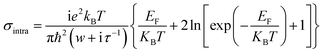
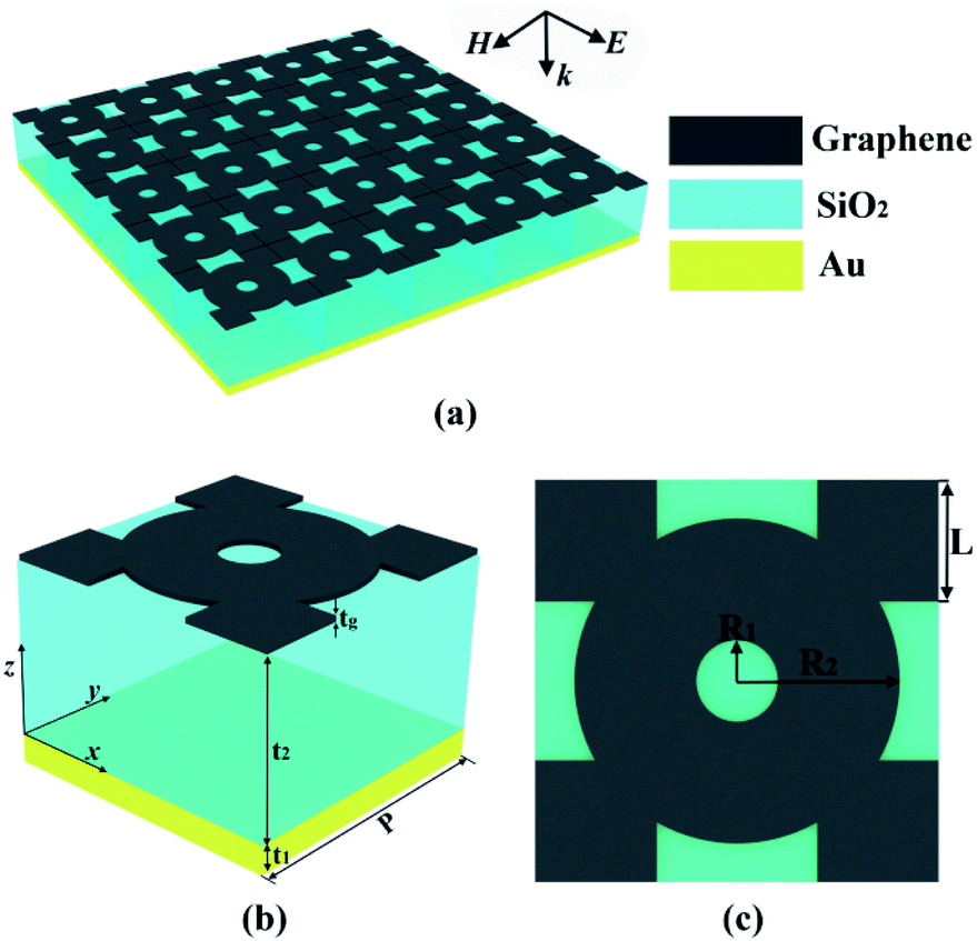
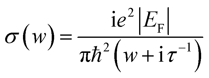
As shown in Fig. 1(a), the whole structure of a perfect absorber with high sensitivity and multi-band dart-shaped monolayer graphene array with specific parameters is shown. The incident wave hits the surface of the absorber structure in the vertical downward propagation direction, forming multi-mode SPR. Graphene layer is located on top of the dielectric silicon dioxide (SiO2) layer and the metal mirror (Au) layer, forming a sandwich stacked structure. In the simulation, the refractive index of the SiO2 dielectric layer is 1.97. The material parameters of Au layer are selected according to Drude conductivity model, with dielectric constant ε∞ = 1.0, working frequency ωp = 1.37 × 10¹⁶ s−1 and collision frequency γ = 4.32 × 10¹⁴ s−1.25,26 Multi-mode SPR is realized by changing different structure and material parameters. As shown in Fig. 1(b), it is a three-dimensional diagram of the unit structure of the wave absorber, showing the frame structure of the wave absorber. Thickness of Au layer t1 = 200 nm, thickness of SiO2 layer t2 = 1200 nm and structure period Px = Py = 1250 nm. Based on this, the finite difference time domain (FDTD) method is used to simulate and analyze the model structure.27–29 In the process, periodic boundary conditions are selected in the X and Y directions, and 24 layers of perfect matching layer (PML) are added in the Z axis direction, and the wavelength of the incident light is set in the mid-infrared band of 3000 nm to 5000 nm. Fig. 1(c) is a top view of periodic monolayer graphene array deposited on SiO2/Au substrate, showing the details of dart graphene parameters. The inner radius R1 = 30 nm, the outer radius R2 = 180 nm, and the square squares L = 200 nm. The graphene SPR mechanism is used to realize multi-mode perfect absorption.30–32 In addition, the expression of dielectric constant of dart-type single-layer graphene is:33,34| |
 | (1) |
| |
 | (2) |
where: e = 1.6 × 10⁻¹⁹ C is the charge of the electron, KB = 1.381 × 10⁻²³ J K−1 is the boltzmann constant, T = 300 K is the ambient room temperature, ħ = h/2π = 1.05 × 10⁻³⁴ J s is the reduced Planck constant, w represents the angular frequency of the incident wave, EF and τ represent the Fermi level and the relaxation time of the graphene layer.
 |
| | Fig. 1 (a) A 3D schematic diagram of the whole structure of a perfect wave absorber with a periodic monolayer graphene array; (b) three-dimensional structure diagram of dart type single-layer graphene array wave absorber unit structure; (c) top plan view of dart graphene deposited on SiO2/Au substrate. The geometric parameters of the structure are t1 = 200 nm, t2 = 1200 nm, Px = Py = 1250 nm, R1 = 30 nm, R2 = 180 nm, L = 200 nm and tg = 1.0 nm. | |
In the infrared band, according to Pauli incompatibility principle EF ≫ ħw, the inter-band contribution of graphene conductivity can be neglected, and the surface conductivity of graphene mainly depends on the in-band contribution. Therefore, at room temperature, the σintra is mathematically solved and transformed into Drude conductivity form, and the total conductivity of graphene can be written as:35,36
| |
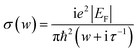 | (3) |
The wave vector of graphene surface plasma depends on the total conductivity. According to eqn (3), the conductivity of graphene depends on Fermi level, so the plasma absorber based on graphene can be dynamically adjusted by changing Fermi level and relaxation time without changing its geometric structure.37,38 According to the material parameters of the modulated graphene layer, it is found that when EF = 0.6 eV and τ = 0.6 Ps, the best multimode surface plasmon resonance is achieved. The absorption efficiency is defined as A = 1 − R − T where R and T are the reflection efficiency and the transmission efficiency, respectively.39,40 Obviously, when the reflection efficiency and transmission efficiency are small enough, the absorption efficiency is the largest. In this paper, the thickness (200 nm) of the metal reflective layer is much greater than its skin depth, which is enough to suppress the transmission of all waves, so the transmission efficiency (T) is almost zero,41,42 and the absorption efficiency can be defined as A = 1 − R. When the graphene surface plasmon resonance occurs, the reflection efficiency R = 0, which means that the total incident light power is absorbed. Therefore, A = 1, which theoretically realizes the perfect absorption of the wave absorber. In actual experiments, gold film and silicon dioxide isolation layer can be deposited on silicon substrate by electron beam evaporation, and then graphene layer can be grown on copper catalyst by chemical vapor deposition. Through electron beam lithography and oxygen plasma etching,43 the dart type single-layer graphene wave absorber was prepared.
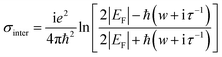
Fig. 2(a) shows the absorption spectrum of graphene absorber with dart structure formed by ring, column and ring + column. Fig. 2(b) and (c) show the top view of the single-structure graphene absorber with rings and columns. Undoubtedly, by combining the ring and the cylinder, the absorption of graphene in the mid-infrared band is significantly improved, and at the same time, the absorption band is increased, thus improving the absorption efficiency. Based on this dart-type structure, the graphene absorber achieves the perfect polarization-independent absorption at λI = 3369.55 nm, λII = 3508.35 nm, λIII = 3689.09 nm and λIV = 4257.72 nm, respectively. With the absorption efficiencies of 99.78%, 99.40%, 99.04% and 99.91%, respectively, corresponding to Mode I, Mode II, Mode III and Mode IV. When the infrared light is incident vertically into the structure, the dart graphene is excited to generate surface plasmon, and the incident light at four modes wavelengths is strongly limited by graphene. At this time, the incident light wave is consistent with the free electron frequency on the surface of graphene, which causes the phenomenon of SPR. The light wave consumes energy to excite the plasma oscillation, and the energy of the incident wave is strongly absorbed, thus achieving perfect absorption.6,37
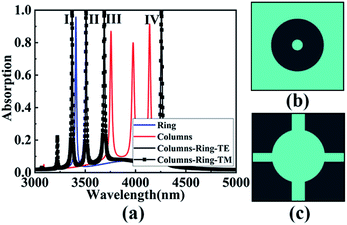 |
| | Fig. 2 (a) Absorption spectra of circular rings, cylinders and graphene absorbers with dart-type structures; (b) a top view of a graphene absorber with a circular ring structure, wherein the inner radius is R1, and the outer radius is R2; (c) top view of a graphene absorber with a cylindrical structure and a width of L. The structure periods are all P. | |
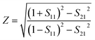
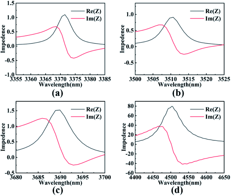
Impedance matching principle is an important theoretical factor to ensure the perfect absorption of wave absorber. Fig. 3(a)–(d) show the functional relationship between the effective impedance of the absorber and the incident wavelengths of different modes I–IV. According to the effective impedance theory of ideal wave absorber:44,45
| |
 | (4) |
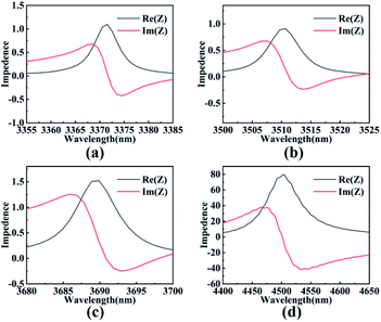 |
| | Fig. 3 Effective impedance matching diagram amplification of the resonance modes I (a), II (b), III (c) and IV (d) of the dart-type single-layer graphene perfect absorber. The black line represents the real part and the red line represents the imaginary part. | |
In the equation, S11 and S21 are related to the reflection coefficient and transmission coefficient, respectively. From the point of view of impedance matching, when the effective impedance of the absorber is matched with the impedance of the free space, the reflection of the structure can be significantly reduced (S11 = 0) and perfect absorption can be achieved. According to the impedance matching relationship shown in Fig. 3 and the absorption spectrum, it can be seen that due to the surface plasmon resonance of graphene layer, the wave absorber can achieve perfect absorption of 99.78%, 99.40%, 99.04% and 99.91% in four wave bands.
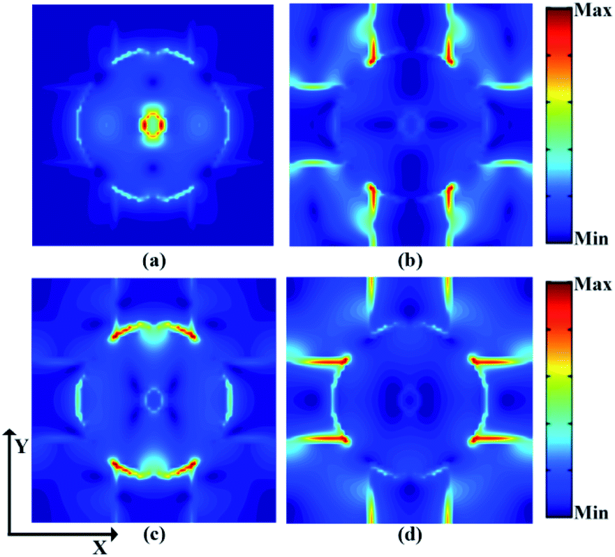
In order to further understand the principle of multi-mode perfect absorption, we placed the electric field monitor at the four resonance wavelengths λI = 3369.55 nm, λII = 3508.35 nm, λIII = 3689.09 nm and λIV = 4257.72 nm, and obtained the X–Y cross-sectional electric field distribution as shown in Fig. 4. Obviously, for the resonance modes I and III, the electric field in the X–Y direction is mainly confined to the center of the ring, which can consume the incident light energy more effectively to maintain the local electromagnetic field, and then generate the resonance absorption effect. For resonance modes II and IV, the electric field in the X–Y direction is mainly distributed at the inner edge of the fourth ring pillar, which is mainly due to the coupling between the vibration frequency of the dart graphene layer and the wavelength of the incident light. And provides electric dipole resonance, which consumes the energy of the incident light, thus achieving perfect absorption. This is consistent with the absorption effect of the ring and the ring column in Fig. 2. At the same time, the edges of the ring and the ring column also have the characteristics of local electromagnetic field, and the local absorption of the combined darts graphene can lead to stronger light absorption.
 |
| | Fig. 4 (a)–(d) Show the cross-sectional electric field distribution in the X–Y direction of the wave absorber surface when the incident light wavelengths are λI = 3369.55 nm, λII = 3508.35 nm, λIII = 3689.09 nm and λIV = 4257.72 nm, respectively. | |
3. Results and discussions
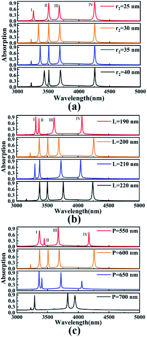
We studied the effects of the geometric parameters (the inner diameter R1 of the ring, the edge length L) and the structural period P of the dart-shaped graphene array on the absorption spectrum of the absorber by using the method of controlling variables. The corresponding absorption spectra are shown in Fig. 5. Obviously, when the inner diameter R1 of the ring increases from 25 nm to 40 nm (as shown in Fig. 5(a)), the absorption efficiency of the resonant mode I of the absorber increases first and then decreases, and the absorption of other resonant modes hardly changes. This is because the change in the inner diameter R1 of the ring affects only the SPR in the resonance mode I. When R1 = 30 nm, the absorption of resonance mode I reaches the maximum of 99.78%, and then the local electromagnetic field on the graphene surface has the strongest ability, reaching the critical saturation.46 At the same time, the absorption peak in resonance mode I undergoes a significant red shift, which is due to the change of the position of the circular hole in the graphene structure. Thus, in practical application, more benefits can be provided by varying the inner diameter parameter R1. Next, Fig. 5(b) shows the effect of the edge length l on the performance of the absorber as the edge length l increases from 190 nm to 220 nm. For resonance modes I, II and IV, the change trends of the absorption wavelengths of the light is the same, which is a quasi-sinusoidal changes with first red shift and then blue shift. For the resonant mode III, the resonant wavelength shows a slight red shift with the increase of L. This is due to the change of the edge length L, which changes the distribution position of the plasma on the surface of the dart-type graphene. At the same time, when L = 200 nm, the four resonance modes reach the critical saturation, and the absorption efficiency reaches the perfect absorption, which is 99.78%, 99.40%, 99.04% and 99.91%, respectively. This means that the edge length L has multiple selectivities, and the specified spectral response can be obtained through appropriate selection under the condition of uniform and efficient absorption. Therefore, it provides a more flexible choice for shock absorbers in practical applications.
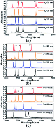 |
| | Fig. 5 When other parameters remain unchanged. (a) When the inner diameter R1 of the ring increases from 25 nm to 40 nm, the corresponding absorption spectrum is obtained; (b) When the edge length L of the ring column increases from 190 nm to 220 nm, the corresponding absorption spectrum is obtained; (c) When the structure period P increases from 550 nm to 700 nm, the corresponding absorption spectrum is obtained. | |
Fig. 5(c) shows the change of the absorption spectrum when the structure period P is increased from 550 nm to 700 nm. Since the absorption of single-layer graphene depends to a large extent on its natural frequency, we can then control the period of the structure to obtain the perfect absorption of graphene. It can be seen that when the period P of the dart-type graphene absorber is changed, the resonance absorption is changed significantly. For the resonance mode I, the blue shift occurs when the P is greater than 650 nm, and the absorption efficiency is significantly reduced. The changes of the absorption spectra in resonance modes II and IV are consistent with the first red shift and then blue shift, and the absorption efficiency increases first and then decreases. For the absorption wavelength in resonance mode III, when the structure period P is greater than 650 nm, a red shift occurs, and the absorption efficiency increases first and then decreases. This is because the absorption of the incident light field by the plasma resonance mode on the surface of the dart-type graphene absorber array undergoes unsaturated, critical saturated and supersaturated states. Obviously, when the structure period P = 600 nm, the critical coupling state is reached, and the maximum incident light absorption of dart-type graphene is enhanced, achieving the perfect absorption in the four bands. However, when it increases gradually, the surface plasmon resonance of the structure reaches supersaturation, and most of the incident light field is not localized and absorbed by the resonant mode in the center of the resonant cavity.47
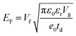
For the absorber with fixed structure parameters, dynamic tunability has more important application value. As shown in Fig. 6, when the structure of the absorber is fixed, we studied the changes of the absorption spectrum of the absorber by respectively changing the Fermi level and the relaxation time of the graphene layer. The EF formula of the Fermi energy level of graphene is as follows:25,48–50
| |
 | (5) |
where
Vg is the applied voltage (which can be controlled by changing the gate voltage or chemical doping),
e0 is the amount of electron charge,
Vf is the Fermi speed (
Vf=
c/300,
c is the speed of light in vacuum),
td is the thickness of the dielectric layer, and
ε0 and
εr respectively represent the vacuum dielectric constant and relative dielectric constant.
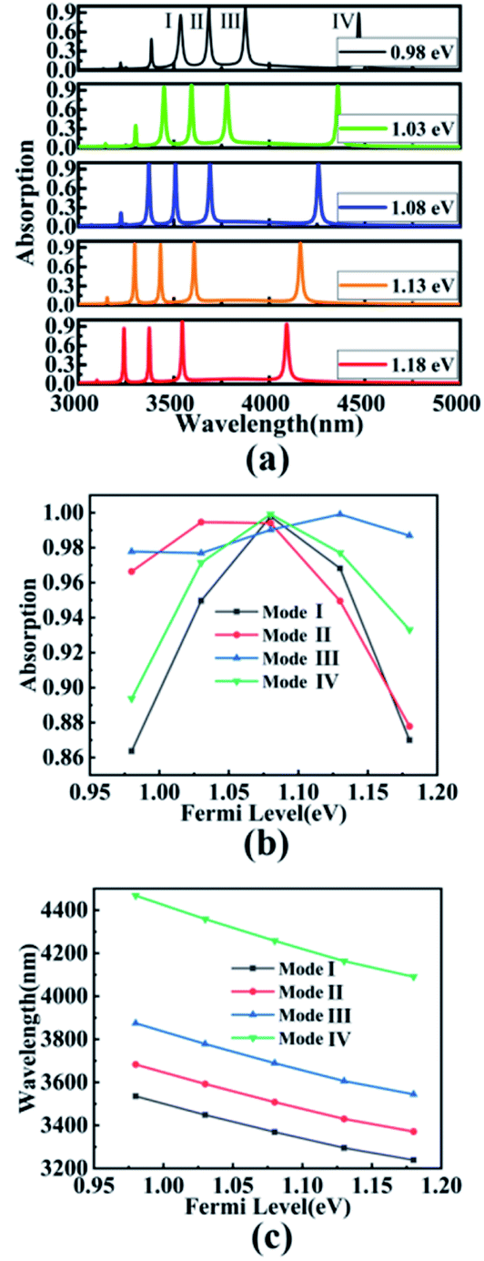
Fig. 6(a) shows that with the Fermi level increasing from 0.98 eV to 1.18 eV, the wavelengths of the four resonant modes of the absorber are blue shifted. It can be seen that the blue shift is more obvious for the long-wave resonance mode. This is because the resonant wavelength of the wave absorber can be expressed as:

. In which
L and
C respectively represent the inductance and capacitance in the wave absorber. With the increase of
EF,
L will decrease, resulting in blue shift of resonance wavelength. At the same time, the resonant wavelength can also be expressed as:
λres =
α +
β ×
nsp. Where
α and
β are coefficients closely related to the geometric shape of the model and the surrounding dielectric properties,
51,52 and
nsp represents the effective refractive index of graphene. Therefore, with the increase of Fermi level, the effective refractive index
nsp of graphene SPR decreases, and the resonant wavelength
λres decreases, resulting in blue shift.
Fig. 6(b) and (c) show the intensity spectra and wavelength shifts of the absorption peaks in the four resonance modes, respectively, during the change of Fermi level. It can be clearly seen that with the increase of the Fermi level, for Mode I, the absorption peak increases first and then decreases. The resonance wavelength shifts from 3239.45 nm blue to 3535.93 nm, with a maximum absorption efficiency of 99.78% at
EF = 1.08 eV. The resonance wavelength can be approximately expressed as
λI = (−1493.28
EF + 4990.65) nm. For mode II, the resonance wavelength shifts from 3371.57 nm blue to 3683.05 nm, and the absorption efficiency is 99.46% at
EF = 1.03 eV. The resonance wavelength can be approximately expressed as
λII = (−1570.36
EF + 5213.11) nm. For mode III, the resonance wavelength shifts from 3544.85 nm blue to 3874.72 nm, with a maximum absorption efficiency of 99.92% at
EF = 1.13 eV. The resonance wavelength can be approximately expressed as
λIII = (−1663.68
EF + 5495.43) nm. For mode IV, the resonance wavelength shifts from 4090.41 nm blue to 4467.51 nm, and the absorption efficiency is 99.91% at
EF = 1.13 eV. The resonance wavelength can be approximately expressed as
λIV = (−1898.96
EF + 6318.31) nm. To sum up, for the four resonance modes, when
EF reaches 1.13 eV, the average efficiency of the four absorption peaks is the highest, all of which achieve perfect absorption. Moreover, with the increase of Fermi level, the resonance of SPR will reach the maximum. However, with the continuous increase of
EF, the SPR region has reached supersaturation, resulting in a decrease of absorption.
53 Therefore, compared with the noble metal absorber, the device can adjust the absorption spectrum by adjusting the Fermi level of the graphene layer, without changing the geometric shape of the absorber, which is more valuable in practical application.
 |
| | Fig. 6 The geometry structure of the fixed wave absorber. (a) Only increases the Fermi level of graphene from 0.98 eV to 1.18 eV to obtain the absorption spectrum; (b) and (c), the absorption peak intensity spectra and wavelength offsets of the four resonant modes are calculated, respectively. | |
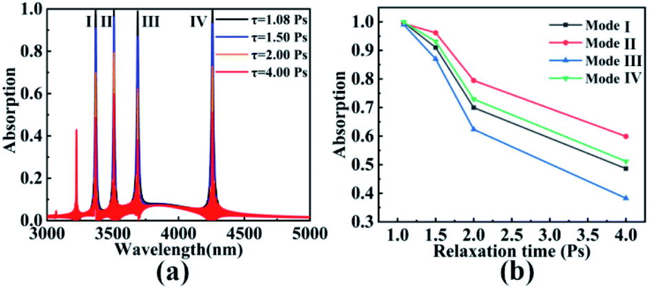
The electronic relaxation time τ of the dart-type graphene layer can be expressed as:54,55
In the equation, EF and v represent the Fermi level and carrier mobility of graphene, respectively; e represents the electronic charge; vF = 106 m s−1 is the Fermi velocity. Fig. 7(a) shows the absorption spectrum of the absorber when the relaxation time τ increases from 1.08 Ps to 4.00 Ps. It can be clearly seen that the wavelength of the resonance mode does not change with the increase of the relaxation time. While the absorption efficiency of the four resonance modes continuously decreases. This is because at τ = 1.08 Ps, plasmon resonance has reached critical saturation, and with the increase of relaxation time, most of the incident light wave is reflected back, and the electromagnetic wave energy absorbed by resonance continuously decreases. Fig. 7(b) calculates the change of absorption intensity of four modes with the increase of relaxation time from 1.08 Ps to 4.00 Ps. Among them, the absorption modulation ranges of the four resonance modes are 48.64–99.78% (Mode I), 59.90–99.40% (Mode II), 38.26–99.04% (Mode III) and 51.19–99.91% (Mode IV), respectively. Furthermore, the modulation depths of absorption efficiency corresponding to the four modes are 51.14%, 39.50%, 60.78% and 48.72%, respectively. Therefore, the dart-type single-layer graphene absorber we proposed is very sensitive to the change of electron relaxation time. In practical application, we can place organic molecules on the surface of graphene layer, which can significantly improve the carrier mobility v, thus affecting the change of relaxation time.52
 |
| | Fig. 7 The absorption spectrum of the absorber when the geometry structure of the absorber. (a) Only increases the relaxation time τ from 1.08 Ps to 4.00 Ps. (b) The changes of absorption intensity of the four modes in the process of relaxation time are calculated. | |
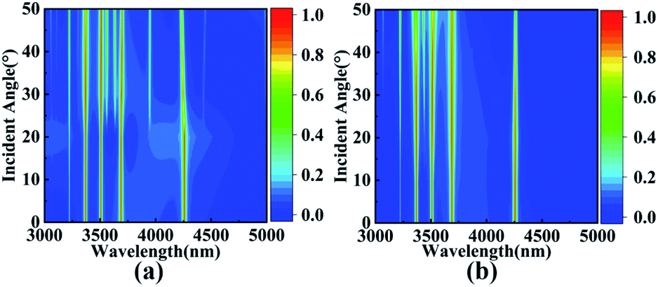
In practical application, it is often not only a single vertical incident plane wave. Therefore, it is extremely important that the absorber exhibit insensitivity to oblique incidence. On this basis, as shown in Fig. 8, under the TE polarization and TM polarization, the spectral changes of multi-mode absorption of the dart-type graphene absorber were investigated by changing the angle of incidence of the light source from 0° to 50°. Obviously, as shown in Fig. 8(a), for Modes I, II and III under TE polarization, the resonance wavelength hardly changes as the incident angle increases to 50°. And maintains a perfect absorption of more than 95%. For the resonance mode IV, the resonance wavelength undergoes a slight blue shift, because in this mode, the dielectric constant of the waveguide layer decreases with the increasing angle of incidence. Furthermore, the effective refractive index of the dart-type graphene surface plasma is reduced, resulting in the blue shift of the resonance wavelength.47 Meanwhile, as shown in Fig. 8(b), under the TM polarization, the resonant wavelengths of the four modes of the absorber almost do not change with the increasing incidence angle. Perfect absorption remained above 95% for Modes I, II, and III. For mode IV, a significant reduction in absorption intensity occurred at 40°. This is because in this mode, the absorber absorption becomes more incident angle and polarization dependent for larger incident angles, but the resonant wavelength remains almost constant. The contact area between the incident light wave and the dart-type graphene layer decreases with the increase of the incident angle, and the intensity of plasma resonance is weakened, resulting in the reduction of absorption efficiency. However, at the angle of incidence of 50°, the absorption efficiency of the resonant mode IV is still greater than 90%. For different polarization, the changes of the four absorption peaks are not significant with the increase of the incident angle of the light source, which proves that the designed dart-type graphene absorber is insensitive to the angle. In practice, we can manually design the concave structure, attach the wave absorber to its surface, and realize the wave absorption of incident light at a certain angle through the concave structure, which provides more possibilities for the practical application of the device. It is worth mentioning that the absorber studied has the obvious advantages of simple structure and high stability, which indicates that the absorber has extremely important value in the practical application of integrated optoelectronic devices.
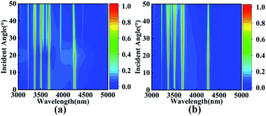 |
| | Fig. 8 Absorption spectrogram of light source incident angle increased from 0° to 50° under TE polarization (a) and TM polarization (b). | |
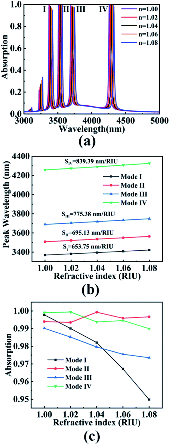
It can be found that the resonant absorption peak of the absorber studied in this paper has the characteristics of narrow bandwidth and multi-bands. As shown in Fig. 9, the sensing performance of the absorber was studied. The plasma generated on the surface of the dart-type graphene absorber structure is sensitive to the change of the external refractive index, and the resonant mode wavelength of the absorber changes along with the change of the refractive index. Based on this, in the actual application process, the absorber proposed in this paper can be used in the range of refractive index sensor. Fig. 9(a) is a graph showing changes in the absorption spectrum of the absorber as the ambient refractive index n increases from 1.00 to 1.08 (interval 0.02). It can be seen that with the increase of n, the wavelengths of the four resonance modes will undergo red shift, and the variation amplitude of the absorption efficiency is very small. As shown in Fig. 9(b) and (c), the wavelength shift and the absorption peak intensity change spectra of the four resonance modes during the change of the environmental refractive index n are calculated. Four modes of wavelength red shift can be observed, which are 3369.55–3421.85 nm (Mode I), 3508. 35–3563. 96 nm (Mode II), 3689.09–3748.12 nm (Mode III) and 4257.72–4326.87 nm (Mode IV), respectively. In addition, the absorption efficiency of the four resonance modes of the absorber is still above 95% in the process of the change of environmental refractive index. Due to the plasma generated on the surface of the graphene absorber structure, when the frequency of the free electrons and the photon is the same, an plasmon resonance phenomenon will be generated, resulting in the enhancement of the local electric field. At this time, the reflectivity of the incident light decreases until it approaches 0, and the incident light is absorbed by the structure.
 |
| | Fig. 9 (a) Absorption spectra of mode I, mode II, mode III and mode IV with different refractive indices; (b) linear relationship between resonant wavelength and refractive index; (c) linear relationship between absorption peak and refractive index. | |
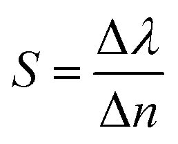
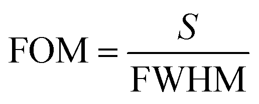
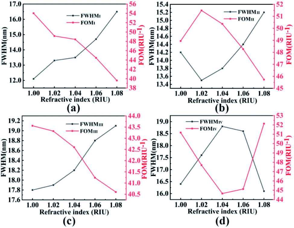
Next, as shown in Fig. 10(a)–(d), the full width at half maximum (FWHM) of the absorption peaks in the four resonance modes are calculated to be 12.1 nm (Mode I), 13.5 nm (Mode II), 17.8 nm (Mode III) and 16.1 nm (Mode IV), respectively. In order to further study the sensing performance of the absorber, the sensitivity (S) and figure of merit (FOM) are defined as follows:48,56
| |
 | (7) |
| |
 | (8) |
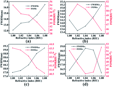 |
| | Fig. 10 Shows FWHM and FOM of resonance mode I (a), resonance mode II (b), resonance mode III (c) and resonance mode IV (d) when the ambient refractive index n increases from 1.00 to 1.08. | |
In the equation, Δλ refers to the change in resonance wavelength, Δn representing the change in ambient refractive index. According to eqn (7), the slope of the straight line in Fig. 9(b) can be obtained as the sensitivity of this wave absorber. The calculated sensitivities for the four modes are 653.75 nm RIU−1, 695.13 nm RIU−1, 775.38 nm RIU−1, and 839.39 nm RIU−1. FOM can quantify the sensitivity of the sensor. Based on this, according to formula (8), FOM of four resonance modes is obtained as shown in Fig. 10. The maximum FOM for the four resonance modes were 54.03 RIU−1, 51.49 RIU−1, 43.56 RIU−1, and 52.14 RIU−1, respectively. Through comparison, our wave absorber has better sensitivity and FOM, and has the characteristics of dynamic adjustment, polarization independence and angle insensitivity, as shown in Table 1.57–61 The results show that the sensitivity sensor designed by us has better sensing performance and wider application prospect.
Table 1 Comparison of this absorber with other similar single-layer graphene absorbers
| References |
57 |
58 |
59 |
60 |
61 |
Proposed |
| FOM/RIU−1 |
4.68 |
25 |
68.57 |
34.3 |
9.9 |
54.03 |
| S nm−1 RIU−1 |
600 |
190 |
596 |
282 |
587.8 |
839.39 |
4. Conclusion
In summary, a multi-mode surface plasmon resonance absorber based on dart-type single-layer graphene was studied in this paper. Which consists of a top layer dart-like patterned single-layer graphene array, a thicker PMMA spacer layer and a metal reflector layer and has simple structural characteristics. The perfect polarization-independent absorption at the wavelengths of λI = 3369.55 nm, λII = 3508.35 nm, λIII = 3689.09 nm and λIV = 4257.72 nm is studied by the FDTD simulation software. At the same time, the reason why the device realizes perfect multi-band absorption in mid-infrared is demonstrated from the impedance matching principle and internal electric field analysis. Moreover, by controlling the geometric and intrinsic parameters of the graphene layer, the resonant wavelengths and absorption efficiencies of the four modes can be dynamically tuned. At the same time, the sensing performance of the device was studied by changing the environmental refractive index, and the highest FOM and S of the absorber were 54.03 RIU−1 and 839.39 nm RIU−1, respectively. Therefore, the device has important application potential and application value in the aspects of photoelectric detection, chemical sensing and the like.
Conflicts of interest
There are no conflicts to declare.
Acknowledgements
The authors are grateful to the support by the National Natural Science Foundation of China (Grant No. 11604311, 61705204, 21506257, 12074151, 11875228, 61975171), the Funded by the Scientific Research Fund of Sichuan Provincial Science and Technology Department (Grant No. 2020YJ0137 and 2020YFG0467), the Funded by Southwest University of Science and Technology Undergraduate Innovation and Entrepreneurship Training Program Project (No. S202110619065, S202010619020, S202110619007), the Funded by the Undergraduate Innovation Fund Project Funding by Southwest University of Science and Technology (No. CX 21-008), the Funded by Talent Training and Laboratory Open Innovation Project of SWUST Institute of Science (No. LX20210001), the Funded by Major Special Projects of Science and Technology in Fujian Province (2021HZ021027), the Funded by teaching reform project of College Physics Teaching Committee of the Ministry of Education (DJZW202034XN).
References
- Y. P. Qi, C. Q. Liu, B. B. Hu, X. Y. Deng and X. X. Wang, Results Phys., 2019, 15, 102777 CrossRef
 .
. - C. Y. Qiu, J. H. Wu, R. R. Zhu, L. Shen and B. Zheng, Opt. Commun., 2019, 451, 226–230 CrossRef CAS .
- Z. P. Zheng, Y. Zheng, Y. Luo, Z. Yi, J. G. Zhang, L. liu, Q. J. Song, P. H. Wu, Y. Yu and J. F. Zhang, Opt. Express, 2021, 29(26), 42787–42799 CrossRef CAS .
- L. X. Li, H. J. Gao, G. R. Liu, S. F. Wang, Z. Yi, X. W. Wu and H. Yang, Adv. Powder Technol., 2022, 33(3), 103481 CrossRef .
- T. T. Cheng, H. J. Gao, G. R. Liu, Z. S. Pu, S. F. Wang, Z. Yi, X. W. Wu and H. Yang, Colloids Surf., A, 2022, 633(2), 127918 CrossRef CAS .
- Y. Li, M. Li, P. Xu, S. Tang and C. Liu, Appl. Catal., A, 2016, 524, 163–172 CrossRef CAS .
- S. Xiong, Z. Yin, Y. Zhou, X. Peng, W. Yan, Z. Liu and X. Zhang, Bull. Korean Chem. Soc., 2013, 34(10), 3039–3045 CrossRef CAS .
- N. M. Tang, Y. J. Li, F. T. Chen and Z. Y. Han, RSC Adv., 2018, 8, 42233–42245 RSC .
- R. Cai, W. Rao, Z. H. Zhang, F. Long and Y. L. Yin, Anal. Methods, 2014, 6, 1590–1597 RSC .
- Z. H. Zhang, R. Cai, F. Long and J. Wang, Talanta, 2015, 134, 435–442 CrossRef CAS PubMed .
- F. Long, Z. H. Zhang, J. Wang, L. Yan and B. W. Zhou, Electrochim. Acta, 2015, 168, 337–345 CrossRef CAS .
- L. Cai, Z. H. Zhang, H. M. Xiao, S. Chen and J. L. Fu, RSC Adv., 2019, 9, 41383–41391 RSC .
- F. Long, Z. H. Zhang, J. Wang, L. Yan, P. P. Lu and Z. X. Yang, Chin. J. Inorg. Anal. Chem., 2016, 44, 908–914 CAS .
- M. L. Hakim, T. Alam, A. F. Almutairi, M. F. Mansor and M. T. Islam, Sci. Rep., 2021, 11(1), 17829 CrossRef CAS PubMed .
- H. J. Chen, Z. H. Zhang, R. Cai, X. Q. Kong, X. Chen, Y. N. Liu and S. Z. Yao, Analyst, 2013, 138, 2769–2776 RSC .
- N. Matthaiakakis, X. Z. Yan, H. Mizuta and M. D. B. Charlton, Sci. Rep., 2017, 7(1), 7303 CrossRef CAS PubMed .
- M. Badioli, A. Woessner, K. J. Tielrooij, S. Nanot, G. Navickaite, T. Stauber, F. J. G. Abajo and F. H. L. Koppens, Nano Lett., 2014, 14(11), 6374–6381 CrossRef CAS PubMed .
- M. S. Zare, N. Nozhat and R. Rashiditabar, Opt. Commun., 2017, 398, 56–61 CrossRef CAS .
- X. Luo, Z. Q. Cheng, X. Zhai, Z. M. Liu, S. Q. Li, J. P. Liu, L. L. Wang, Q. Lin and Y. H. Zhou, Nanoscale Res. Lett., 2019, 14(1), 1–8 CrossRef CAS PubMed .
- J. Wu, Phys. Lett. A, 2020, 384(35), 126890 CrossRef CAS .
- R. Li, Y. Zheng, Y. Luo, J. G. Zhang, Z. Yi, L. Liu, Q. J. Song, P. H. Wu, Y. Yu and J. F. Zhang, Diamond Relat. Mater., 2021, 120, 108666 CrossRef CAS .
- B. Beiranvand, A. S. Sobolev and A. Sheikhaleh, Optik, 2020, 223, 165587 CrossRef CAS .
- J. Chen, H. Nie, C. J. Tang, Y. H. Cui, B. Yan, Z. Y. Zhang, Y. R. Kong, Z. J. Xu and P. G. Cai, Appl. Phys. Express, 2019, 12, 052015 CrossRef CAS .
- L. Jiang, Y. Yi, Y. Tang, Z. Li, Z. Yi, L. Liu, X. Chen, R. Jian, P. Wu and P. Yan, Chin. Phys. B, 2022, 31, 038101 CrossRef .
- Y. Deng, G. T. Cao, H. Yang, X. Q. Zhou and Y. W. Wu, Plasmonics, 2018, 13, 345–352 CrossRef CAS .
- F. Zhao, J. C. Lin, Z. H. Lei, Z. Yi, F. Qin, J. G. Zhang, L. liu, X. W. Wu, W. X. Yang and P. H. Wu, Phys. Chem. Chem. Phys., 2022, 24, 4871 RSC .
- Y. Deng, G. Cao, Y. Wu, X. Zhou and W. Liao, Plasmonics, 2015, 10, 1537–1543 CrossRef .
- W. T. Wei, W. H. Chen, L. W. Mi, J. Q. Xu and J. J. Zhang, J. Mater. Chem. A, 2021, 9, 23860–23872 RSC .
- Z. P. Zheng, Y. Zheng, Y. Luo, Z. Yi, J. G. Zhang, Z. M. Liu, W. X. Yang, Y. Yu, X. W. Wu and P. H. Wu, Phys. Chem. Chem. Phys., 2022, 24, 2527–2533 RSC .
- Y. Zheng, P. H. Wu, H. Yang, Z. Yi, Y. Luo, L. Liu, Q. J. Song, M. Pan, J. G. Zhang and P. G. Cai, Opt. Laser Technol., 2022, 150, 108002 CrossRef .
- Z. Q. Liu, J. Zhou, X. S. Liu, G. L. Fu, G. Q. Liu, C. J. Tang and J. Chen, Carbon, 2020, 166, 256–264 CrossRef CAS .
- J. Chen, S. Y. Chen, P. Gu, Z. D. Yan, C. J. Tang, Z. J. Xu, B. Liu and Z. Q. Liu, Carbon, 2020, 162, 187–194 CrossRef CAS .
- X. Lin, Y. J. Li, F. T. Chen, P. Xu and M. Li, RSC Adv., 2017, 7, 25314–25324 RSC .
- X. L. Wu, Y. Zheng, Y. Luo, J. G. Zhang, Z. Yi, X. W. Wu, S. B. Cheng, W. X. Yang, Y. Yu and P. H. Wu, Phys. Chem. Chem. Phys., 2021, 23, 26864–26873 RSC .
- G. Cao, H. Li, Y. Deng, S. Zhan, Z. He and B. Li, Plasmonics, 2014, 9, 1163–1169 CrossRef CAS .
- W. T. Wei, J. R. Wu, S. Z. Cui, Y. M. Zhao, W. H. Chen and L. W. Mi, Nanoscale, 2019, 11, 6243–6253 RSC .
- S. F. Atida, M. P. Susthitha, R. Venkatachalam, S. Sahbudin and B. Y. Majlis, IET Nanobiotechnol., 2017, 11(8), 981–986 CrossRef PubMed .
- X. X. Wang, J. Zhang, J. K. Zhu, Z. Yi and J. L. Yu, Chin. Phys. B, 2022, 31(2), 024210 CrossRef .
- Y. H. Liu, M. L. Bo, X. X. Yang, P. P. Zhang, C. Q. Sun and Y. L. Huang, Phys. Chem. Chem. Phys., 2017, 19, 5304–5309 RSC .
- P. P. Lv, D. D. Xie and Z. H. Zhang, Talanta, 2018, 188, 145–151 CrossRef CAS PubMed .
- Z. H. Cheng, J. Liao, B. Z. He, F. Zhang, F. A. Zhang, X. H. Huang and L. Zhou, ACS Sustainable Chem. Eng., 2015, 3(7), 1677–1685 CrossRef CAS .
- J. H. Li, J. B. Jiang, Z. F. Xu, M. Q. Liu, S. P. Tang, C. M. Yang and D. Qian, Sens. Actuators, B, 2018, 260, 529–540 CrossRef CAS .
- G. Q. Li, T. Sang, H. L. Qi, X. Wang, X. Yin, Y. K. Wang and L. Hu, OSA Continuum, 2020, 3, 1999–2009 CrossRef CAS .
- X. X. Wang, J. K. Zhu, Y. Q. Xu, Y. P. Qi, L. P. Zhang, H. Yang and Z. Yi, Chin. Phys. B, 2021, 30(2), 024207 CrossRef CAS .
- F. Q. Zhou, F. Qin, Z. Yi, W. T. Yao, Z. M. Liu, X. W. Wu and P. H. Wu, Phys. Chem. Chem. Phys., 2021, 23(31), 17041–17048 RSC .
- L. Y. Jiang, Y. T. Yi, Z. Yi, H. Yang, Z. Y. Li, J. Su, Z. G. Zhou, X. F. Chen and Y. G. Yi, Acta Phys. Sin., 2021, 70, 128101 CrossRef .
- Z. D. Yan, X. Lu, W. Du, Z. Q. Lv, C. J. Tang, P. G. Cai, P. Gu, J. Chen and Z. Yu, Nanotechnology, 2021, 32, 465202 CrossRef CAS PubMed .
- D. Yan and J. Li, J. Phys. D: Appl. Phys., 2019, 52(27), 275102 CrossRef CAS .
- W. T. Wei, J. Q. Xu, W. H. Chen, L. W. Mi and J. J. Zhang, J. Mater. Chem. A, 2022, 10, 2637–2671 RSC .
- P. Chen, F. Liu, H. Ding, S. Chen, L. Chen and Y. J. Li, Appl. Catal., B, 2019, 252, 33–40 CrossRef CAS .
- Z. Yi, J. K. Li, J. C. Lin, F. Qin, X. F. Chen, W. T. Yao, Z. M. Liu, S. B. Cheng, P. H. Wu and H. L. Li, Nanoscale, 2020, 12, 23077–23083 RSC .
- J. K. Li, X. Chen, Z. Yi, H. Yang, Y. Tang, Y. Yi, W. Yao, J. Wang and Y. Yi, Mater. Today Energy, 2020, 16, 100390 CrossRef .
- J. H. Li, J. B. Jiang, D. Zhao, Z. F. Xu, M. Q. Liu, X. Liu, H. X. Tong and D. Qian, Electrochim. Acta, 2020, 330, 135196 CrossRef CAS .
- A. Bhattacharya, K. M. Devi, T. Nguyen and G. Kumar, Opt. Commun., 2020, 459, 124919 CrossRef CAS .
- X. Yang, F. Zhang, Y. J. Hu, D. Z. Chen, Z. Q. He and L. Z. Xiong, Int. J. Electrochem. Sci., 2014, 9, 5061–5072 Search PubMed .
- F. Long, J. Wang, Z. H. Zhang and L. Yan, J. Electroanal. Chem., 2016, 777, 58–66 CrossRef CAS .
- J. Ye and P. V. Dorpe, Plasmonics, 2011, 6(4), 665–671 CrossRef CAS .
- X. Lu, L. Zhang and T. Zhang, Opt. Express, 2015, 23(16), 20715–20720 CrossRef CAS PubMed .
- G. Q. Liu, M. D. Yu, Z. Q. Liu, P. P. Pan, X. S. Liu, S. Huang and Y. Wang, Plasmonics, 2016, 11(2), 677–682 CrossRef CAS .
- Y. Wan, Y. S. An, Z. Tao and L. G. Deng, Opt. Commun., 2018, 410, 733–739 CrossRef CAS .
- L. Y. Jiang, C. Yuan, Z. Y. Li, J. Su, Z. Yi, W. T. Yao, P. H. Wu, Z. M. Liu, S. B. Cheng and M. Pan, Diamond Relat. Mater., 2021, 111, 108227 CrossRef CAS .
Footnote |
| † These authors are the co-first authors. |
|
| This journal is © The Royal Society of Chemistry 2022 |
Click here to see how this site uses Cookies. View our privacy policy here. 
 Open Access Article
 This Open Access Article is licensed under a Creative Commons Attribution-Non Commercial 3.0 Unported Licence
 b,
Lianghua Wenc,
Zao Yi
b,
Lianghua Wenc,
Zao Yi


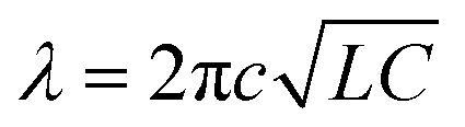 . In which L and C respectively represent the inductance and capacitance in the wave absorber. With the increase of EF, L will decrease, resulting in blue shift of resonance wavelength. At the same time, the resonant wavelength can also be expressed as: λres = α + β × nsp. Where α and β are coefficients closely related to the geometric shape of the model and the surrounding dielectric properties,51,52 and nsp represents the effective refractive index of graphene. Therefore, with the increase of Fermi level, the effective refractive index nsp of graphene SPR decreases, and the resonant wavelength λres decreases, resulting in blue shift. Fig. 6(b) and (c) show the intensity spectra and wavelength shifts of the absorption peaks in the four resonance modes, respectively, during the change of Fermi level. It can be clearly seen that with the increase of the Fermi level, for Mode I, the absorption peak increases first and then decreases. The resonance wavelength shifts from 3239.45 nm blue to 3535.93 nm, with a maximum absorption efficiency of 99.78% at EF = 1.08 eV. The resonance wavelength can be approximately expressed as λI = (−1493.28EF + 4990.65) nm. For mode II, the resonance wavelength shifts from 3371.57 nm blue to 3683.05 nm, and the absorption efficiency is 99.46% at EF = 1.03 eV. The resonance wavelength can be approximately expressed as λII = (−1570.36EF + 5213.11) nm. For mode III, the resonance wavelength shifts from 3544.85 nm blue to 3874.72 nm, with a maximum absorption efficiency of 99.92% at EF = 1.13 eV. The resonance wavelength can be approximately expressed as λIII = (−1663.68EF + 5495.43) nm. For mode IV, the resonance wavelength shifts from 4090.41 nm blue to 4467.51 nm, and the absorption efficiency is 99.91% at EF = 1.13 eV. The resonance wavelength can be approximately expressed as λIV = (−1898.96EF + 6318.31) nm. To sum up, for the four resonance modes, when EF reaches 1.13 eV, the average efficiency of the four absorption peaks is the highest, all of which achieve perfect absorption. Moreover, with the increase of Fermi level, the resonance of SPR will reach the maximum. However, with the continuous increase of EF, the SPR region has reached supersaturation, resulting in a decrease of absorption.53 Therefore, compared with the noble metal absorber, the device can adjust the absorption spectrum by adjusting the Fermi level of the graphene layer, without changing the geometric shape of the absorber, which is more valuable in practical application.