
 Open Access Article
 This Open Access Article is licensed under a Creative Commons Attribution-Non Commercial 3.0 Unported Licence
Exploring a silicene monolayer as a promising sensor platform to detect and capture NO and CO gas†
Duy Khanh Nguyena,
Duc-Quang Hoangb and
D. M. Hoat *cd
*cd
aHigh-Performance Computing Lab (HPC Lab), Information Technology Center, Thu Dau Mot University, Binh Duong Province, Vietnam
bApplied Computational Civil and Structural Engineering Research Group, Faculty of Civil Engineering, Ton Duc Thang University, Ho Chi Minh City, Vietnam
cComputational Laboratory for Advanced Materials and Structures, Advanced Institute of Materials Science, Ton Duc Thang University, Ho Chi Minh City, Vietnam. E-mail: dominhhoat@tdtu.edu.vn
dFaculty of Applied Sciences, Ton Duc Thang University, Ho Chi Minh City, Vietnam
First published on 29th March 2022
Abstract
Searching for new two-dimensional (2D) materials for the early and efficient detection and capture of toxic gas has received special attention from researchers. In this work, we investigate the adsorption of NO and CO molecules onto a silicene monolayer using first-principles calculations. Different numbers of adsorbates, as well as adsorption configurations, have been considered. The results show that up to four NO molecules can be chemically adsorbed onto the pristine monolayer with adsorption energies varying between −0.32 and −1.22 eV per molecule. In these cases, the gas adsorption induces feature-rich electronic behaviors, including magnetic semiconducting and half-metallicity, where the magnetic properties are produced mainly by the adsorbates. Except for two CO molecules adsorbing onto two adjacent Si atoms with an adsorption energy of −0.26 eV per molecule, other adsorption configurations show weak physisorption of CO molecules onto the pristine silicene platform. However, the sensitivity can be enhanced considerably by doping with Al atoms, drastically reducing the adsorption energy to between −0.19 and −0.71 eV per molecule. The doping and adsorption process may lead to either band gap opening or metallization, depending on its configuration. This study reveals the promising applicability of pristine and Al doped silicene monolayers as sensors for more than one single NO and CO molecule.
I. Introduction
Endowed with unprecedented intriguing mechanical and physical properties, graphene and its derivatives have been widely applied in diverse practical fields,1–4 and their success has stimulated significant research efforts to explore more two-dimensional (2D) materials beyond graphene.5–8 Among these, it would be flawed to not mention silicene, an analog of graphene formed by silicon (Si) atoms arranged in hexagonal rings. Early on, Takeda et al.9 theoretically explored the structure of Si and Ge analogs of graphite and discussed the planarity of their respective 2D layers. In contrast to graphene, 2D Si layers show a corrugated stage, which is formed along the perpendicular direction. For the first time, the name “silicene” was given to the silicon-based nanostructures by Gian et al.10 when studying the electronic structure of Si graphene-like sheets using a tight-binding Hamiltonian, where either metals or zero-gap semiconductor natures were obtained. Using first-principles calculations, Cahangirov et al.11 demonstrated a low-buckled structure of silicene with a buckling height of 0.44 Å, which was proven to be stable dynamically and thermally. Interestingly, a Dirac cone is formed by a linear crossing of the π and π* bands at the Fermi level.Despite the early prediction of its outstanding properties, the synthesis of silicene has remained a great challenge, since silicon does not crystallize in a layered structure in nature. One of the first works reporting the epitaxial synthesis of silicene sheets was carried out by Vogt et al.12 The material evidence was provided by scanning tunneling microscopy (STM) and angular-resolved photoemission spectroscopy (ARPES), which matched the theoretical calculations. So far, the synthesis of silicene on different substrates has been investigated both experimentally and theoretically,13–16 and it is an efficient way to either preserve or tune its fundamental properties.17 The successful growth of silicene has opened the door to its applications in nano devices. For example, room temperature silicene-based field-effect transistors (FET) have been fabricated by Tao et al.18 Measurements show a mobility of ∼100 cm2 V−1 s−1. The scalable preparation of freestanding silicene nanosheets has been carried out by Liu et al.19 through a two-step approach: liquid oxidation and exfoliation of a CaSi2 compound. The as-prepared 2D materials exhibit promising applicability as anodes for lithium-ion batteries with a capacity up to 721 mA h g−1 and a cycling stability up to 1800 cycles. In addition, silicene has been also introduced in biodegradable tumor nanomedicine.20
On the other hand, one of the most surprising features of graphene is its capability to adsorb single molecules,21 which suggests that 2D materials are promising platforms to detect toxic gas molecules due to their large-area and active surface.22–24 To date, various research groups have explored monolayer silicene as a gas sensor. For example, Feng et al.25 have investigated gas adsorption on silicene using first-principles calculations. The results confirmed a good sensing capability towards NO2, O2, SO2, NO, and NH2 gases. NO2 adsorption induces a half-metallic nature, while the silicene band gap is opened upon adsorbing the remaining gases. The high reactivity of the silicene monolayer towards nitrogen-based (NH3, NO, and NO2) has been demonstrated by Hu et al.26 via first-principles calculations. The silicene’s band gap can be opened at the Dirac point upon molecular adsorption. Hussain et al.27 have revealed the poor adsorption of CO2, H2S, and SO2 gases onto silicene. However, inducing vacancy defects may lead to a significant enhancement of the gases’ binding to the silicene platform. In addition, doping silicene with N atoms also improves the adsorption of SO2. In contrast, the Al-, B-, and S-doped systems may not show a significant difference in the sensitivity in comparison with that of the pristine one.
Motivated by previous works, we investigate the adsorption of NO and CO molecules on a silicene monolayer using first-principles calculations. It is found that NO gas is chemically adsorbed onto silicene, meanwhile CO gas shows a weak binding. In order to improve the sensitivity towards toxic CO gas, Al-doping is proven to be an efficient approach that drastically reduces the adsorption energy. In addition, the effects of up to four gas molecules on the electronic and magnetic properties of pristine and Al-doped silicene monolayers are also explored in detail. The findings of our work recommend monolayer silicene as a promising platform to detect NO and CO molecules, where more than one molecule could be chemically adsorbed.
II. Computational details
Calculations presented in this work have been carried out using the Vienna ab initio simulation package (VASP), in which the projector-augmented plane (PAW) method is implemented.28,29 Within the framework of the spin-polarized density functional theory (DFT),30,31 the exchange–correlation potential is treated by the Perdew–Burke–Ernzerhof (PBE) generalized gradient approximation.32 A kinetic energy cut-off of 500 eV is set for basis set expansion, while the structural relaxation is determined with residual forces acting on each constituent atom lower than 0.01 eV Å−1. The k-mesh is generated using the Monkhorst–Pack method33 to integrate the Brillouin zone; we use sizes of 10 × 10 × 1 and 20 × 20 × 1 for the structural relaxation and electronic–magnetic properties of the pristine monolayer, respectively. In the cases of doping and molecular adsorption, k-grids of 3 × 3 × 1 and 5 × 5 × 1 are employed, respectively. The interactions between nearby periodic layers are minimized by a vacuum space larger than 14 Å.III. Results and discussion
(A) Pristine silicene monolayer
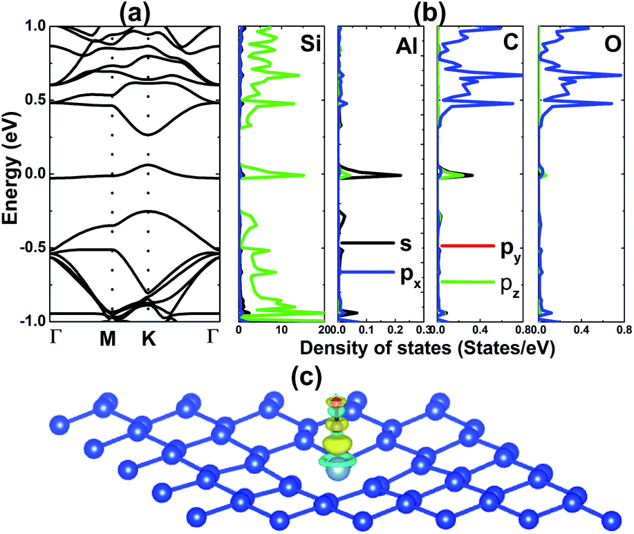
First, the structural and electronic properties of the pristine silicene monolayer are examined. Fig. 1a shows the top view of the optimized structure’s (5 × 5 × 1) supercell. Silicene adopts a low-buckled hexagonal honeycomb arrangement belonging to the P![[3 with combining macron]](https://www.rsc.org/images/entities/char_0033_0304.gif) m1 space group (no. 164). In the equilibrium state, silicene’s structure is characterized by following parameters: (1) a lattice parameter of 3.87 Å, (2) bond length dSi–Si = 2.28 Å, (3) buckling height ΔSi–Si = 0.44 Å and (4) interatomic angle ∠SiSiSi = 116.29°. These results are in good agreement with related works on silicene,34,35 suggesting their reliability. The phonon dispersion curves of the silicene monolayer displayed in Fig. 1b suggest its good dynamical stability, where the out-of-plane mode (ZA) exhibits negligible imaginary frequencies around the zone center (Γ point). The silicene monolayer band structure is illustrated in Fig. 2a. A graphene-like Dirac point at the K point can be seen, indicating the semimetal nature. Corroborating with the projected density of states (PDOS) in Fig. 2b, one can see that the pz state shows a major contribution to the band structure formation around the Fermi level, while the lower part of the valence band and upper part of the conduction band are built mainly by the px–py and s states, respectively. Covalent bonds are characteristic of monoelemental monolayers,34,36 which are formed by shared electrons. In the case of silicene, a large charge accumulation in the bridge region between constituent Si atoms also demonstrates the predominance of the covalent bonds (see the charge density difference illustrated in Fig. 2c, which is defined by Δρ = ρ(monolayer) − ρ(Si1) − ρ(Si2), where the terms on the right side refer to the charge density of the monolayer and each Si atom in the unit cell, respectively).
m1 space group (no. 164). In the equilibrium state, silicene’s structure is characterized by following parameters: (1) a lattice parameter of 3.87 Å, (2) bond length dSi–Si = 2.28 Å, (3) buckling height ΔSi–Si = 0.44 Å and (4) interatomic angle ∠SiSiSi = 116.29°. These results are in good agreement with related works on silicene,34,35 suggesting their reliability. The phonon dispersion curves of the silicene monolayer displayed in Fig. 1b suggest its good dynamical stability, where the out-of-plane mode (ZA) exhibits negligible imaginary frequencies around the zone center (Γ point). The silicene monolayer band structure is illustrated in Fig. 2a. A graphene-like Dirac point at the K point can be seen, indicating the semimetal nature. Corroborating with the projected density of states (PDOS) in Fig. 2b, one can see that the pz state shows a major contribution to the band structure formation around the Fermi level, while the lower part of the valence band and upper part of the conduction band are built mainly by the px–py and s states, respectively. Covalent bonds are characteristic of monoelemental monolayers,34,36 which are formed by shared electrons. In the case of silicene, a large charge accumulation in the bridge region between constituent Si atoms also demonstrates the predominance of the covalent bonds (see the charge density difference illustrated in Fig. 2c, which is defined by Δρ = ρ(monolayer) − ρ(Si1) − ρ(Si2), where the terms on the right side refer to the charge density of the monolayer and each Si atom in the unit cell, respectively).
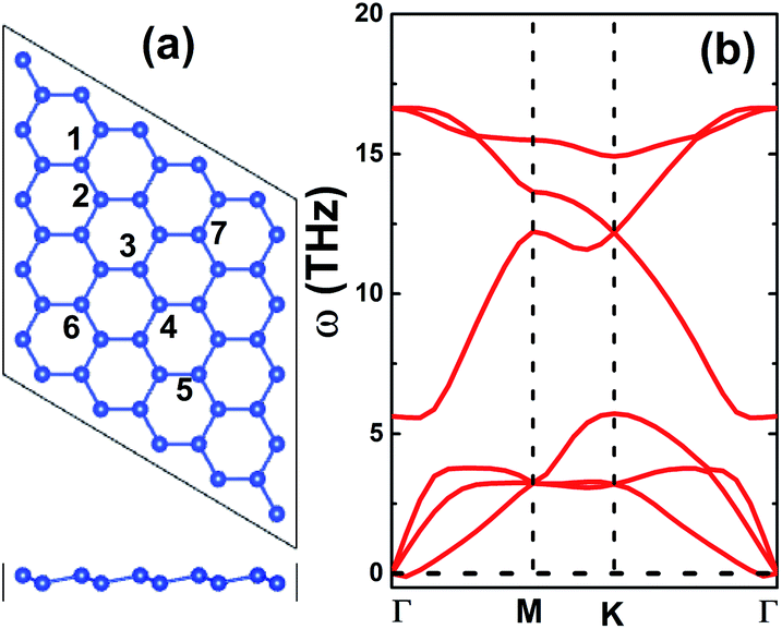 | ||
| Fig. 1 (a) A 5 × 5 × 1 supercell (blue balls: Si) and (b) phonon dispersion curves of the silicene monolayer. | ||
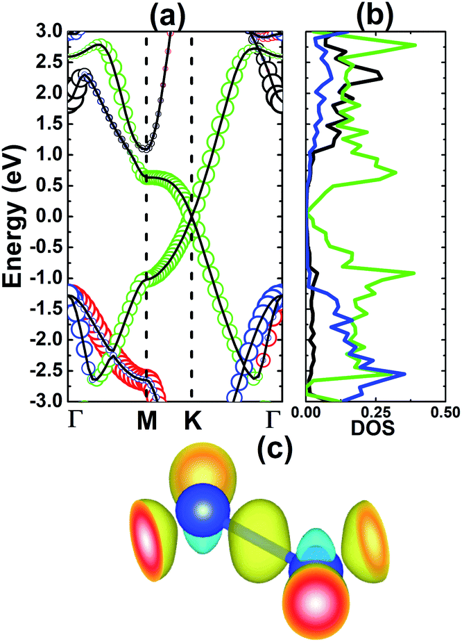 | ||
| Fig. 2 (a) Electronic band structure, (b) projected density of states (DOS – states per eV) (black bubble and line: s state; blue bubble and line: px state; red bubble and line: py state; green bubble and line: pz state) and (c) charge density difference (yellow surface: charge accumulation; blue surface: charge depletion; iso-surface value: 0.01) of the silicene monolayer. | ||
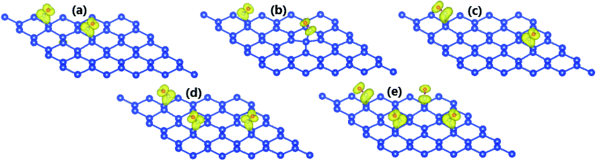
In order to study the adsorption of NO and CO molecules, we use a 5 × 5 × 1 supercell, considering various configurations (the different adsorption and doping sites are indicated in Fig. 1a) as follows:
• One molecule adsorbed, denoted as NO(CO)-adsorbed (NO@ or CO@) silicene, or one Al atom substituted at site 1, denoted as Al-doped silicene (Al–Si).
• Two molecules adsorbed onto sites 1 and 2, denoted as 2NO(CO)1-adsorbed silicene, or two Al atoms substituted at sites 1 and 2, denoted as 2Al1-doped silicene.
• Two molecules adsorbed onto sites 1 and 3, denoted as 2NO(CO)2-adsorbed silicene, or two Al atoms substituted at sites 1 and 3, denoted as 2Al4-doped silicene.
• Two molecules adsorbed onto sites 1 and 4, denoted as 2NO(CO)3-adsorbed silicene, or two Al atoms substituted at sites 1 and 4, denoted as 2Al3-doped silicene.
• Two molecules adsorbed onto sites 1 and 5, denoted as 2NO(CO)4-adsorbed silicene, or two Al atoms substituted at sites 1 and 5, denoted as 2Al4-doped silicene.
• Three molecules adsorbed onto sites 1, 5, and 6, denoted as 3NO(CO)-adsorbed silicene, or three Al atoms substituted at sites 1, 5, and 6, denoted as 3Al-doped silicene.
• Four molecules adsorbed onto sites 1, 5, 6, and 7, denoted as 4NO(CO)-adsorbed silicene, or four Al atoms substituted at sites 1, 5, 6, and 7, denoted as 4Al-doped silicene.
(B) Adsorption of NO molecules onto the silicene monolayer
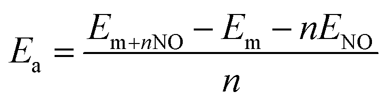
First, we consider the adsorption of one NO molecule onto the silicene monolayer. In the relaxed structure, the molecule bond length dN–O is 1.20 Å, while the distance from molecule to the nearest Si atom dN–Si is 1.99 Å. In order to examine the silicene reactivity towards NO gas, the adsorption energy Ea has been calculated using the following formula:
 | (1) |
According to our calculations, the silicene monolayer is significantly magnetized upon adsorbing NO gas, consistent with previous calculations by Feng et al.25 Fig. 3a exhibits the spin density distribution of the NO-adsorbed system. Note that the magnetic properties are produced mainly by the adsorbed molecules. Specifically, the spin-up states of both N and O atoms are the main contributors to the magnetism with the same magnetic moment of 0.22 (μB). The calculated spin-polarized band structure indicates a band gap opening in both spin channels (see Fig. 3b), however with a strong spin-asymmetry at the vicinity of the Fermi level. To be precise, energy gaps of 0.14 and 0.09 eV have been achieved in the spin-up and spin-down configurations, respectively. These magneto-electronic properties assert the magnetic semiconductor behavior of the silicene monolayer induced by NO gas adsorption. The projected density of states (PDOS) spectra depicted in Fig. 3c clearly show the contributions of the spin-asymmetric N- and O-p orbitals around the Fermi level, which in turn regulate the system’s magnetic and electronic properties. The Si-pz state dominates in the remaining energy ranges, similar to the bare monolayer. Moreover, the charge density difference has also been calculated using the following expression: Δρ = ρ(m + NO) − ρ(m) − ρ(NO), where ρ(m + NO), ρ(m), and ρ(NO) denote the charge density of the gas-adsorbed system, bare monolayer, and NO molecule, respectively. The results, illustrated in Fig. 3d, indicate a large charge accumulation around the NO molecule and also in the N–Si bridge position (with directionality towards the N atom), indicating a charge transfer from the silicene platform to the adsorbed gas.
 | ||
| Fig. 3 (a) Spin density (yellow surface: spin-up; iso-surface value: 0.005), (b) electronic band structure (black line: spin-up; red line: spin-down), (c) projected density of states and (d) charge density difference (yellow surface: charge accumulation; blue surface: charge depletion; iso-surface value: 0.004) of the NO-adsorbed silicene monolayer. | ||
Now, the adsorption of more than one single molecule is explored to clarify its feasibility. By applying eqn (1), the adsorption energies have been calculated, which are given in Table 1. The results suggest that the adsorption of up to four NO adsorbates onto the silicene monolayer is energetically favorable, with Ea varying between −1.22 to −0.32 eV per molecule, where all molecules are chemically adsorbed. Note that the 2NO1@Si system, where two NO molecules are adsorbed onto two adjacent Si atoms, is most stable, exhibiting an Ea which is considerably more negative than those of the other ones. Interestingly, this system is non-magnetic, which can be explained by a short-term strong interaction between Si-pz, N-px(py), and O-px(py). Meanwhile, magnetization is observed mainly in the adsorbates for other systems, as illustrated in Fig. 4, similar to the previous case of single molecule adsorption. In accordance with the magnetic properties, the 2NO1@Si system exhibits a spin-symmetric band structure (Fig. 5a), where the band gap is opened up to 0.03 eV. In the remaining systems, feature-rich properties, including magnetic semiconducting and half-metallicity, can be induced upon managing the number of adsorbates and adsorption configuration, as summarized in Table 2. It is worth mentioning that besides promising silicene applicability towards detecting NO molecules with high sensitivity, the gas-adsorbed systems can be recommended as promising 2D materials for spintronic and optoelectronic applications considering their suitable magneto-electronic properties.
| XO | 2XO1 | 2XO2 | 2XO3 | 2XO4 | 3XO | 4XO | |
|---|---|---|---|---|---|---|---|
| Onto pristine silicene | |||||||
| NO | −0.46 | −1.22 | −0.45 | −0.32 | −0.44 | −0.48 | −0.47 |
| CO | 0.16 | −0.26 | 0.12 | 0.25 | 0.12 | 0.13 | 0.12 |
![[thin space (1/6-em)]](https://www.rsc.org/images/entities/char_2009.gif) |
|||||||
| Onto Al-doped silicene | |||||||
| CO | −0.40 | −0.71 | −0.42 | −0.45 | −0.19 | −0.44 | −0.46 |
 | ||
| Fig. 4 (a) Spin density (yellow surface: spin-up; iso-surface value: 0.005) (a) 2NO2-, (b) 2NO3-, (c) 2NO4-, (d) 3NO-, and (e) 4NO-adsorbed silicene monolayer. | ||
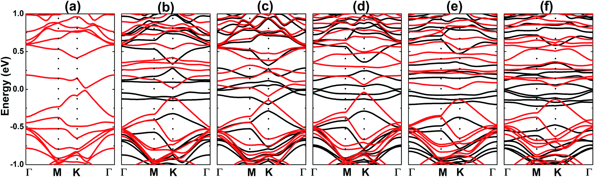 | ||
| Fig. 5 Electronic band structure (black line: spin-up; red line: spin-down) (a) 2NO1-, (b) 2NO2-, (c) 2NO3-, (d) 2NO4-, (e) 3NO- and (f) 4NO-adsorbed silicene monolayer. | ||
| NO | 2NO1 | 2NO2 | 2NO3 | 2NO4 | 3NO | 4NO | |
|---|---|---|---|---|---|---|---|
| Spin-up | 0.14 | 0.03 | 0.13 | M | M | 0.17 | 0.01 |
| Spin-down | 0.09 | 0.03 | 0.14 | M | 0.10 | 0.14 | 0.18 |
| Nature | MS | S | MS | M | HM | MS | MS |
(C) Adsorption of a CO molecule onto pristine and Al-doped silicene monolayers
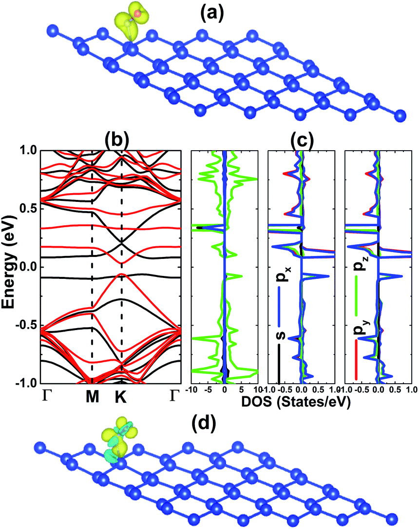
After relaxation, the CO molecule bond length dC–O has the value of 1.16 Å, while the distance from the molecule to the silicene platform dC–Si is 1.89 Å. Using eqn (1) for CO molecules, we obtain an Ea value of 0.16 eV per molecule in the case of one CO adsorbate. The significantly positive Ea suggests that CO gas has been weakly adsorbed onto the silicene monolayer, implying physisorption. This result is in good agreement with previous studies for both silicene nanoribbons38 and monolayers,39 indicating a poor sensing activity towards CO gas. Interestingly, this parameter reduces drastically to a negative value of −0.26 eV per molecule when one more CO molecule is adsorbed onto a neighbouring Si atom, indicating the feasibility of detecting two CO molecules. However, further separating the two adsorbates or increasing the number of adsorbates may worsen the sensitivity, abruptly increasing Ea to positive values of up to 0.25 eV per molecule (see Table 1). It is worth mentioning that the short-term strong interatomic interactions may significantly enhance the gas adsorption. For example, our calculations yield Ea values as small as −1.24 and −0.28 eV per molecule for four NO and CO molecules adsorbed at sites 1, 2, 3, and 4, respectively, which are similar to those of 2XO1-adsorbed systems. Despite weak physisorption, the electronic properties of CO-adsorbed silicene monolayer are given in Fig. 6 for comparison and analysis of the atomic contribution. The platform has not been magnetized under CO adsorption. From panel (a), one can see a significant separation between the valence band maximum point and conduction band minimum point, indicating a band gap opening up to 0.19 eV. The PDOS spectra in panel (b) indicate that in the energy range from −1 to 1 eV, the band structure is formed mainly by the Si-pz state, where a small contribution from CO gas is also observed in the conduction band. The absence of C- and O-px(py) states in the valence band demonstrates a weak interaction with the Si-pz state. Considering the charge density difference between the CO-adsorbed system and the separated bare monolayer and single molecule, which is illustrated in panel (c), we observe the charge accumulation at the C and O sites, and in the region between the C and Si atoms. Meanwhile, charge is depleted mainly around the Si atom, suggesting a charge transfer process from the silicene platform to the gas. In the stable 2CO1 configuration, the band structure profile indicates metallization, provided that the valence band maximum takes place above the Fermi level (see Fig. 7). Readers can find the band structures of other cases in Fig. S1,† where significant energy gaps can be observed.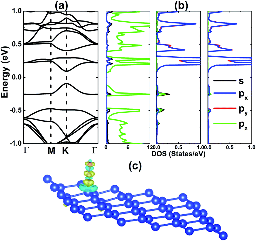 | ||
| Fig. 6 (a) Electronic band structure, (b) projected density of states, and (c) charge density difference (yellow surface: charge accumulation; blue surface: charge depletion; iso-surface value: 0.004) of the CO-adsorbed silicene monolayer. | ||
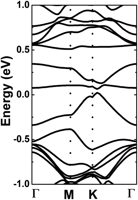 | ||
| Fig. 7 Electronic band structure of the 2CO1-adsorbed silicene monolayer. | ||
It has been demonstrated that the reactivity of 2D materials towards gas molecules can be considerably enhanced by doping.40,41 Herein, we explore the effects of Al doping on the silicene sensitivity towards CO gas. First, the doping energy Ed has been calculated as follows:
 | (2) |
| 1Al | 2Al1 | 2Al2 | 2Al3 | 2Al4 | 3Al | 4Al | |
|---|---|---|---|---|---|---|---|
| Ed | 1.50 | 1.67 | 1.52 | 1.48 | 1.54 | 1.59 | 1.62 |
The adsorption energy Ea of CO gas onto the Al doped silicene monolayer is determined by the following expression:
 | (3) |
Our simulations show that the paramagnetic nature of the doped system is retained upon adsorbing a CO molecule. The band structure and PDOS of the 1CO@Al–Si system are displayed in Fig. 8a and b. A flat energy branch crossing the Fermi level can be noted, giving rise to the metallic nature. This energy curve is formed mainly by Si-pz, Al-s, and C-s states, indicating the s–p hybridization. In the considered energy range, the Al-px(py) states show a significant presence in the lower part of the valence band, meanwhile the gas molecule constituents (C-px(py) and O-px(py)) contribute mainly to the upper part of the conduction band. The charge density difference is illustrated in Fig. 8c, which is defined by: Δρ = ρ(Al + m + CO) − ρ(Al + m) − ρ(CO), where the charge density of the final system, of the doped system without a gas molecule, and of the CO molecule are denoted by the terms on the right side, respectively. Note that the largest charge accumulation is observed in the region between Al and C atoms, while smaller features are present around C and O atoms. In contrast, the charge is depleted around the Al atom, suggesting a charge transfer from the platform to the molecule. Fig. 9 shows the band structures of different cases of doping and adsorption. Depending on the configuration, energy gaps between 0.03 and 0.17 eV are achieved when two single CO molecules are adsorbed. On the contrary, the metallic nature of the doped systems remains unchanged with the presence of three or four adsorbed CO molecules (see Table 4). The results suggest that a two-step process: (1) Al doping, followed by (2) adsorption of CO molecules, may be an efficient way to open the silicene monolayer band gap, besides its promise of detecting and capturing CO gas.
 | ||
| Fig. 8 (a) Electronic band structure, (b) projected density of states, and (c) charge density difference (yellow surface: charge accumulation; blue surface: charge depletion; iso-surface value: 0.004) of the CO-adsorbed Al-doped silicene monolayer. | ||
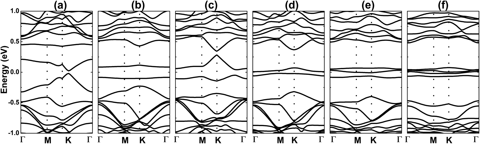 | ||
| Fig. 9 Electronic band structure (black line: spin-up; red line: spin-down) (a) 2CO1-, (b) 2CO2-, (c) 2CO3-, (d) 2CO4-, (e) 3CO- and (f) 4CO-adsorbed Al-doped silicene monolayer. | ||
| 1CO | 2CO1 | 2CO2 | 2CO3 | 2CO4 | 3CO | 4CO | |
|---|---|---|---|---|---|---|---|
| Eg | M | 0.04 | 0.17 | 0.09 | 0.03 | M | M |
IV. Conclusions
In summary, the adsorption of NO and CO molecules onto pristine and Al doped silicene monolayers has been comprehensively explored using first-principles calculations. The pristine monolayer, with a buckled structure, is dynamically stable and electronically a semimetal, whose chemical bonds are predominantly covalent. The adsorption of up to four NO molecules onto the pristine monolayer is stable, showing chemisorption. Apart from the 2NO1@Si system, the platform is significantly magnetized, and the adsorbates are the main contributors to the magnetic properties. Consequently, diverse electronic properties including metallic, semiconductor, magnetic semiconductor, and half-metallic natures are obtained. Two CO molecules can be chemically adsorbed onto two neighboring Si atoms, meanwhile other configurations may be not feasible. Doping with Al atoms has been proven to be efficient to enhance the reactivity of the silicene monolayer towards CO molecules, leading to an abrupt reduction of the adsorption energy. Consequently, CO gas can be efficiently detected and captured. Both Al doping and CO adsorption induces non-magnetic properties in the monolayer, however this two-step process can open the silicene band gap up to 0.17 eV. Our results recommend pristine and Al doped silicene monolayer as promising sensor platforms for more than one single NO and CO molecules. Moreover, with stable chemisorption, the final systems can be used in spintronic and optoelectronic high-performance devices.Conflicts of interest
The authors declare that they have no known competing financial interests or personal relationships that could have appeared to influence the work reported in this paper.Acknowledgements
This research was funded by Foundation for Science and Technology Development of Ton Duc Thang University (FOSTECT), website: http://fostect.tdtu.edu.vn, under grant FOSTECT.2019B.11.References
- K. S. Novoselov, A. K. Geim, S. V. Morozov, D.-e. Jiang, Y. Zhang, S. V. Dubonos, I. V. Grigorieva and A. A. Firsov, Electric field effect in atomically thin carbon films, Science, 2004, 306(5696), 666–669 CrossRef CAS PubMed.
- A. K. Geim and K. S. Novoselov, The rise of graphene, in Nanoscience and technology: a collection of reviews from nature journals, World Scientific, 2010, pp. 11–19 Search PubMed.
- X. J. Lee, B. Y. Z. Hiew, K. C. Lai, L. Y. Lee, S. Gan, S. Thangalazhy-Gopakumar and S. Rigby, Review on graphene and its derivatives: synthesis methods and potential industrial implementation, J. Taiwan Inst. Chem. Eng., 2019, 98, 163–180 CrossRef CAS.
- D. Chen, H. Zhang, Y. Liu and J. Li, Graphene and its derivatives for the development of solar cells, photoelectrochemical, and photocatalytic applications, Energy Environ. Sci., 2013, 6(5), 1362–1387 RSC.
- S. Z. Butler, S. M. Hollen, L. Cao, Y. Cui, J. A. Gupta, H. R. Gutiérrez, T. F. Heinz, S. S. Hong, J. Huang and A. F. Ismach, et al., Progress, challenges, and opportunities in two-dimensional materials beyond graphene, ACS Nano, 2013, 7(4), 2898–2926 CrossRef CAS PubMed.
- G. R. Bhimanapati, Z. Lin, V. Meunier, Y. Jung, J. Cha, S. Das, D. Xiao, Y. Son, M. S. Strano and V. R. Cooper, et al., Recent advances in two-dimensional materials beyond graphene, ACS Nano, 2015, 9(12), 11509–11539 CrossRef CAS PubMed.
- J. Di, J. Xia, H. Li and Z. Liu, Freestanding atomically-thin two-dimensional materials beyond graphene meeting photocatalysis: opportunities and challenges, Nano Energy, 2017, 35, 79–91 CrossRef CAS.
- Y. Zhang, A. Rubio and G. Le Lay, Emergent elemental two-dimensional materials beyond graphene, J. Phys. D: Appl. Phys., 2017, 50(5), 053004 CrossRef.
- K. Takeda and K. Shiraishi, Theoretical possibility of stage corrugation in Si and Ge analogs of graphite, Phys. Rev. B: Condens. Matter Mater. Phys., 1994, 50(20), 14916 CrossRef CAS PubMed.
- G. G. Guzmán-Verri and L. L. Y. Voon, Electronic structure of silicon-based nanostructures, Phys. Rev. B: Condens. Matter Mater. Phys., 2007, 76(7), 075131 CrossRef.
- S. Cahangirov, M. Topsakal, E. Aktürk, H. Şahin and S. Ciraci, Two-and one-dimensional honeycomb structures of silicon and germanium, Phys. Rev. Lett., 2009, 102(23), 236804 CrossRef CAS PubMed.
- P. Vogt, P. De Padova, C. Quaresima, J. Avila, E. Frantzeskakis, M. C. Asensio, A. Resta, B. Ealet and G. Le Lay, Silicene: compelling experimental evidence for graphenelike two-dimensional silicon, Phys. Rev. Lett., 2012, 108(15), 155501 CrossRef PubMed.
- N. W. Johnson, P. Vogt, A. Resta, P. De Padova, I. Perez, D. Muir, E. Z. Kurmaev, G. Le Lay and A. Moewes, The metallic nature of epitaxial silicene monolayers on Ag (111), Adv. Funct. Mater., 2014, 24(33), 5253–5259 CrossRef CAS.
- Z.-L. Liu, M.-X. Wang, J.-P. Xu, J.-F. Ge, G. Le Lay, P. Vogt, D. Qian, C.-L. Gao, C. Liu and J.-F. Jia, Various atomic structures of monolayer silicene fabricated on Ag (111), New J. Phys., 2014, 16(7), 075006 CrossRef CAS.
- P. De Padova, H. Feng, J. Zhuang, Z. Li, A. Generosi, B. Paci, C. Ottaviani, C. Quaresima, B. Olivieri and M. Krawiec, et al., Synthesis of multilayer silicene on Si (111) √3 × √3-Ag, J. Phys. Chem. C, 2017, 121(48), 27182–27190 CrossRef CAS.
- B. Lalmi, H. Oughaddou, H. Enriquez, A. Kara, S. Vizzini, B. Ealet and B. Aufray, Epitaxial growth of a silicene sheet, Appl. Phys. Lett., 2010, 97(22), 223109 CrossRef.
- H. Liu, J. Gao and J. Zhao, Silicene on substrates: a way to preserve or tune its electronic properties, J. Phys. Chem. C, 2013, 117(20), 10353–10359 CrossRef CAS.
- L. Tao, E. Cinquanta, D. Chiappe, C. Grazianetti, M. Fanciulli, M. Dubey, A. Molle and D. Akinwande, Silicene field-effect transistors operating at room temperature, Nat. Nanotechnol., 2015, 10(3), 227–231 CrossRef CAS PubMed.
- J. Liu, Y. Yang, P. Lyu, P. Nachtigall and Y. Xu, Few-layer silicene nanosheets with superior lithium-storage properties, Adv. Mater., 2018, 30(26), 1800838 CrossRef PubMed.
- H. Lin, W. Qiu, J. Liu, L. Yu, S. Gao, H. Yao, Y. Chen and J. Shi, Silicene: wet-chemical exfoliation synthesis and biodegradable tumor nanomedicine, Adv. Mater., 2019, 31(37), 1903013 CrossRef PubMed.
- F. Schedin, A. K. Geim, S. V. Morozov, E. Hill, P. Blake, M. Katsnelson and K. S. Novoselov, Detection of individual gas molecules adsorbed on graphene, Nat. Mater., 2007, 6(9), 652–655 CrossRef CAS PubMed.
- S. Yang, C. Jiang and S.-h. Wei, Gas sensing in 2D materials, Appl. Phys. Rev., 2017, 4(2), 021304 Search PubMed.
- C. Anichini, W. Czepa, D. Pakulski, A. Aliprandi, A. Ciesielski and P. Samorì, Chemical sensing with 2D materials, Chem. Soc. Rev., 2018, 47(13), 4860–4908 RSC.
- M. Donarelli and L. Ottaviano, 2D materials for gas sensing applications: a review on graphene oxide, MoS2, WS2 and phosphorene, Sensors, 2018, 18(11), 3638 CrossRef PubMed.
- J.-w. Feng, Y.-j. Liu, H.-x. Wang, J.-x. Zhao, Q.-h. Cai and X.-z. Wang, Gas adsorption on silicene: a theoretical study, Comput. Mater. Sci., 2014, 87, 218–226 CrossRef CAS.
- W. Hu, N. Xia, X. Wu, Z. Li and J. Yang, Silicene as a highly sensitive molecule sensor for NH3, NO and NO2, Phys. Chem. Chem. Phys., 2014, 16(15), 6957–6962 RSC.
- T. Hussain, T. Kaewmaraya, S. Chakraborty and R. Ahuja, Defect and substitution-induced silicene sensor to probe toxic gases, J. Phys. Chem. C, 2016, 120(44), 25256–25262 CrossRef CAS.
- G. Kresse and J. Furthmüller, Efficiency of ab-initio total energy calculations for metals and semiconductors using a plane-wave basis set, Comput. Mater. Sci., 1996, 6(1), 15–50 CrossRef CAS.
- G. Kresse and J. Furthmüller, Efficient iterative schemes for ab initio total-energy calculations using a plane-wave basis set, Phys. Rev. B: Condens. Matter Mater. Phys., 1996, 54(16), 11169 CrossRef CAS PubMed.
- P. Hohenberg and W. Kohn, Inhomogeneous electron gas, Phys. Rev. B: Solid State, 1964, 136(3), B864 CrossRef.
- W. Kohn and L. J. Sham, Self-consistent equations including exchange and correlation effects, Phys. Rev., 1965, 140(4), A1133 CrossRef.
- J. P. Perdew, K. Burke and M. Ernzerhof, Generalized gradient approximation made simple, Phys. Rev. Lett., 1996, 77(18), 3865 CrossRef CAS PubMed.
- H. J. Monkhorst and J. D. Pack, Special points for Brillouin-zone integrations, Phys. Rev. B: Solid State, 1976, 13(12), 5188 CrossRef.
- H. Şahin, S. Cahangirov, M. Topsakal, E. Bekaroglu, E. Akturk, R. T. Senger and S. Ciraci, Monolayer honeycomb structures of group-IV elements and III–V binary compounds: first-principles calculations, Phys. Rev. B: Condens. Matter Mater. Phys., 2009, 80(15), 155453 CrossRef.
- B. van den Broek, M. Houssa, E. Scalise, G. Pourtois, V. Afanas’ev and A. Stesmans, First-principles electronic functionalization of silicene and germanene by adatom chemisorption, Appl. Surf. Sci., 2014, 291, 104–108 CrossRef CAS.
- P. Yuan, T. Zhang, J. Sun, L. Liu, Y. Yao and Y. Wang, Recent progress in 2D group-V elemental monolayers: fabrications and properties, J. Semicond., 2020, 41(8), 081003 CrossRef CAS.
- G. K. Walia, D. K. K. Randhawa and K. S. Malhi, Rise of silicene and its applications in gas sensing, J. Mol. Model., 2021, 27(10), 1–11 CrossRef PubMed.
- T. H. Osborn and A. A. Farajian, Silicene nanoribbons as carbon monoxide nanosensors with molecular resolution, Nano Res., 2014, 7(7), 945–952 CrossRef CAS.
- J. Prasongkit, R. G. Amorim, S. Chakraborty, R. Ahuja, R. H. Scheicher and V. Amornkitbamrung, Highly sensitive and selective gas detection based on silicene, J.Phys. Chem. C, 2015, 119(29), 16934–16940 CrossRef CAS.
- K. Ding, Y. Lin and M. Huang, The enhancement of NO detection by doping strategies on monolayer MoS2, Vacuum, 2016, 130, 146–153 CrossRef CAS.
- M. J. Szary, MoS2 doping for enhanced H2S detection, Appl. Surf. Sci., 2021, 547, 149026 CrossRef CAS.
- A. Patra, H. Peng, J. Sun and J. P. Perdew, Rethinking CO adsorption on transition-metal surfaces: effect of density-driven self-interaction errors, Phys. Rev. B, 2019, 100(3), 035442 CrossRef CAS.
Footnote |
| † Electronic supplementary information (ESI) available. See DOI: 10.1039/d2ra00442a |
| This journal is © The Royal Society of Chemistry 2022 |