
 Open Access Article
 This Open Access Article is licensed under a Creative Commons Attribution-Non Commercial 3.0 Unported Licence
Application of a dual functional blocking layer for improvement of the responsivity in a self-powered UV photodetector based on TiO2 nanotubes†
Alireza Zarea,
Saeed Behaeinb,
Mahmoud Moradib and
Zahra Hosseini *a
*a
aFaculty of Advanced Technologies, Shiraz University, P.O. Box: 7194684560, Shiraz, Iran. E-mail: zahrahosseini@shirazu.ac.ir
bPhysics Department, School of Science, Shiraz University, Shiraz, Iran
First published on 29th March 2022
Abstract
A layer of graphene quantum dots (GQDs) was applied on the photoanode of a self-powered photoelectrochemical (PEC) UV photodetector based on TiO2 nanotubes (NTs). The GQDs layer acted as a dual functional layer and improved the photodetector performance by both UV light absorption and blocking the charge carriers recombination at the photoanode/electrolyte interface. The short circuit current density (Jsc) and thereby the responsivity of the PEC UV photodetector was enhanced by 473%. The highest value of the responsivity in this work obtained for the PEC UV photodetector with the dual functional GQDs layer was as much as 42.5 mA W−1. This value is far better than previously reported responsivities of the PEC devices based on TiO2 NTs as a photoanode. This high responsivity was obtained under the illumination of a very low intensity UV light (365 nm, 2 mW cm−2) and 0 V bias. Moreover, the sensitivity of the PEC UV photodetector with the dual functional GQDs layer has been improved by 345%, which is almost 3.5 times higher compared to the sensitivity of its counterpart without the GQDs coating. The devices with the dual functional GQDs layer present a splendid repeatability and stability. The rise time and the decay time of this device were measured to be 0.73 s and 0.88 s under the on/off switching UV LEDs, respectively. The electrochemical impedance spectroscopy (EIS) results prove the role of the GQDs layer as an effective blocking layer on the photoanode, hindering the charge carrier recombination at the photoanode/electrolyte interface. This study shows that application of the dual functional GQDs layer in the PEC UV photodetector based on TiO2 NTs is an effective approach for improving the responsivity and sensitivity of a self-powered PEC UV PD, which brought us the possibility of detecting low UV index radiation and using the self-powered photodetectors in cutting-edge wearable electronic devices for the aim of health, safety and environmental monitoring.
Introduction
The process of detecting ultraviolet (UV) light has always been critical in scientific applications and several industries such as UV communication, environmental monitoring, biomedical and chemical analysis.1–4 Recently, optoelectronic wearable devices with the intentions of health, safety and environmental monitoring are becoming more and more popular. Thus, a device with the capability of working without any external bias voltage, namely a self-powered photodetector and the ability of detecting low intensity UV light as well, is essential. So far, several types of self-powered photodetectors have been developed. Xu et al. reported a self-powered UV photodetector based on p-CuZnS/n-TiO2.5 Although it was designed to operate at 0 V bias for the aim of a wearable UV detection system, the responsivity of the device was rather low. Gao et al. developed a self-powered p–n heterojunction UV photodetector using nanorod arrays.6 The device worked in a self-powered mode but still suffered from an insufficient photocurrent and thereby low responsivity. Another type of self-powered UV photodetector based on a p–n junction was revealed by Ning et al. which showed a very low responsivity of 1 mA W−1 at zero bias.7 Despite the great diversity of developed self-powered UV photodetectors, still innovative and simple approaches need to be developed to improve the spectral responsivity of these devices as well as reducing the cost and fabrication difficulties. Among various types of self-powered UV photodetectors, photoelectrochemical (PEC) cells are of great interest owing to their ease of fabrication process and low cost.8 Up to this point, several wide bandgap semiconductors including ZnO, SnO2, TiO2, etc., have been utilized in the PEC UV photodetectors.9–11 The investigations confirm TiO2 as an ideal candidate for the main UV absorption material in the PEC UV photodetectors and photocatalyst applications12–14 due to their appropriate characteristics such as: wide bandgap, Eg (anatase phase) = 3.2 eV, superior chemical stability, no toxicity and environmental safety.15–17 TiO2 has been applied in PEC UV photodetectors in different structures,18–20 among which, TiO2 nanotube has gained much attention due to high surface area, proper charge carrier transport and inexpensive method of synthesis.21–23 Li et al. manufactured a self-powered ultraviolet photodetector based on TiO2/Ag/ZnS nanotubes with the maximum photocurrent of 497 μA under UV illumination of 40 mW cm−2 and 0 V bias.24 Chen et al. reported a self-powered UV photodetector with self-doping TiO2 nanotube arrays which has gained the maximum photo responsivity of 22 mA W−1.25 Li et al. prepared a TiO2–graphene composite as the UV sensitive layer in a self-powered UV photodetector, which has the ability to reach the responsivity of 11 μA W−1.26In the PEC UV photodetectors based on TiO2 NTs, the tubes are responsible for UV light absorption. A full absorption of incident UV photons is necessary in a competent UV photodetector. Short TiO2 NTs are not able to absorb UV photons efficiently. Therefore, application of long TiO2 NTs seems to be essential for achieving enough light absorption and thereby obtaining high current and responsivity in the device. On the other hand, research shows that fabrication of defect free and long TiO2 NTs is challenging.27 Due to the longer TiO2 NTs, the carrier transport path length is relatively longer and consequently the probability of emerging defects on their surface is much higher. Chances of electron–hole recombination are thus higher in longer TiO2 NTs. In fact, there is usually a trade-off between light harvesting efficiency and carrier collection efficiency in the devices based on the TiO2 NTs. One should use the shortest possible TiO2 NTs to maximize the electron collection efficiency. This can be the reason that despite all the outstanding properties of TiO2 nanotubes, low photo response and quantum efficiency limit the associated photodetectors' practical use in innovative optoelectronic devices.10 Therefore, new practical strategies need to be applied to improve the responsivity of these devices.
Herein, we introduce a unique idea of applying graphene quantum dots (GQDs) to the self-powered PEC UV photodetector based on TiO2 NTs as a dual functional coating. A monolayer of GQDs which serves as both a light absorber and a blocking layer was used in the device. GQDs are size-dependent bandgap semiconductors with high carrier mobility and good chemical stability which have been used as the photo-sensitive material in different photoelectrochemical and photocatalytic applications.28–30 The studies show that the relative position of the GQDs and TiO2 energy levels guarantees the injection of the electrons from the conduction band (CB) of GQDs to the CB of TiO2. Therefore, in our PEC UV photodetectors, there are two active UV absorbing layer, i.e., TiO2 and GQDs. The photogenerated electrons in the GQDs finally contribute in the current generation by getting injected into the CB of TiO2 NTs and transferring to the external circuit. The GQDs also cover the surface defects of the TiO2 NTs and block the recombination of the photogenerated electrons with the redox species in the electrolyte. Accordingly, our results show that compared to the photodetectors made with bare TiO2 NTs, the device with GQDs reveals improved responsivity and sensitivity. What's more, our approach lets us skip the challenges of fabricating defect free, long TiO2 NTs and provides the opportunity to make self-powered PEC UV photodetectors with high responsivity using shorter TiO2 NTs. Considering the remarkable improvements achieved in the performance of the self-powered photodetectors based on TiO2 NTs, employing a proper blocking layer which also serves as a UV absorber layer is an effective practical procedure to develop the performance of the self-powered PEC UV photodetectors based on TiO2 NTs.
Experimental
Synthesis of TiO2 nanotubes (NTs)
TiO2 NTs were synthesized on Ti foil via a two-step anodization method. 0.25 mm thick titanium foil (99.7%; Sigma-Aldrich) with desired dimension were sonicated in ethanol, acetone and DI water to remove any unwanted substance on the surface of the Ti foil. A two-electrode electrochemical cell filled with electrolyte containing ethylene glycol solution of 0.3 wt% NH4F and 2 vol% H2O was used for the preparation of NTs on Ti foil. The Pt and Ti were used as counter and working electrodes respectively. The first anodization step was done for 30 minutes under 60 V potential and 25 °C temperature. To obtain a highly ordered TiO2 NTs, the first layer of NTs was peeled off the foil via sonication of the sample in DI water for 10 minutes. The second anodization step was performed in a new electrolyte solution at different times to get the desired NTs with different heights from approximately 3 to 20 μm. To attain the TiO2 NTs in anatase phase, an annealing process of anodized samples was carried out in 450 °C for 2 h.Synthesis of GQDs
Hydrothermal method was used to prepare N-doped GQDs as it was reported in our previous work.31 A mixture of 1.26 g citric acid monohydrate (Merck), 1.08 urea (Merck) and 30 mL H2O were stirred to get a fully clear solution. The prepared solution was then transferred into a 50 mL Teflon lined autoclave and heated in an electric furnace in 200 °C for 24 h. After the heating step, the final yellow solution was centrifuged at 6000 rpm for 20 minutes. In the final step, the separated GQDs powder was re-dispersed into DI water.Assembly of PEC UV photodetector
Fluorine doped tin oxide (FTO)-coated transparent glass was used as counter electrode in the device. Platinized counter electrode was prepared by depositing Pt paste (Sharif Solar, Iran) onto the surface of the FTO glass using Dr Blade method. For the application of the blocking layer, the GQDs coated on the TiO2 NTs by dip coating the NTs in GQDs solution for a specific time. Subsequently, the platinized FTO glass and the photoanode were sealed (with Surlyn spacer) with conductive side of the FTO facing inward. Finally, some I/I3− redox couple electrolyte (Sharif Solar, Iran) was injected into the space between two electrodes for providing ionic conductivity. The photodetectors made with and without GQDs blocking coating are labelled as GQD-TNT-PD and TNT-PD, respectively.Characterization
The X-ray diffraction spectroscopy (XRD; D8-ADVANCE) with Cu k (1/4 1.540 Å) radiation over Bragg angles ranging from 10° to 80° was performed to confirm the crystal structure of GQDs and TiO2 NTs. The GQDs morphology was inspected using transmission electron microscope (TEM; Zeiss EM900). The surface morphology of TiO2 NTs was analysed using field emission scanning electron microscope (FESEM; MIRA3 TESCAN-XMU) and scanning electron microscope (SEM; TESCAN-Vega3) equipped with an energy-dispersive X-ray spectrometer (EDS) for elemental analysis. To characterize the functional groups on the surface of GQDs, a Fourier-transform infrared spectroscopy (FTIR; Tensor II, Bruker) was conducted. Raman spectroscopy (Raman; LabRam HR, Horiba) was used to verify the coverage of GQDs on the surface of TiO2 NTs. The optical transmittance and absorbance of GQDs were analysed using UV-Vis dual-beam spectrophotometer (UV-1280). The photoluminescence spectroscopy (PL) of GQDs is carried out by Agilent G9800A. UV-Vis diffused reflectance spectroscopy (DRS) was performed to confirm the absorbing performance of GQDs by Avantes-Avaspec-2048 device. HITACHI 8WF8T5, 365 nm was used as the UV light source. 360 nanometre wavelength light emitting diodes were used as the switching UV source. All the photocurrent measurements and EIS spectroscopy were done by an Auto Lab electrochemical workstation (AUTO LAB PGSTAT302N) and Keithley Ampere meter 6487.Results and discussion
The yellow aqueous GQDs solution, which is the final product of previously described hydrothermal process, was analysed with TEM to determine the shape and size of the GQDs. As it is shown in Fig. 1a the GQDs are spherical particles with sizes less than 20 nm. The XRD pattern of the aqueous GQDs solution is demonstrated in ESI, Fig. S1.† A broad diffraction peak at around 2θ = 25° is obvious which is corresponding to (002) crystal phase of graphite. Another broad peak at about 2θ = 9° which is attributed to the (001) plane of graphitic nitride carbon can be seen in Fig. S1†.32,33 The absorption ability of the GQDs in UV region was examined with optical absorbance spectra. Fig. 1b illustrates a broad absorption band in the UV region with a peak at about 320 nm for the GQDs. The broad and intense spectral absorption of the GQDs in the UV region confirms that the GQDs can serve as UV absorbing material in the UV photodetector. The PL spectra of the GQDs is exhibited in Fig. S2.† The PL property of the GQDs guarantees the electron transfer to the neighboring TiO2 NTs rather than thermal relaxation. To determine the functional groups on the surface of the GQDs, FTIR spectroscopy was utilized and the obtained spectrum is shown in Fig. 1c. The absorption bands at 3515 and 3055 cm−1 describe the O–H stretching vibrations. The wavenumbers at 2880 cm−1, 1610 cm−1 and 1464 cm−1 suggests C–H, C![[double bond, length as m-dash]](https://www.rsc.org/images/entities/char_e001.gif) O and CC stretching vibrations in carboxyl group. The other distinct absorption bands are 1361 cm−1 related to C–N in-plane bending, 1084 cm−1 ascribed to the C–O bending vibrations and 843 cm−1 attributed to the C–H out of plane vibrations. The numerous number of carbonyl, carboxyl and hydroxyl groups on the surface of GQDs, facilitates the adsorption of GQDs on the surface of the TiO2 NTs.32–34
O and CC stretching vibrations in carboxyl group. The other distinct absorption bands are 1361 cm−1 related to C–N in-plane bending, 1084 cm−1 ascribed to the C–O bending vibrations and 843 cm−1 attributed to the C–H out of plane vibrations. The numerous number of carbonyl, carboxyl and hydroxyl groups on the surface of GQDs, facilitates the adsorption of GQDs on the surface of the TiO2 NTs.32–34
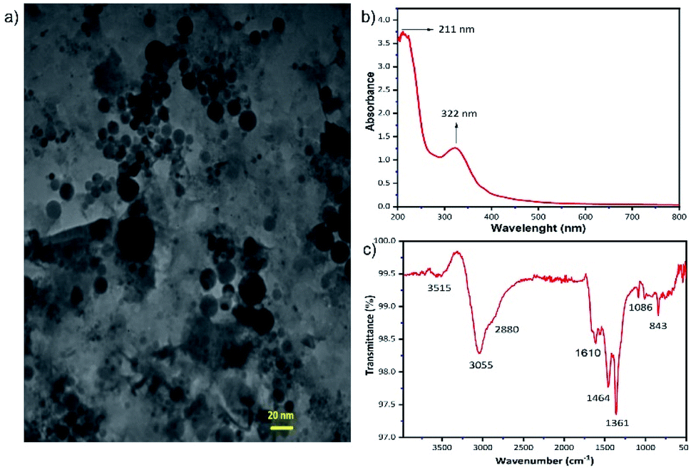 | ||
| Fig. 1 (a) TEM image, (b) UV-Vis absorption spectrum, and (c) FTIR spectrum of the GQDs. | ||
Fig. 2a typically shows the cross sectional FESEM image of the TiO2 NTs prepared by anodization process at 60 V for 45 min. It is clear that highly ordered, closely and firmly packed tubes were obtained which create defect free paths for electrons. Fig. 2b shows the top-view of the NTs indicating a smooth top surface with average tube diameter of 100–130 nm and of course a great sublayer for the attachment of the GQDs. The SEM images of the TiO2 NTs in different lengths and full information about the anodization parameters are provided in Fig. S3 and Table S1.† Additionally, XRD spectrum (Fig. S4†) confirms the crystalline structure of the TiO2 NTs with anatase phase. Existing diffraction peaks [215], [120], [204], [211], [105], [200], [112], [004] and [101] of Fig. S4† are all indexed to anatase phase of TiO2 (JCPDS card #41-2127).35 Coating the TiO2 NTs with the GQDs was performed by the immersion of the TiO2 NTs photoanode in the GQDs solution for a specific time. Fig. 2c shows the structural morphology of the TiO2 NTs coated with the GQDs. The presence of the GQDs on the surface of the TiO2 NTs is obvious and there is no change in the structural morphology of the TiO2 NTs after the GQDs coating. The energy-dispersive X-ray spectroscopy (EDS mapping) was used for elemental characterization of the GQDs coated TiO2 NTs. The EDS mapping picture of C element (Fig. 2d) proves complete loading and uniform coverage of the TiO2 NTs surface with the GQDs. The inset of Fig. 2d shows the EDS mapping picture of C element on the pure TiO2 NTs. The C element which is present on the surface of the uncoated TiO2 NTs is from the environmental pollution and its concentration on the TiO2 NTs surface is significantly low compared to the C element concentration of the TiO2 NTs surface after the GQDs coating.
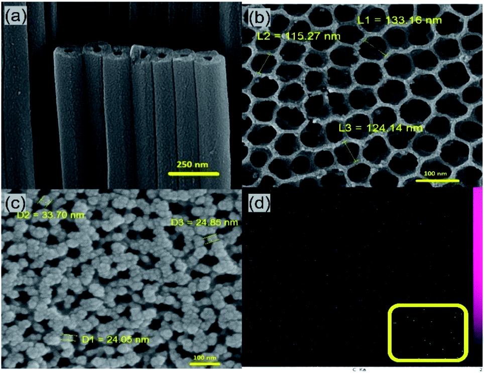 | ||
| Fig. 2 (a) Cross-sectional FESEM image of the TiO2 NTs, (b) top-view FESEM image of the TiO2 NTs, (c) top-view FESEM image of the GQDs coated TiO2 NTs, and (d) EDS mapping image of C element on the GQDs coated TiO2 NTs. The inset shows the EDS mapping image of C element on the pure TiO2 NTs. The NTs are prepared by anodization at 60 V for 45 minutes. | ||
The Raman spectra of the pure TiO2 NTs and the GQDs coated TiO2 NTs are compared in Fig. 3a. According to the symmetry group analysis, a few clear characteristic peaks can be seen centered at 144 cm−1, 369 cm−1, 515 cm−1 and 637 cm−1 which are denoted to the active modes of the pure anatase TiO2. Yet, two more peaks shown in Fig. 3a inset, centred at 1386 cm−1 and 1537 cm−1 in the spectra of the GQDs coated TiO2 NTs, are related to the active Raman modes of the GQDs and again a verification of the GQDs coverage on the NTs sample.36
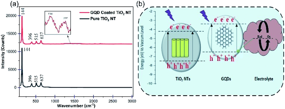 | ||
| Fig. 3 (a) Raman spectra of the TiO2 NTs photoanode before and after decorating with the GQDs. (b) Energy band diagram schematic of the PEC UV photodetector based on the GQDs coated TiO2 NTs. | ||
Despite the fact that the TiO2 NTs serve as an efficient UV light absorber, here the decorating GQDs on the NTs surface are also accountable material which absorb UV photons. The relative position of the energy levels for the different parts of the photodetector is demonstrated in Fig. 3b. When the device is exposed to UV radiation, the UV photons will be absorbed by both TiO2 NTs and the GQDs and excite the electrons to the corresponding CBs. According to Fig. 3b, the existed electrons in the CB of GQDs will be injected into the CB of the TiO2 NTs due to the lower energy band of the NTs compared to the GQDs. The injected electrons along with the photogenerated electrons in the TiO2 NTs, contribute to the current flow by traveling through the NTs and the external circuit, until they reach the counter electrode. Transferring of electrons from the counter electrode to the electrolyte and the regeneration of the GQDs happens through electrolyte oxidation and reduction activities.
For the purpose of achieving the best photo current and photo responsivity together with fast response, optimization of the TiO2 NTs height and also the GQDs loading time on the NTs surface has been done. In the very first step, a few numbers of the PEC UV photodetectors with bare TiO2 NTs as photoanode and also different tube height from 3 to 20 nm were assembled and their detecting performance under UV illumination of 365 nm and 2 mW cm−2 power intensity was examined. The SEM image of different TiO2 NTs are exhibited in Fig. S3.† It is clear that the TiO2 NTs are ordered well on the Ti foil through the anodization process and the NTs length has been increased by increasing the anodization time. According to Fig. S5 and Table S2,† the maximum photo responsivity of 13.5 mA W−1 achieved by application of approximately 15 μm long TiO2 NTs in photoanode of the PEC UV photodetector.
As it is shown in Table S2,† gradual increase in tube length resulted in an increase in the photocurrent density and thereby the photo responsivity. Excessive increase in tube length longer than 15 μm will cause a decrease in the photocurrent. This can be attributed to the longer electron path length which increases the chance of electron–hole recombination before the injection of electrons to the FTO. In order to figuring out the appropriate time for the GQDs loading on the NTs surface, several numbers of photoanode with 7.5 and 15 μm long TiO2 NTs were synthesized and immersed in the GQDs solution. A variety of PEC UV photodetectors were assembled using GQDs coated photoanodes with different immersion time intervals. Their detecting performance were analysed under UV light (365 nm, 2 mW cm−2). As demonstrated in Fig. S6 and Table S3,† the optimum time for the GQDs loading on 7.5 μm long NTs is 9 days. As a matter of fact, longer loading time of the GQDs on the NTs surface will bring about the higher amounts of GQDs adsorbed on the NTs surface which resulted in an increment of the UV photons absorption and thereby higher photocurrent generation in the device. Extending immersion time more than 9 days results in a decrease in the photocurrent and deteriorates the detecting performance. The decrease in the photocurrent is due to the excessive accumulation of the GQDs on the NTs surface. In this condition, electrons are more likely to be trapped in the thick layer of the GQDs and also the chance of recombination is greater. We did the same experiments with 15 μm long NTs, up to 20 days, in order to find the optimum immersion time for the GQDs loading. The results (Fig. S7†) show that long NTs need a very long time for the GQDs coating. But we did not perform the experiments for longer times as we believe such long loading time is not practical from industrial point of view.
Fig. 4a, b and Table 1 show the photocurrent of TNT-PD and GQD-TNT-PD devices, in both dark and under illumination condition (365 nm, 2 mW cm−2). As it is shown in Table 1, the TNT-PD or GQD-TNT-PD devices with 15 μm long NTs have higher photocurrent compared to their counterparts made with 7.5 μm long NTs. Longer NTs provide higher surface area for the UV light absorption or the GQDs adsorption compared to the shorter ones, which results in higher responsivity in both TNT-PD and GQD-TNT-PD devices. Before coating the TiO2 NTs with the GQDs, the photo responsivity of the 15 μm TNT-PD device is around 111% higher than the photo responsivity of the 7.5 μm TNT-PD device. With the application of the dual functional blocking layer, the photocurrent density in the photodetectors made with 7.5 and 15 μm long NTs increased by 473% and 348% respectively. Therefore, the difference between the photo responsivity of devices made with 7.5 and 15 μm long NTs decreases to 56% after application of the GQDs coating. The increase in the photocurrent after the application of the GQDs can be attributed to the higher light harvesting in both devices. When using GQDs, both TiO2 NTs and the GQDs contribute in the light absorption. Therefore, the electron–hole generation is higher when using the GQDs in the device. We compared the diffuse reflection spectra (DRS) of two photoanodes, with and without the GQDs. The spectra shown in Fig. S8,† indicate that no more light scattering happens when using the GQDs coating on the TiO2 NTs. Thus, light trapping cannot be the cause for the increased photocurrent of devices with GQD. Moreover, by application of the GQDs coating, the photo sensitivity of the PEC UV photodetectors increased by 345.7% and 171.2% when using 7.5 and 15 μm TiO2 NTs in the device, respectively. Although a higher amount of photocurrent has been achieved by application of 15 μm NTs in the photoanode, the percentage of photo sensitivity increment is relatively low. This can be ascribed to the higher dark current in the PEC UV photodetector made by the 15 μm NTs. In the anodization process for the preparation of longer TiO2 NTs, the upper parts of the tubes remain in the fluoride-containing electrolyte for longer times. Therefore, chances of chemical etching and formation of holes and defects on the surface of NTs increases.27 Thus, the PEC UV photodetector made by the 15 μm NTs have higher dark currents and thereby lower sensitivity.
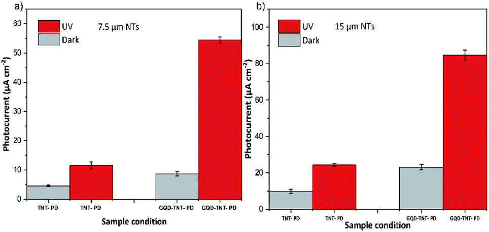 | ||
| Fig. 4 Photocurrent under dark and UV illumination conditions, without and with the application of the GQDs dual-functional blocking layer for the: (a) photodetectors with 7.5 μm TiO2 NTs, and (b) photodetectors with 15 μm TiO2 NTs. | ||
| 7.5 μm TiO2 NT | 15 μm TiO2 NT | |||||
|---|---|---|---|---|---|---|
| TNT-PD | GQD-TNT-PD | Increase | TNT-PD | GQD-TNT-PD | Increase | |
| Photocurrent (μA cm−2) | 11.52 | 54.5 | 473% | 24.3 | 85.1 | 350% |
| Responsivity (mA W−1) | 5.76 | 27.25 | 473% | 12.18 | 42.5 | 348% |
| Sensitivity (Ip − Id) Id−1 | 152.7 | 527.9 | 345% | 144.8 | 248 | 171% |
In order to obtain a deep insight into time response, stability and performance repeatability of the PEC UV photodetectors, photo response switching behaviour has been measured under illumination of on/off switching UV LEDs (360 nm, 5 mW cm−2, 6.17 mW cm−2 and 7.12 mW cm−2) and 0 V bias for the photodetectors made with 7.5 μm TiO2 NTs. The on/off switching time intervals are 15 seconds. As it is demonstrated in Fig. 5a, the photocurrent of the PEC UV photodetector made by 7.5 μm TiO2 NTs grows to a steady value under UV illumination. After switching off the UV LEDs, the photocurrent returns to the initial state in a very short time. The 4 repeated cycles indicate the reproducible characteristics of the device. In addition, the photocurrent rises as the incident photon flux increases. It is noteworthy that the increment of photocurrent is an outcome of the improved electron–hole pair generation due to an increase in incident photon flux. A similar behaviour is seen in the photo response switching plots of the GQD-TNT-PD made with 15 μm TiO2 NTs. The plots are shown in Fig. S9.† The photocurrent of the GQD-TNT-PD device was measured under different low intensity UV light. As it is shown in Fig. 5b, there is an almost linear relation between the photocurrent and the incident UV photons power intensity. This behaviour confirms that this device is applicable for detection of low intensity UV light in the self-powered mode which is an essential behaviour in many applications. For instance, as a practical method for detecting virus and bacteria, the low intensity ultraviolet emission from the biological substances need to be detected.37,38 More information about the switching performance of the other assembled PEC UV photodetectors is available in the ESI, Fig. S9.† Generally, the response speed of the device is an important factor in photodetectors. Fig. 5c and d show enlarged rising and decaying edge of the photocurrent response. The GQD-TNT-PD with 7.5 μm TiO2 NTs in the photoanode has the best response speed among various assembled devices with rise time of 0.73 s and decay time of 0.88 s. The enlarged rising and decaying edges of the photocurrent response for the GQD-TNT-PD made with 15 μm TiO2 NTs are shown in Fig. S9.† The GQD-TNT-PD with 7.5 μm TiO2 NTs in the photoanode operated 0.4–0.5 s faster in both rising and decaying behaviour compared to the device with 15 μm TiO2 NTs in the photoanode. The longer electron transport path in lengthy TiO2 NTs results in slower electron collection and thereby slower response time.
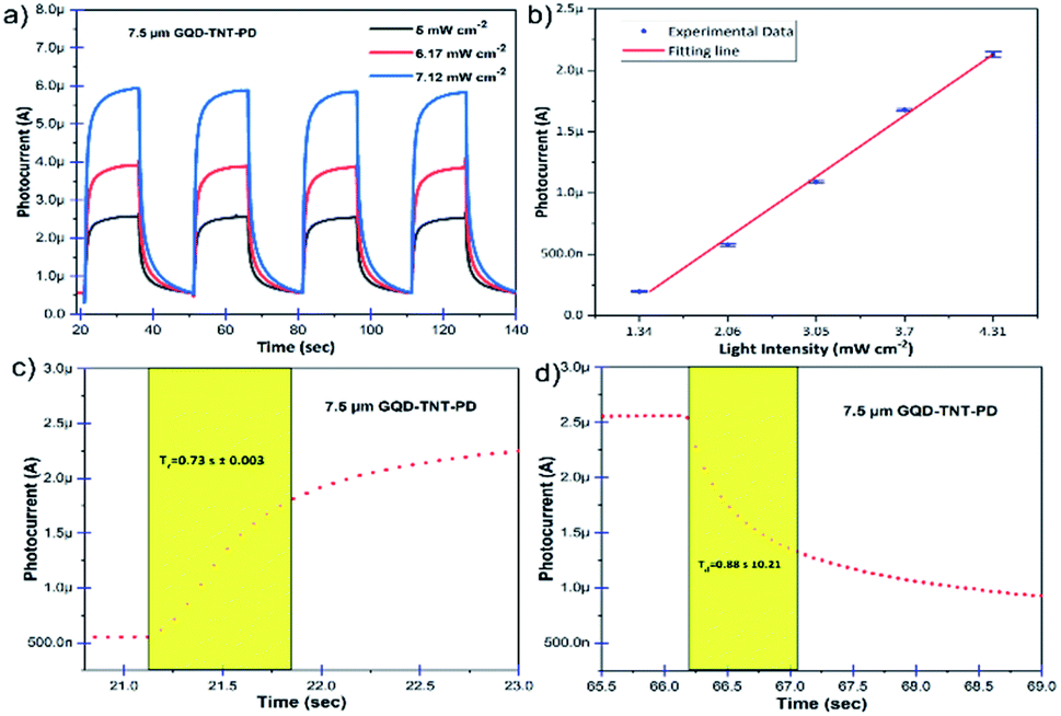 | ||
| Fig. 5 (a) Photocurrent response of the GQD-TNT-PD under on/off switching UV LEDs with the power intensity of 5, 6.17 and 7.12 mW cm−2 at 0 V bias. (b) Photocurrent of the GQD-TNT-PD as a function of light intensity, (c and d) enlarged rising and decaying edges of the GQD-TNT-PD photo response. | ||
Aiming for a deep understanding of electron transfer between interfaces, EIS was performed on the TNT-PD and the GQD-TNT-PD devices and the Nyquist plots are shown in Fig. 6a. It is quite accepted that the semicircle in the region of mid-frequencies in the Nyquist plot is affiliated with the impedance which is attributed to the charge recombination at electrolyte/photoanode interface.24 The impedance spectrum of the equivalent electrical circuit illustrated in Fig. 6b has been fitted to the Nyquist plots associated to the TNT-PD and the GQD-TNT-PD devices. The components in electrical circuit are standing for the charge transfer resistance and the capacitance of different interfaces existed in the device. For instance, Rrc and CPErc are related to the charge transfer resistance and the capacitance at the photoanode/electrolyte interface. A bigger semicircle diameter means bigger Rrc which suppress interfacial electron recombination at the mentioned interface. The obtained values for the components of the electrical circuit are reported in Table S4.† Application of the dual functional GQDs blocking layer brings about a significant increase of 289% in Rrc in the photodetector made by 7.5 μm TiO2 NTs. It is concluded that the dual functional GQDs blocking layer suppresses the charge recombination at the photoanode/electrolyte interface efficiently. The EIS Nyquist plots for the PEC UV photodetectors made with 15 μm TiO2 NTs are available in Fig. S10.† Comparing the amount of Rrc for the TNT-PD devices made with 7.5 and 15 μm TiO2 NTs, one can see that the amount of Rrc is lower for the TNT-PD device made with 15 μm TiO2 NTs, which implies the higher charge recombination in this device compared to its counterpart made by 7.5 μm TiO2 NTs. This behaviour explains the higher dark current and lower sensitivity of devices made by the 15 μm TiO2 NTs compared to the devices made by 7.5 μm TiO2 NTs. Therefore, the strategy of utilizing the GQDs coating as a dual functional layer, which can both increase the light harvesting efficiency and decrease the recombination in the device, would be considered as an efficient, practical and low-cost strategy for improving the performance of the self-powered PEC UV photodetectors.
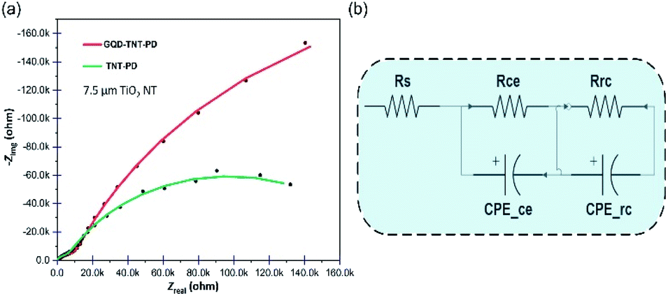 | ||
| Fig. 6 (a) EIS Nyquist plot for the 7.5 μm GQD-TNT-PD before and after sensitization with GQDs (b) equivalent circuit used for fitting the Nyquist plots in (a). | ||
Conclusions
We presented the application of a GQDs inside a PEC UV photodetector based on TiO2 NTs as a dual functional layer. The GQDs prepared by hydrothermal method and adsorbed on the surface of the TiO2 NTs through the carbonyl, carboxyl and hydroxyl (Fig. 1c) groups present on their surfaces as it is shown in Fig. 2c. The GQDs improved the responsivity and sensitivity of the self-powered PEC UV photodetector by improving the UV light absorption and suppressing the charge carrier's recombination in the photodetector. An increment of 473% in photoresponsivity has been achieved by application of GQDs in the PEC UV photodetector. It is noteworthy that the device is able to detect low intensity UV radiation (2 mW cm−2) meanwhile operating without any bias (0 V). A high value of photoresponsivity about 42.5 mA W−1 has been achieved for the PEC UV photodetector, by using 15 μm TiO2 NTs in photoanode and application of the GQDs dual-functional layer, which is significantly improved in comparison with other similar reported works reviewed in ESI, Table S5.†Author contributions
A. Z. contributed to methodology, validation, investigation, writing original draft, visualization. S. B. contributed to methodology and investigation. M. M. contributed to writing, review and editing, supervision, funding acquisition. Z. H. contributed to conceptualization, methodology, validation, writing, review and editing, visualization, supervision, project administration, funding acquisition.Conflicts of interest
There are no conflicts to declare.Notes and references
- C. H. Kang, I. Dursun, G. Liu, L. Sinatra, X. Sun and M. Kong, et al., High-speed colour-converting photodetector with all-inorganic CsPbBr3 perovskite nanocrystals for ultraviolet light communication, Light: Sci. Appl., 2019, 8(1) DOI:10.1038/s41377-019-0204-4.
- M. Qiu, P. Sun, Y. Liu, Q. Huang, C. Zhao and Z. Li, et al., Visualized UV Photodetectors Based on Prussian Blue/TiO2 for Smart Irradiation Monitoring Application, Adv. Mater. Technol., 2018, 3(2), 1–8 CrossRef.
- F. Guillemot, F. Prima, V. N. Tokarev, C. Belin, M. C. Porté-Durrieu and T. Gloriant, et al., Ultraviolet laser surface treatment for biomedical applications of β titanium alloys: Morphological and structural characterization, Appl. Phys. A: Mater. Sci. Process., 2003, 77(7), 899–904 CrossRef CAS.
- W. Lin, H. Han and H. Frei, CO2 splitting by H2O to CO and O2 under UV light in TiMCM-41 silicate sieve, J. Phys. Chem. B, 2004, 108(47), 18269–18273 CrossRef CAS.
- X. Xu, J. Chen, S. Cai, Z. Long, Y. Zhang and L. Su, et al., A Real-Time Wearable UV-Radiation Monitor based on a High-Performance p-CuZnS/n-TiO2 Photodetector, Adv. Mater., 2018, 30(43), 1–8 Search PubMed.
- Y. Gao, J. Xu, S. Shi, H. Dong, Y. Cheng and C. Wei, et al., TiO2 Nanorod Arrays Based Self-Powered UV Photodetector: Heterojunction with NiO Nanoflakes and Enhanced UV Photoresponse, ACS Appl. Mater. Interfaces, 2018, 10(13), 11269–11279 CrossRef CAS PubMed.
- Y. Ning, Z. Zhang, F. Teng and X. Fang, Novel Transparent and Self-Powered UV Photodetector Based on Crossed ZnO Nanofiber Array Homojunction, Small, 2018, 14(13), 1–9 CrossRef PubMed.
- H. Matsumoto, Photoelectrochemical Cells, Electrochem. Aspects Ionic Liq. (2nd Ed.), 2011, 414(November), 221–234 Search PubMed.
- N. L. Tarwal, V. V. Shinde, A. S. Kamble, P. R. Jadhav, D. S. Patil and V. B. Patil, et al., Photoluminescence and photoelectrochemical properties of nanocrystalline ZnO thin films synthesized by spray pyrolysis technique, Appl. Surf. Sci., 2011, 257(24), 10789–10794, DOI:10.1016/j.apsusc.2011.07.099.
- X. Li, C. Gao, H. Duan, B. Lu, Y. Wang and L. Chen, et al., High-performance photoelectrochemical-type self-powered UV photodetector using epitaxial TiO2/SnO2 branched heterojunction nanostructure, Small, 2013, 9(11), 2005–2011 CrossRef CAS PubMed.
- S. Zarei, Z. Hosseini, S. A. Sabetghadam and T. Ghanbari, Improved sensitivity in self-powered photoelectrochemical UV photodetector by application of graphene quantum dots, Eur. Phys. J. Plus, 2021, 136(5) DOI:10.1140/epjp/s13360-021-01529-2.
- X. Kong, C. Liu, W. Dong, X. Zhang, C. Tao and L. Shen, et al., Metal-semiconductor-metal TiO2 ultraviolet detectors with Ni electrodes, Appl. Phys. Lett., 2009, 94(12), 2007–2010 CrossRef.
- H. Xue, X. Kong, Z. Liu, C. Liu, J. Zhou and W. Chen, et al., TiO2 based metal-semiconductor-metal ultraviolet photodetectors, Appl. Phys. Lett., 2007, 90(20), 3–6 CrossRef.
- H. H. El-Maghrabi, A. Barhoum, A. A. Nada, Y. M. Moustafa, S. M. Seliman and A. M. Youssef, et al., Synthesis of mesoporous core-shell CdS@TiO2 (0D and 1D) photocatalysts for solar-driven hydrogen fuel production, J. Photochem. Photobiol., A, 2018, 351, 261–270, DOI:10.1016/j.jphotochem.2017.10.048.
- R. P. Vitiello, J. M. Macak, A. Ghicov, H. Tsuchiya, L. F. P. Dick and P. Schmuki, N-Doping of anodic TiO2 nanotubes using heat treatment in ammonia, Electrochem. Commun., 2006, 8(4), 544–548 CrossRef CAS.
- A. Zaleska, Doped-TiO2: A Review, Recent Pat. Eng., 2008, 2, 157–164 CrossRef CAS . Available from: www.researchgate.net/publication/TiO2/60b7d51e103e0c69cb.pdf.
- G. K. Mor, O. K. Varghese, M. Paulose, K. Shankar and C. A. Grimes, A review on highly ordered, vertically oriented TiO2 nanotube arrays: Fabrication, material properties, and solar energy applications, Sol. Energy Mater. Sol. Cells, 2006, 90(14), 2011–2075 CrossRef CAS.
- J. Xing, H. Wei, E. J. Guo and F. Yang, Highly sensitive fast-response UV photodetectors based on epitaxial TiO2 films, J. Phys. D: Appl. Phys., 2011, 44(37), 375104 CrossRef.
- T. Ji, Q. Liu, R. Zou, Y. Sun, K. Xu and L. Sang, et al., An Interface Engineered Multicolor Photodetector Based on n-Si(111)/TiO2 Nanorod Array Heterojunction, Adv. Funct. Mater., 2016, 26(9), 1400–1410 CrossRef CAS.
- P. Tiwana, P. Docampo, M. B. Johnston, H. J. Snaith and L. M. Herz, Electron mobility and injection dynamics in mesoporous ZnO, SnO2, and TiO2 films used in dye-sensitized solar cells, ACS Nano, 2011, 5(6), 5158–5166 CrossRef CAS PubMed.
- P. Roy, S. Berger and P. Schmuki, TiO2 nanotubes: Synthesis and applications, Angew. Chem., Int. Ed., 2011, 50(13), 2904–2939 CrossRef CAS PubMed.
- J. M. Macak, H. Tsuchiya, L. Taveira, S. Aldabergerova and P. Schmuki, Smooth anodic TiO2 nanotubes, Angew. Chem., Int. Ed., 2005, 44(45), 7463–7465 CrossRef CAS PubMed.
- J. Zou, Q. Zhang, K. Huang and N. Marzari, Ultraviolet photodetectors based on anodic TiO2 nanotube arrays, J. Phys. Chem. C, 2010, 114(24), 10725–10729 CrossRef CAS.
- X. Li, S. Gao, G. Wang, Z. Xu, S. Jiao and D. Wang, et al., A self-powered ultraviolet photodetector based on TiO2/Ag/ZnS nanotubes with high stability and fast response, J. Mater. Chem. C, 2020, 8(4), 1353–1358, 10.1039/c9tc05326c.
- J. Chen, B. Hu, C. Chen, X. Lv, H. San and W. Hofmann, A High-Performance Self-Powered Uv Photodetector Based On Self-Doping Tio 2 Nanotube Arrays, Pen-Tung Sah Institute of Micro-Nano Science and Technology, Xiamen University, China, Institute of Solid State Physics, Technical University of Berlin, Ber. 2019 20th Int Conf Solid-State Sensors, Actuators Microsystems Eurosensors XXXIII (TRANSDUCERS EUROSENSORS XXXIII), 2019;pp. 1329–1332 Search PubMed.
- R. Li, L. Zheng, X. Ren, J. Li and X. Qi, TiO2-graphene composite as an application of photoelectrochemical photodetectors with enhanced performances, Inorg. Nano-Met. Chem., 2021, 1–7, DOI:10.1080/24701556.2021.1897141.
- S. P. Albu, P. Roy, S. Virtanen and P. Schmuki, Self-organized TiO2 nanotube arrays: Critical effects on morphology and growth, Isr. J. Chem., 2010, 50(4), 453–467 CrossRef CAS.
- Q. Zhang, J. Jie, S. Diao, Z. Shao, Q. Zhang and L. Wang, et al., Solution-processed graphene quantum dot deep-UV photodetectors, ACS Nano, 2015, 9(2), 1561–1570 CrossRef CAS PubMed.
- L. Tang, R. Ji, X. Li, G. Bai, C. P. Liu and J. Hao, et al., Deep ultraviolet to near-infrared emission and photoresponse in layered n-doped graphene quantum dots, ACS Nano, 2014, 8(6), 6312–6320 CrossRef CAS PubMed.
- H. H. El-Maghrabi, A. A. Nada, K. R. Diab, A. M. Youssef, A. Hamdy and S. Roualdes, et al., Facile fabrication of NiTiO3/graphene nanocomposites for photocatalytic hydrogen generation, J. Photochem. Photobiol., A, 2018, 365(July), 86–93, DOI:10.1016/j.jphotochem.2018.07.040.
- S. A. Sabetghadam, Z. Hosseini, S. Zarei and T. Ghanbari, Improvement of the current generation in silicon solar cells by utilizing graphene quantum dot as spectral converter, Mater. Lett., 2020, 279, 128515, DOI:10.1016/j.matlet.2020.128515.
- X. Chu, S. Wang and Y. Cao, A new fluorescence probe comprising nitrogen-doped graphene quantum dots for the selective and quantitative determination of cerium(iv), New J. Chem., 2020, 44(3), 797–806 RSC.
- N. Hashemzadeh, M. Hasanzadeh, N. Shadjou, J. Eivazi-Ziaei, M. Khoubnasabjafari and A. Jouyban, Graphene quantum dot modified glassy carbon electrode for the determination of doxorubicin hydrochloride in human plasma, J. Pharm. Anal., 2016, 6(4), 235–241, DOI:10.1016/j.jpha.2016.03.003.
- P. Ramachandran, C. Y. Lee, R. A. Doong, C. E. Oon, N. T. Kim Thanh and H. L. Lee, A titanium dioxide/nitrogen-doped graphene quantum dot nanocomposite to mitigate cytotoxicity: synthesis, characterisation, and cell viability evaluation, RSC Adv., 2020, 10(37), 21795–21805 RSC.
- J. Xing, Y. H. Li, H. B. Jiang, Y. Wang and H. G. Yang, The size and valence state effect of Pt on photocatalytic H2 evolution over platinized TiO2 photocatalyst, Int. J. Hydrogen Energy, 2014, 39(3), 1237–1242, DOI:10.1016/j.ijhydene.2013.11.041.
- S. Min, J. Hou, Y. Lei, X. Ma and G. Lu, Facile one-step hydrothermal synthesis toward strongly coupled TiO2/graphene quantum dots photocatalysts for efficient hydrogen evolution, Appl. Surf. Sci., 2017, 396, 1375–1382, DOI:10.1016/j.apsusc.2016.11.169.
- X. Li, S. Huang and Z. Sun, Technology and equipment development in laser-induced fluorescence-based remote and field detection of biological aerosols, J. Biosaf. Biosecurity, 2019, 1(2), 113–122, DOI:10.1016/j.jobb.2019.08.005.
- K. Shirato, T. Yano, S. Senba, S. Akachi, T. Kobayashi and T. Nishinaka, et al., Detection of Middle East respiratory syndrome coronavirus using reverse transcription loop-mediated isothermal amplification (RT-LAMP), Virol. J., 2014, 11(1), 1–11 CrossRef PubMed.
Footnote |
| † Electronic supplementary information (ESI) available. See DOI: 10.1039/d2ra00379a |
| This journal is © The Royal Society of Chemistry 2022 |