DOI:
10.1039/D2RA00279E
(Paper)
RSC Adv., 2022,
12, 6848-6854
Preparation of ordered nanohole array structures by anodization of prepatterned Cu, Zn, and Ni†
Received
14th January 2022
, Accepted 24th February 2022
First published on 1st March 2022
Abstract
Anodic porous oxides with ordered nanohole array structures were prepared by the formation of concave arrays on the surface of Cu, Zn, and Ni substrates and the subsequent anodization of the prepatterned substrates. The concave arrays on the surface of the substrate were formed by Ar ion milling using an alumina mask. Although the anodization of Cu, Zn, and Ni substrates without prepatterning generates spongelike porous structures, ordered arrays of cylindrical nanoholes were obtained by the anodization of prepatterned substrates. The interpore distance of the obtained nanohole arrays was controlled by changing the period of the concave arrays. Crystallized ordered nanohole arrays of Cu2O, ZnO, and NiO were also obtained by heat treatment. The obtained anodic porous oxide with ordered nanohole array structures can be used for various applications such as photocatalysts, solar cells, and sensors.
Introduction
The formation of porous metal oxides by the anodization of metals is of increasing interest because of the wide applicability of their micro- and nanostructures for various functional devices.1–5 The functional applications of anodic porous oxides are based on the characteristic porous structures composed of a close-packed array of columnar oxide, each having a central hole.6 The formation of such structures involves the growth of the oxide layer and subsequent selective dissolution of the oxide layer. These structures were first observed in the anodization of Al, followed by other metals such as Ti, V, W, and Sn.7–14 The characteristic point of these structures from the viewpoint of their practical application is the outstanding controllability of their geometry via the anodization conditions. Typically, the hole size and interpore distance have a linear relationship with the applied voltage, and the hole depth increases with the anodization period. In addition, in some metals including Al and Ti, self-ordered structures, which have a highly ordered hole arrangement, can be obtained under appropriate anodization conditions.15–17 In contrast, in some metals, such as Cu, Zn, and Ni, the obtained anodic oxide layers show spongelike porous structures.18–20 In these metal oxides, ordered hole array structures cannot be obtained, and the control of their geometry via the anodization conditions is difficult. In the present work, we demonstrate the formation of ordered hole array structures by adopting a pretexturing process for Cu, Zn, and Ni. The pretexturing process has been used to control the sites of hole development during the anodization of metals such as Al and Ti, in which the columnar structures are spontaneously formed by anodization. In this process, the array of shallow concaves prepared by pretexturing acts as the initial site of hole development thereby generating the hole array structure with a controlled arrangement of ideally ordered or specially modified hole array structures.21–25 By investigating the anodization properties of Cu, Zn, and Ni with pretexturing patterning, we found that ordered hole array structures were successfully obtained from the pretextured pattern during the anodization. This finding enabled the formation of ordered hole array structures of anodic oxides of Cu, Zn, and Ni for the first time. The obtained samples can be used for various applications that require an ordered nanohole array composed of columnar structures such as catalysts and optical and electronic devices.
Methods
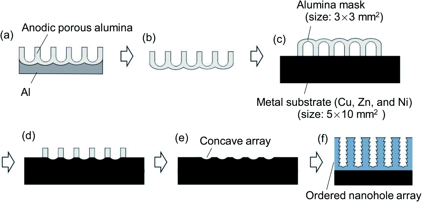
Fig. 1 shows a schematic of the preparation process for the ordered nanohole array by prepatterning metal substrates and subsequent anodization. For the formation of a shallow concave array on the surface of a metal substrate, dry etching using an anodic porous alumina mask with an interpore distance of 45, 63, or 100 nm was adopted. Anodic porous alumina masks were prepared by a two-step anodization process reported previously.26 To obtain the alumina mask with an interpore distance of 100 nm, Al was anodized in 0.3 M oxalic acid at 17 °C under a constant voltage of 40 V for 17 h. After the anodization, the oxide layer formed by the first anodization was dissolved selectively in an etchant containing 1.8 wt% phosphoric acid and 6% chromic acid at 70 °C for 2 h to obtain an Al substrate with an ordered dimple array on its surface. The arrangement of the dimple array corresponded to the hole arrangement of the anodic porous alumina obtained in the first anodization. The subsequent anodization under the same conditions as those in the first anodization generated ordered anodic porous alumina with an interpore distance of 100 nm because the dimples acted as initial points of hole development. The second anodization was performed for 2 min, after which the sample was dipped in saturated iodine methanol at 50 °C for 30 min to dissolve residual Al. The obtained alumina thin membrane was set on a metal substrate with the back surface, which is the barrier layer, facing up. Alumina masks with an interpore distance of 45 nm were formed in 8 M sulfuric acid at 18 V.27 Alumina masks with an interpore distance of 63 nm were prepared in 0.3 M sulfuric acid at 25 V.28 These masks with interpore distances of 45 and 63 nm were formed from the anodized samples and placed on the metal substrate by the same process as that for the anodic porous alumina mask with an interpore distance of 100 nm. The through-holing of the alumina mask and dry etching of the metal substrate was carried out by Ar ion milling. After the dry etching of the metal substrate, the alumina mask was detached from the substrate using adhesive tape. The prepatterned metal substrates were anodized under appropriate conditions as reported previously. Cu was anodized at 20 V in an ethylene glycol electrolyte containing 0.05 M KOH and 0.03 M NH4F at 0 °C.18 Zn was anodized at 20 V in an electrolyte with a mixture of water and ethylene glycol (1![[thin space (1/6-em)]](https://www.rsc.org/images/entities/char_2009.gif) :1 volume ratio) containing 0.1 M NaOH at 0 °C.19 Ni was anodized at 6 V in a concentrated phosphoric acid electrolyte containing 0.5 M NH4F at 16 °C.20 The obtained samples were observed by scanning electron microscopy (SEM; JSM 7500F, JEOL) at an acceleration voltage of 5 kV. The crystal structure was evaluated by X-ray diffraction (XRD; Rigaku RINT2000) with Cu Kα radiation.
:1 volume ratio) containing 0.1 M NaOH at 0 °C.19 Ni was anodized at 6 V in a concentrated phosphoric acid electrolyte containing 0.5 M NH4F at 16 °C.20 The obtained samples were observed by scanning electron microscopy (SEM; JSM 7500F, JEOL) at an acceleration voltage of 5 kV. The crystal structure was evaluated by X-ray diffraction (XRD; Rigaku RINT2000) with Cu Kα radiation.
 |
| | Fig. 1 Schematic of the preparation process for an ordered nanohole array by prepatterning of a metal substrate; (a) preparation of ordered anodic porous alumina, (b) removal of Al, (c) setting of alumina mask on a metal substrate, (d) formation of a concave array by Ar ion milling, (e) removal of alumina mask, and (f) anodization of prepatterned metal substrate. | |
Results and discussion
Fig. 2 shows SEM images of anodic porous oxides formed by the anodization of (a) Cu, (b) Zn, and (c) Ni. The metals were anodized without surface prepatterning. As can be seen from the surface and cross-sectional images of the obtained samples respectively shown on the left and right of Fig. 2, spongelike porous structures were observed in all samples.
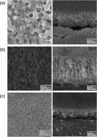 |
| | Fig. 2 SEM images of anodic porous oxides obtained by anodization of substrates without prepatterning: (a) Cu, (b) Zn, and (c) Ni. | |
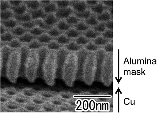
Fig. 3 shows an oblique SEM image of the Cu substrate having an alumina mask after Ar ion milling. A through-hole alumina mask was observed on the surface of the Cu substrate. Shallow concaves formed by dry etching were also observed at the bottom of the alumina holes. The interval of concaves was 100 nm, which corresponded to the interpore distance of the alumina mask. The thickness of the alumina mask was 200 nm. After the dry etching, the alumina mask was easily detached from the Cu substrate using adhesive tape.
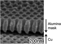 |
| | Fig. 3 Oblique SEM image of Cu substrate with alumina mask after Ar ion milling. | |
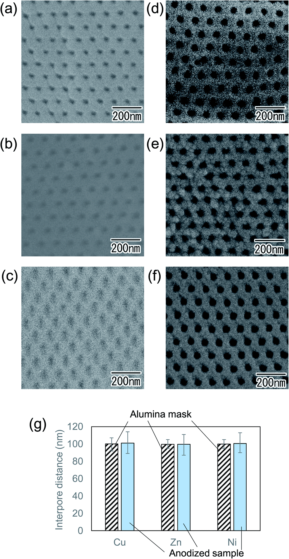
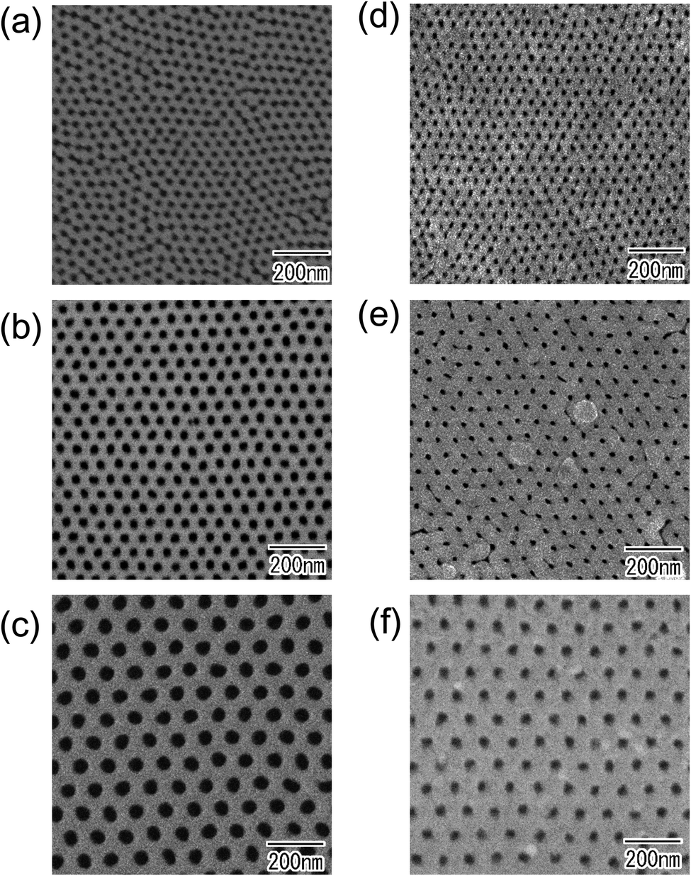
Fig. 4(a)–(c) show surface SEM images of metal substrates after Ar ion milling using an alumina mask with an interpore distance of 100 nm. Alumina mask was removed before SEM observation. As can be seen from the SEM images of (a) Cu, (b) Zn, and (c) Ni, hexagonally arranged arrays of uniform-sized concaves were observed on the surface of all metal substrates. This result indicates that the present process enables the formation of concave arrays on the surface of any metal, regardless of its hardness. Fig. 4(d)–(f) show SEM images of the surface of the samples after short anodization for 1 min. The anodization of the prepatterned substrates generated ordered nanohole arrays in all samples because each concave acted as a starting point of hole development during the initial stage of anodization. This result indicates that each surface concave promoted the formation of a cylindrical hole at the concave. Although the detailed growth mechanism of the hole array structure on the surface of these metals has not been clarified, it is thought that the concaves induced the selective dissolution of the oxide induced by a localized electric field during anodization and generated the ordered hole arrays. Fig. 4(g) shows the comparison of interpore distances between alumina masks used for Ar ion milling and anodized samples. In all samples, it was confirmed that the interpore distances of the alumina mask and the anodized samples were almost identical.
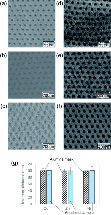 |
| | Fig. 4 SEM images of ordered concave arrays formed on (a) Cu, (b) Zn, and (c) Ni substrates after removing alumina masks. SEM images of the surface of the anodic porous oxides obtained by the anodization of (d) Cu, (e) Zn, and (f) Ni. (g) Comparison of interpore distances between alumina masks used for Ar ion milling and anodized samples. | |
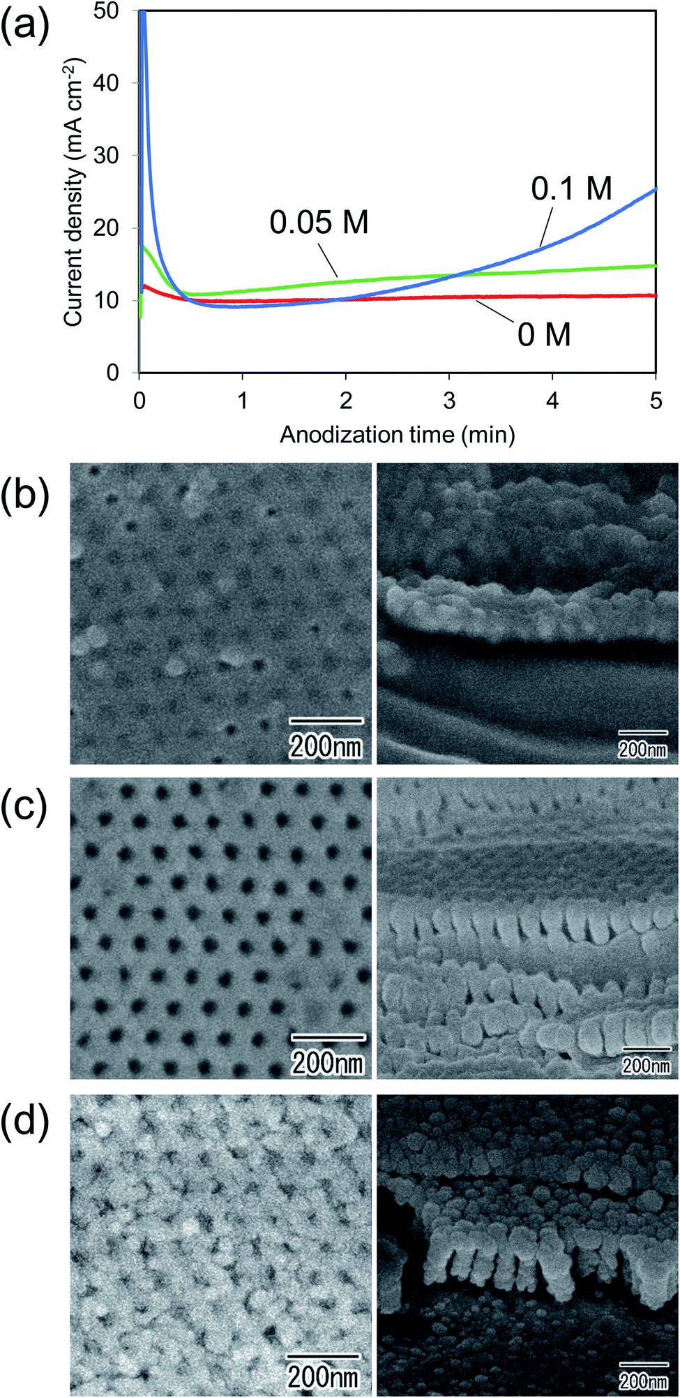
To investigate the effect of the addition of KOH in an electrolyte on the formation of ordered nanohole array structures, the composition of the electrolyte used for the anodization of Cu was changed. Fig. 5(a) shows the current density–time curves obtained during the anodization of Cu in electrolytes with different concentrations of KOH. In this experiment, the concentration of NH4F was fixed at 0.03 M, and Cu substrates were anodized for 5 min in all electrolytes. Fig. 5(a) shows that the anodization current density increased with increasing concentration of KOH. Fig. 5(b)–(d) show SEM images of the surface and cross-section of samples prepared in electrolytes with different concentrations of KOH. In the case of the sample prepared in the electrolyte without KOH shown in Fig. 5(b), an oxide film without a porous structure was formed on the surface of Cu. Generally, to form an anodic porous oxide by the anodization of a metal, the dissolution of the metal oxide by an electrolyte during anodization is required. Therefore, it is considered that no anodic porous oxide was formed by the anodization in the electrolyte without KOH because the dissolution of the Cu oxide did not proceed in the electrolyte. On the other hand, the anodization of Cu in the electrolytes containing KOH generated cylindrical holes at the shallow concaves, as shown in Fig. 5(c) and (d), and ordered hole array structures were formed in both cases. However, in the sample formed in the electrolyte containing 0.1 M KOH shown in Fig. 5(d), it was observed that the hole array structure on the surface was slightly unclear. It is thought that the concave array formed on the surface of the Cu substrate was slightly dissolved before the hole formation progressed during anodization. From these results, we concluded that the optimum concentration of KOH to obtain a uniform oxide film with an ordered nanohole array structure is 0.05 M. Results of similar investigations on the effect of the concentration of NH4F in the electrolyte indicated that 0.03 M was the optimum concentration for the preparation of ordered nanohole array structures of Cu oxide (Fig. S1†).
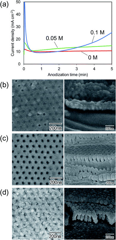 |
| | Fig. 5 (a) Current density–time curves. Surface and cross-sectional SEM images of anodic oxide obtained by anodization of Cu in electrolytes containing (b) 0, (c) 0.05, and (d) 0.1 M KOH. | |
Fig. 6 shows SEM images of samples obtained by the anodization of Cu for (a) 1, (b) 5, and (c) 10 min in an electrolyte containing 0.05 M KOH and 0.03 M NH4F at 20 V. The SEM images shown in Fig. 6(a) and (b) indicate that an ordered nanohole array structure was obtained within 5 min. In the first 5 min of anodization, the hole depth of the ordered nanohole array increased with increasing anodization time. However, the surface of the sample obtained by 10 min anodization was rough, and the ordered nanohole array structure disappeared owing to the dissolution of the surface of the sample. The spongelike porous structure was also observed at the bottom of the sample.
 |
| | Fig. 6 SEM images of anodized porous Cu oxide prepared by anodization of Cu for (a) 1, (b) 5, and (c) 10 min. | |
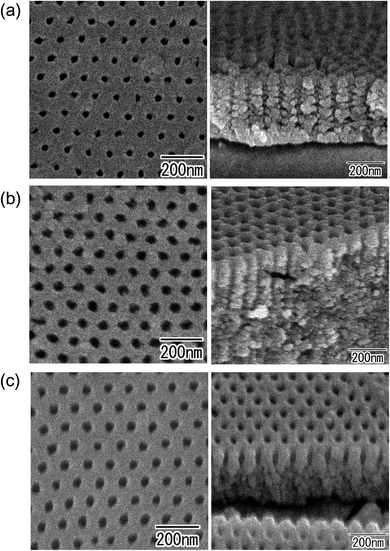
Fig. 7 shows surface SEM images of the alumina masks with different interpore distances used for the dry etching and the anodic porous Cu oxides obtained by the subsequent anodization. For the patterning of the Cu substrates, alumina masks with interpore distances of (a) 45, (b) 63, and (c) 100 nm were used. From the SEM images of the samples after anodization shown in Fig. 7(d)–(f), it was confirmed that the interpore distances of the nanohole array structures obtained by anodization were also (d) 45, (e) 63, and (f) 100 nm. These values were in good agreement with the interpore distances of the alumina mask used for the dry etching. In this experiment, the Cu substrates with arrays of concaves with different periods were anodized at the same voltage of 20 V. The interpore distance of the anodic porous Cu oxide was controlled by adjusting the period of the array of concaves formed on the surface of the Cu substrate. These results indicate that in the anodization of a Cu substrate with a patterned surface, the hole development was determined by the pretexturing pattern regardless of the applied voltage. Similar results were observed for the anodization of Zn and Ni. The interpore distance of the anodic porous oxides obtained by the anodization of Zn and Ni were also controlled by changing the period of the array of concaves formed on the substrate.
 |
| | Fig. 7 SEM images of alumina masks with interpore distances of (a) 45, (b) 63, and (c) 100 nm. SEM images of anodic porous Cu oxide with interpore distances of (d) 45, (e) 63, and (f) 100 nm. | |
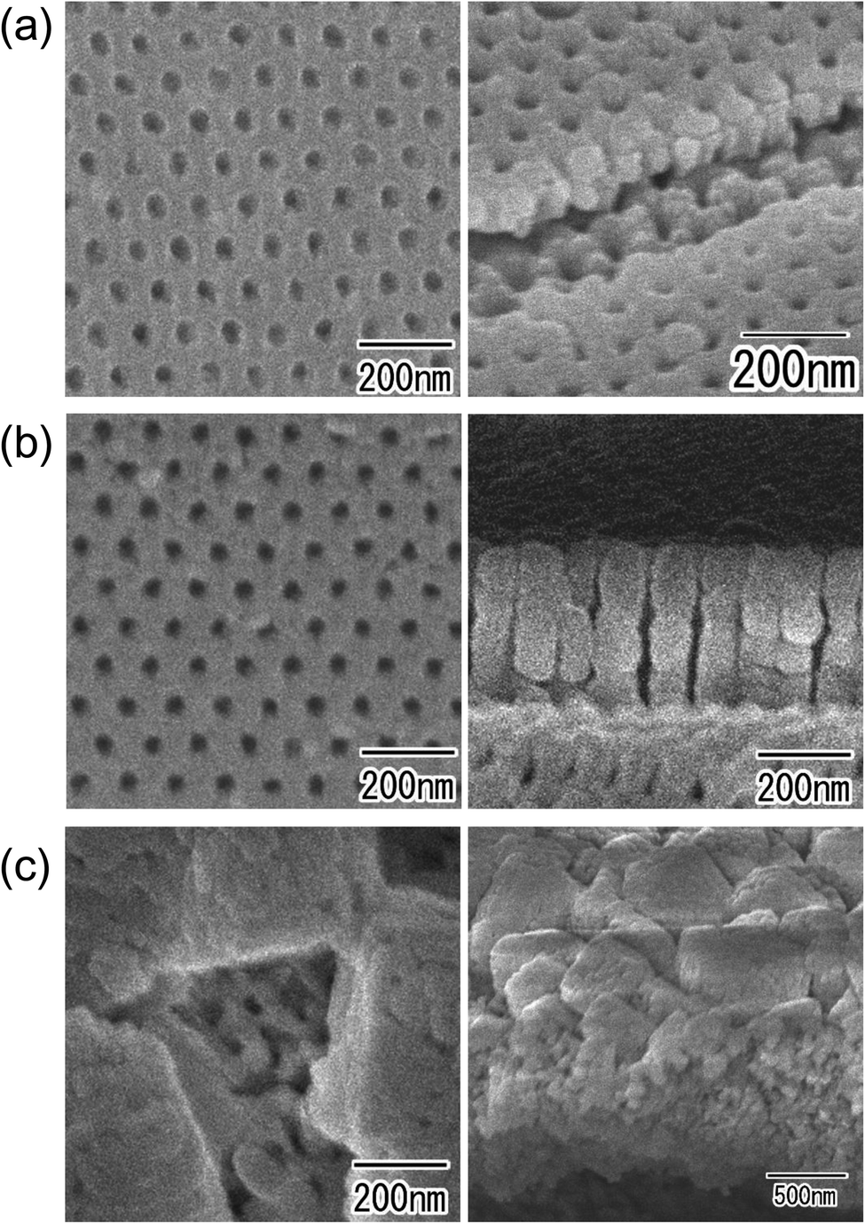
Fig. 8 shows SEM images of ordered nanohole arrays obtained by the anodization of (a) Cu, (b) Zn, and (c) Ni under optimized conditions. Prior to the anodization, an ordered array of shallow concaves was formed by Ar ion milling using an alumina mask with an interpore distance of 100 nm. The hole depths of the ordered nanohole arrays in Fig. 8(a)–(c) were 400, 350, and 150 nm, respectively. In all samples, spongelike porous structures were observed under the ordered nanohole arrays. Further optimization of the anodization conditions is expected to enable the formation of nanohole arrays with higher aspect ratios.
 |
| | Fig. 8 (a) SEM images of ordered anodic porous Cu oxide prepared by anodization of Cu at 20 °C in an electrolyte with a mixture of ethylene glycol and glycerol (1:1 volume ratio) containing 0.05 M KOH and 0.03 M NH4F at 0 °C for 15 min. (b) SEM images of ordered anodic porous Zn oxide prepared by anodization of Zn at 20 V in an electrolyte with a mixture of ethylene glycol and water (1:1 volume ratio) containing 0.1 M NaOH at 0 °C for 30 min. (c) SEM images ordered anodic porous Ni oxide of prepared by anodization of Ni at 6 V in concentrated phosphoric acid containing 0.5 M NH4F at 16 °C for 10 min. | |
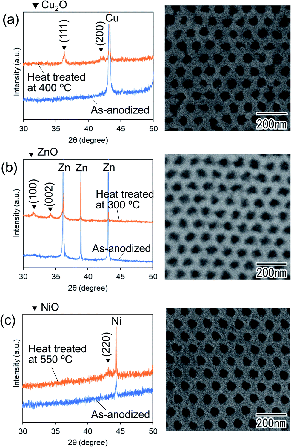
Although oxide films obtained by anodization are generally amorphous, crystallized oxide films can be obtained by heat treatment after anodization. Fig. 9 shows XRD patterns and SEM images of ordered nanohole arrays obtained by the anodization of Cu, Zn, and Ni after heat treatment in a N2 atmosphere. Heat treatment of the samples was performed at 400, 300, and 550 °C for Cu, Zn, and Ni, respectively. From the XRD patterns, it was confirmed that the crystal phase of the samples changed from the amorphous phase to (a) Cu2O, (b) ZnO, and (c) NiO after heat treatment. The ordered hole array structures of all samples were maintained even after heat treatment. The obtained crystallized nanohole arrays composed of Cu2O, ZnO, and NiO can be applied to various functional devices because of their semiconducting properties.
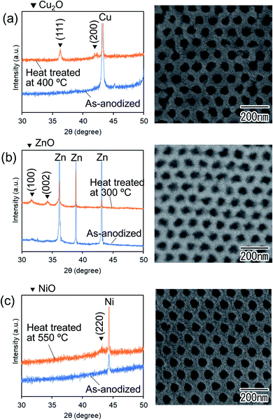 |
| | Fig. 9 XRD patterns and SEM images of heat-treated nanohole arrays of (a) Cu2O, (b) ZnO, and (c) NiO. | |
Conclusions
Ordered anodic porous oxides of Cu, Zn, and Ni were obtained by performing a pretexturing process before anodization. The interpore distance of the nanohole array structures was controlled by changing the period of the concave arrays formed on their surface. The ordered nanohole array structures obtained by this process were also maintained even after crystallization by heat treatment. The obtained anodic porous oxides with ordered nanohole array structures can be used for various applications, such as photocatalysts, solar cells, and batteries.
Conflicts of interest
There are no conflicts to declare.
Acknowledgements
The present work was supported by the Murata Science Foundation.
References
- C. A. Huber, T. E. Huber, M. Sadoqi, J. A. Lubin, S. Manalis and C. B. Prater, Nanowire Array Composites, Science, 1994, 263, 800 CrossRef CAS PubMed.
- S. H. Jeong, H. Y. Hwang, K. H. Lee and Y. Jeong, Template-Based Carbon Nanotubes and Their Application to a Field Emitter, Appl. Phys. Lett., 2001, 78, 2052 CrossRef CAS.
- A. Kolmakov, Y. Zhang, G. Cheng and M. Moskovits, Detection of CO and O2 Using Tin Oxide Nanowire Sensors, Adv. Mater., 2003, 15, 997 CrossRef CAS.
- E. M. I. M. Ekanayake, D. M. G. Preethichandra and K. Kaneto, Polypyrrole Nanotube Array Sensor for Enhanced Adsorption of Glucose Oxidase in Glucose Biosensors, Biosens. Bioelectron., 2007, 23, 107 CrossRef CAS PubMed.
- Y. Cao and T. E. Mallouk, Morphology of Template-Grown Polyaniline Nanowires and Its Effect on the Electrochemical Capacitance of Nanowire Arrays, Chem. Mater., 2008, 20, 5260 CrossRef CAS.
- F. Keller, M. S. Hunter and D. L. Robinson, Structural Features of Oxide Coatings on Aluminum, J. Electrochem. Soc., 1953, 100, 411 CrossRef CAS.
- P. Roy, S. Berger and P. Schmuki, TiO2 Nanotubes: Synthesis and Applications, Angew. Chem., Int. Ed., 2011, 50, 2904 CrossRef CAS PubMed.
- H. Tsuchiya, J. M. Macak, I. Sieber and P. Schmuki, Self-Organized High-Aspect-RatioNanoporous Zirconium Oxides Prepared by Electrochemical Anodization, Small, 2005, 1, 722 CrossRef CAS PubMed.
- M. Altomare, O. Pfoch, A. Tighineanu, R. Kirchgeorg, K. Lee, E. Selli and P. Schmuki, Molten o-H3PO4: A New Electrolyte for the Anodic Synthesis of Self-Organized Oxide Structures – WO3 Nanochannel Layers and Others, J. Am. Chem. Soc., 2015, 137, 5646 CrossRef CAS PubMed.
- W. Wei, J. M. Macak, N. K. Shrestha and P. Schmuki, Thick Self-Ordered Nanoporous Ta2O5 Films with Long-Range Lateral Order, J. Electrochem. Soc., 2009, 156, K104 CrossRef CAS.
- A. Palacios-Padrós, M. Altomare, A. Tighineanu, R. Kirchgeorg, N. K. Shrestha, I. Díez-Pérez, F. Caballero-Briones, F. Sanz and P. Schmuki, Growth of ordered anodic SnO2 nanochannel layers and their use for H2 gas sensing, J. Mater. Chem. A, 2014, 2, 915 RSC.
- R. Kirchgeorg, S. Berger and P. Schmuki, Ultra Fast Electrochromic Switching of Nanoporous Tungsten–Tantalum Oxide Films, Chem. Commun., 2011, 47, 1000 RSC.
- Z. Li, D. Ding, Q. Liu, C. Ning and X. Wang, Ni-Doped TiO2 Nanotubes for Wide-Range Hydrogen Sensing, Nanoscale Res. Lett., 2014, 9, 118 CrossRef PubMed.
- N. T. Nguyen, I. Hwang, T. Kondo, T. Yanagishita, H. Masuda and P. Schmuki, Optimizing TiO2 Nanotube Morphology for Enhanced Photocatalytic H2 Evolution Using Single-Walled and Highly Ordered TiO2 Nanotubes Decorated with Dewetted Au Nanoparticles, Electrochem. Commun., 2017, 79, 46 CrossRef CAS.
- H. Masuda and K. Fukuda, Ordered Metal Nanohole Arrays Made by a Two-Step Replication of Honeycomb Structures of Anodic Alumina, Science, 1995, 268, 1466 CrossRef CAS PubMed.
- J. M. Macak, S. P. Albu and P. Schmuki, Towards Ideal Hexagonal Self-Ordering of TiO2 Nanotubes, Phys. Status Solidi, 2007, 1, 181 CAS.
- M. Iwai, T. Kikuchi and R. O. Suzuki, Self-Ordered Nanospike Porous Alumina Fabricated Under a New Regime by an Anodizing Process in Alkaline Media, Sci. Rep., 2021, 11, 7240 CrossRef CAS PubMed.
- D. P. Oyarzún Jerez, M. L. Teijelo, W. R. Cervantes, O. E. L. Pérez, J. Sánchez, G. C. Pizarro, G. Acosta, M. Flores and R. Arratia-Perez, Nanostructuring of Anodic Copper Oxides in Fluoride-Containing Ethylene Glycol Media, J. Electroanal. Chem., 2017, 807, 181 CrossRef.
- S. Ono, Y. Kobayashi and H. Asoh, Self-Organized and High Aspect Ratio Nanoporous Zinc Oxide Prepared by Anodization, ECS Trans., 2008, 13, 183 CrossRef CAS.
- N. K. Shrestha, M. Yang and P. Schmuki, Self-Ordered Nanoporous Nickel Oxide/Fluoride Composite Film with Strong Electrochromic Contrast, Electrochem. Solid-State Lett., 2010, 13, C21 CrossRef CAS.
- H. Masuda, H. Yamada, M. Satoh, H. Asoh, M. Nakao and T. Tamamura, Highly Ordered Nanochannel-Array Architecture in Anodic Alumina, Appl. Phys. Lett., 1997, 71, 2770 CrossRef CAS.
- T. Yanagishita, A. Kato and H. Masuda, Preparation of Ideally Ordered Through-Hole Anodic Porous Alumina Membranes by Two-Layer Anodization, Jpn. J. Appl. Phys., 2017, 56, 035202 CrossRef.
- T. Kondo, S. Nagao, S. Hirano, T. Yanagishita, N. T. Nguyen, P. Schmuki and H. Masuda, Fabrication of Ideally Ordered Anodic Porous TiO2 by Anodization of Pretextured Two-Layered Metals, Electrochem. Commun., 2016, 72, 100 CrossRef CAS.
- T. Yanagishita, H. Hirose, T. Kondo, P. Schmuki and H. Masuda, Fabrication of Ideally Ordered TiO2 Through-Hole Membranes by Two-Layer Anodization, RSC Adv., 2020, 10, 37657 RSC.
- T. Yanagishita, T. Masuda, T. Kondo and H. Masuda, Highly Ordered Anodic Porous Oxide of Transition Metals Fabricated by Anodization Combined with Pretexturing Process, Electrochem. Commun., 2021, 123, 106916 CrossRef CAS.
- H. Masuda and M. Sato, Fabrication of Gold Nanodot Array Using Anodic Porous Alumina as an Evaporation Mask, Jpn. J. Appl. Phys., 1996, 35, 126 CrossRef.
- H. Masuda, M. Nagae, T. Morikawa and K. Nishio, Long-Range-Ordered Anodic Porous Alumina with Reduced Hole Interval Formed in Highly Concentrated Sulfuric Acid Solution, Jpn. J. Appl. Phys., 2006, 45, L406 CrossRef CAS.
- H. Masuda, H. Hasegawa and S. Ono, Self-Ordering of Cell Arrangement of Anodic Porous Alumina Formed in Sulfuric Acid Solution, J. Electrochem. Soc., 1997, 144, L127 CrossRef CAS.
Footnote |
| † Electronic supplementary information (ESI) available. See DOI: 10.1039/d2ra00279e |
|
| This journal is © The Royal Society of Chemistry 2022 |
Click here to see how this site uses Cookies. View our privacy policy here. 
 Open Access Article
 This Open Access Article is licensed under a Creative Commons Attribution-Non Commercial 3.0 Unported Licence
 *,
Takuya Masuda and
Hideki Masuda
*,
Takuya Masuda and
Hideki Masuda