
 Open Access Article
 This Open Access Article is licensed under a Creative Commons Attribution-Non Commercial 3.0 Unported Licence
Vacuum-free solution-based metallization (VSM) of a-IGZO using trimethylaluminium solution†
Taehoon Sung,
Min-Kyu Song,
Se-Yeon Jung,
Sein Lee,
Young-Woong Song ,
Solah Park and
Jang-Yeon Kwon*
,
Solah Park and
Jang-Yeon Kwon*
School of Integrated Technology, Yonsei University, 50, Yonsei-ro, Seodaemun-gu, Seoul, Republic of Korea. E-mail: jangyeon@yonsei.ac.kr
First published on 27th January 2022
Abstract
This research demonstrates a method to reduce the resistance of amorphous indium–gallium–zinc–oxide (a-IGZO) using a “vacuum-free solution-based metallization” (VSM) process, which revolutionizes the metallization process thanks to its simplicity, by simply dipping the a-IGZO into trimethyl aluminium (TMA, (CH3)3Al) solution. From the XPS results, it was found that oxygen vacancies were generated after the VSM process, resulting in the enhanced conductivity. Various metallization time and solution temperature conditions were investigated, and the measured conductivity of the a-IGZO could be enhanced up to 20.32 S cm−1, which is over 105 times larger compared to that of the untreated a-IGZO. By utilizing the VSM process, self-aligned top-gate (SATG) a-IGZO thin-film-transistors (TFTs) were successfully fabricated, and to provide an explanation for the mechanism, X-ray photoelectron spectroscopy (XPS) was employed.
Introduction
With the increasing demand for the future displays, amorphous oxide semiconductors (AOSs) have received much attention in the field of displays as alternatives for silicon semiconductors due to their high on/off ratio, high electron mobility, high uniformity and low fabrication temperature.1–8 Thanks to such advantages, amorphous–indium–gallium–zinc–oxide (a-IGZO) is currently being widely used as driving and switching transistors (TRs) in display backplanes.9–13As the future displays often require a resolution of over 8 K (7680 × 4320 pixels) and refreshing rate of over 240 Hz, the switching speed required for the TRs is often less than a few μs.14 Such an ever demanding switching speed requirement cannot be easily met with the conventional TFT structure, where the gate electrode and source & drain (S&D) electrodes overlap, due to high parasitic capacitance.15 Therefore, self-aligned top-gate (SATG) thin-film transistors (TFT) have been set as an industry standard thanks to their very low parasitic capacitance, which originates from having almost zero overlap between the gate electrode and the S&D electrodes.16–19
However, the SATG TFTs using AOSs can't function without the proper metallization process, since the resistance of the pristine AOSs is too high to be used as conductors. Therefore, the conductivity of the S&D region of the SATG TFTs must be enhanced to ensure lower contact resistance and high current flow through the S&D electrodes.15,20 Otherwise, the source-to-drain electrical field may suffer from the voltage drop mostly occurring in the high-resistance S&D region, and therefore increasing the power consumption, and decreasing the current flow through the active region.18,21 The decrease in the on-current also results in the decrease in the calculated field-effect mobility.
Various research groups have proposed effective techniques to metallize the AOSs, and such techniques include implantation,22–24 UV exposure,25–27 and plasma treatment.21,28–30 Although the proposed techniques successfully metallize the AOSs, each method possesses unique challenges.21 For example, the implantation method not only requires additional equipment for implantation but also requires high temperature annealing for activation. Additionally, the UV exposure method may induce unwanted high energy light absorption in the semiconductor–gate insulator stack, which may lead to bias stress instabilities. Furthermore, the plasma treatment method often induces unwanted migration of hydrogen species into the channel region, which often results in excessively populated carrier concentration in the channel region.
Recent research proposes metal-induced metallization by using reductive metals such as aluminium (Al), titanium (Ti), and magnesium (Mg).21,31–36 Highly reductive nature of these metals can be confirmed by standard reduction potential (E°) of metal ions and Gibbs free energy of formation  of metal oxides that are shown in Table 1. Even though those reductive metals are excellent candidates to chemically reduce a-IGZO, they are mostly deposited in rather complex high vacuum environment to prevent unwanted oxidation, and high temperature activation annealing is often required to enhance the conductivity to a sufficient level. Such annealing often induces defect diffusion from the metallization region to the channel region.29,37–39
| Ions | E° (V) | Oxides |
|
|---|---|---|---|
| In3+ | −0.34 | In2O3 | −830.7 |
| Ga3+ | −0.56 | Ga2O3 | −998.4 |
| Zn2+ | −0.76 | ZnO | −320.6 |
| Al3+ | −1.66 | Al2O3 | −1582.3 |
| Ti2+ | −1.63 | TiO2 | −889.1 |
| Mg2+ | −2.37 | MgO | −569.3 |
| Li+ | −3.05 | Li2O | −562.1 |

Additionally, most previously reported literature about solution-processed oxide semiconductors mainly focuses on deposition of the oxide semiconductors,40,41 while the proposed metallization process in this paper solely focuses on the metallization of already deposited oxide semiconductors. Since the mechanism of the metallization process is mainly a redox reaction between the Al incorporated in the oxide semiconductor and metal species in the oxide semiconductor, it is believed that the proposed metallization process is widely applicable regardless of the oxide semiconductors' deposition method.
In this research, a novel, cost effective and solution processable approach, which incorporates chemical reduction of a-IGZO using trimethyl aluminium (TMA) solution, namely “vacuum-free solution-based metallization” (VSM), was investigated. Since the VSM process only requires simply dipping the a-IGZO into the TMA solution, there is no need to install and maintain costly and bulky vacuum chambers and their accessories. Although this research mainly focuses on the metallization of a-IGZO, by controlling the temperature and the time, the degree of the metallization can be changed, which grants us better controllability over the conductivity of a-IGZO. Additionally, the conductivity enhancement achieved by the VSM process is comparable to the conductivity achieved by conventional metallization methods. Therefore, the VSM process proposed in this manuscript is simple yet effective. The conductivity was first measured to confirm the enhanced conductivity of a-IGZO, then subsequent integration of the VSM process to the TFTs fabrication was followed. Lastly, peaks from XPS measurement were analysed to clarify the underlying mechanism of the TMA-solution metallization process.
Experimental
SATG fabrication
Silicon wafer with 300 nm-thick thermally grown SiO2 was used as a substrate. The substrate was cleansed in acetone, isopropyl alcohol (IPA) and distilled (D.I.) water for 10 minutes each. Then 30 nm-thick a-IGZO layer was deposited as an active layer on the substrate using radio frequency (RF) sputtering with oxygen partial pressure of 20%. After the a-IGZO deposition, the samples went through a-IGZO etching process using HCl as an etchant, followed by annealing at 300 °C for 1 h in ambient air. Plasma-enhanced chemical vapor deposition (PE-CVD) was utilized to deposit 100 nm-thick SiO2 gate insulator (G.I.) at 300 °C. Molybdenum (Mo) gate electrode was deposited using direct current (DC) sputtering and patterned using a lift-off process. After that, the G.I. was etched using the gate electrode as a mask using inductively coupled plasma reactive ion etching (ICP-RIE), therefore forming a self-aligned active region. Again, DC sputtering and a lift-off process were used to form 100 nm-thick Mo S&D electrodes. The defined channel region was 100 × 50 μm, and the gaps between the channel and the S&D electrodes were 30 μm each. Optical microscopic image and 3-D structure of the fabricated TFT sample are shown in Fig. 1a and b. | ||
| Fig. 1 (a) Optical microscopic image of the fabricated SATG TFT, and (b) 3-D schematic that shows the structure of the SATG TFT. Note that the underlapping IGZO must be metallized to fabricate a functional SATG TFT. As a proof that the SATG TFT was fabricated as intended, TEM images and EDS data of the TFT stack and the metallized IGZO are shown in (c) and (d), respectively. | ||
Additionally, tag patterns for the a-IGZO's conductivity measurement were also formed simultaneously on the same substrate during the SATG fabrication process by placing a 30 nm-thick a-IGZO layer between 100 nm-thick Mo electrodes. Width and length of the a-IGZO in the tag patterns are 100 μm and 50 μm, respectively.
VSM process
The fabricated SATG samples were put in a glove box filled with argon (Ar) (H2O < 1 ppm). Each sample was placed individually in a glass vial, and each vial was filled with 10 ml of the TMA solution (2.0 M in toluene, Sigma-Aldrich). The vials were quickly closed with polytetrafluoroethylene (PTFE) coated polypropylene (PP) screw caps to prevent TMA from reacting with oxygen and water molecules that may reside in the glove box. Then the vials were placed on hot plates where the temperature was set in advance accordingly. After undergoing the metallization process for a desired amount of time, the samples were cleansed with toluene and blown with Ar in the glove box.Results and discussion
Conductivity measurement
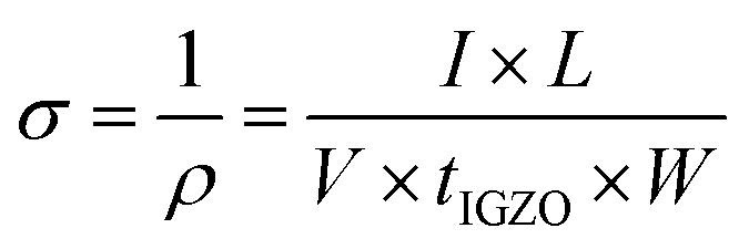
To analyse how well the TMA solution metallizes a-IGZO, 2-point conductivity was measured. The conductivity (α) was calculated using eqn (1),
 | (1) |
The calculated conductivity of the untreated sample and the VSM-processed samples is shown in Fig. 2. By simply putting the a-IGZO in the TMA solution for 15 minutes at 30 °C, enhanced conductivity was achieved. To accelerate the metallization and to further enhance the conductivity, additional heating was introduced. As the graph shows, the conductivity is enhanced faster when the temperature is higher. In all the temperature range, increased metallization time results in further enhanced conductivity. By changing the solution temperature, the speed of the metallization process can be adjusted while changing the time affects the degree of the metallization. Therefore, by controlling both the temperature and time, the conductivity of the a-IGZO can be precisely controlled.
 | ||
| Fig. 2 Time-dependent conductivity change of the samples treated in 30, 70, and 110 °C. The conductivity was enhanced by 1.97 × 10⁵ times after the VSM process in 110 °C for 180 minutes. | ||
By maximizing the temperature and time to fully metallize a-IGZO, very high conductivity of 20.32 S cm−1 was achieved from the sample that underwent through the VSM process for 180 min at 110 °C. The measured conductivity is approximately 1.97 × 10⁵ times larger than that of the untreated sample (1.03 × 10⁻⁴ S cm−1). Since the boiling point of toluene is known to be 110.6 °C, 110 °C was technically the maximum temperature able to be investigated safely. Since the conductivity was not enhanced in a sample treated with only the toluene solvent as shown in Fig. S1,† the conductivity enhancement effect is believed to be mostly derived from the TMA in the solution instead of the solvent.
Unlike other transition metal-based metallization methods, the proposed VSM process does not require additional heat treatment after the metallization. Additionally, considering that the VSM process is solution-based, requiring only 3 hours for the metallization is fast enough to be integrated in the TFT fabrication process. To confirm the compatibility with the TFT fabrication process, we have fabricated TFTs by incorporating the VSM process as a method to metallize the S&D region.
TFT characterization
Graphs from Fig. 3a show combined transfer curves of samples that were metallized in 30 °C, 70 °C and 110 °C. Each graph contains transfer curves with different metallization time, namely from 0 minutes (untreated) to 180 minutes. Parameters of the transfer curves of the samples that were metallized in 110 °C are shown in Fig. 3b. | ||
| Fig. 3 (a) Transfer curves from the VSM-metallized SATG TFTs, and (b) parameters from the TFTs that were metallized in 110 °C drawn in terms of the metallization time. | ||
As the temperature or the metallization time increases, on-current level increases. This is probably due to the increased conductivity of the VSM-processed a-IGZO S&D region, as we could confirm that the conductivity of a-IGZO increases further as the metallization time or temperature increases. Such increase in the on-current level leads to enhanced mobility, since the calculated mobility (μ) is largely affected by the drain current (ID) level according to the following equation,
 | (2) |
In terms of the threshold voltage (Vth), the Vth was 6.16 V for the sample metallized in 110 °C for 15 minutes, and 6.31 V for the sample metallized in 30 °C for 180 minutes. However, the sample metallized in 110 °C for 180 minutes showed the negatively shifted Vth value of −0.32 V. Increase in the metallization time or the temperature induces negative shift of the Vth. This is probably due to slight migration of carriers that reside in the metallized S&D region of the a-IGZO film into the channel region of the a-IGZO film. Such behaviour is easily observable in other literature as well,29,35,37 and it is due to the carrier concentration gradient formed inherently between the metallized S&D region and the channel region.
As shown in Fig. 3a and b, the off-current, which is mostly incurred due to the gate leakage, generally increases as the metallization time or temperature increases. This is probably due to the combined effects of decreased resistance of SiO2 around the edges and increased overall current level at the S&D region. Although existence of Al was found in the TEM-EDS results as shown in Fig. 1c and d, it is believed not to be metallic since the increase in the off-current is not as drastic as the increase in the on-current or the conductivity of the VSM-processed a-IGZO. If the metallic Al was precipitated on the surface of the TFTs, the entire surface of the TFTs should be conductive. Functioning TFTs cannot be achieved with the existence of uncontrollable current pathways,42 which include leakage paths from the gate electrode to the S&D electrodes and from the source electrode to the drain electrode.
Since the only reasonable current path of the gate leakage is from the gate electrode to either the drain or the source electrode, the enhanced conductivity of the metallized a-IGZO region should be at least partly responsible for the increased gate leakage.
XPS measurement
From the XPS-depth analysis shown in Fig. S2,† the apparent oxygen concentration was not found to be lower in the samples with higher metallization temperature. Instead, Al was found to be incorporated in the a-IGZO layer. Incorporation of Al has been also confirmed in time-of-flight secondary ion mass spectroscopy (ToF-SIMS) data as shown in Fig. S3.† As we have confirmed in TEM or optical microscopic images in Fig. 1, no significant amount of Al was found on the surface of the VSM-processed a-IGZO. Therefore, deposition of a conductive Al layer is highly unlikely, and the conductivity enhancement in VSM process was not achieved simply by the deposition of a metallic layer.In addition, Al incorporated in the a-IGZO layer was found to be in an oxidized state as shown in Fig. S4a.† The Al 2p peaks found in the VSM-processed samples tend to have the peak values of around 75 eV, which is closer to oxidized Al species' peak values such as Al2O3 (74.1 eV), Al(OH)3 (74.8 eV), AlO(OH) (75.2 eV), than it is to metallic Al's peak value that is known to be around 72.7 eV. In terms of atomic ratio, more Al was found in samples that were metallized in higher temperature as shown in Fig. S4b.†
To further analyse the origin of the conductivity enhancement, O 1s peaks were deconvoluted into three subpeaks. The first subpeak found at around 529 eV (O1 peak) represents lattice oxygen in a-IGZO, the second peak at around 530 eV (O2 peak) represents the oxygen vacancy, and the third subpeak at around 531 eV (O3 peak) represents loosely bound oxygen impurities.43–46 During the deconvolution process, the full-width half-maximum of each subpeak was set around 1.6 eV to ensure accurate fit results.47
As shown in Fig. 4a and b, the relative peak area of the O2 peak becomes significantly larger as the solution temperature rises. In addition, as shown in Fig. S5b,† the relative peak area of the O3 peak becomes smaller as the temperature increases. From the understanding on how each peak is related to the movement of the oxygen species in AOSs, we could predict how the VSM process affects the a-IGZO. It is known that the increase in the oxygen vacancy concentration induces increased carrier generation due to the oxygen vacancy's donor like behaviour in most AOSs.48 On the other hand, the loosely bound oxygen often acts as a charge trap, which reduces the current level.49 Therefore, the XPS results agree well with the results from the conductivity measurement, where the conductivity was increased faster and even further when the solution temperature was higher. In addition, in Fig. S5a,† slight increase in the relative area of O1 peaks is also noticeable as the temperature rises. This is probably due to slight annealing effect that is induced during the VSM process at heated conditions.13,27,43
 | ||
| Fig. 4 XPS analysis of samples. (a) Deconvoluted O 1s spectra of the samples VSM-processed under different temperatures, and (b) calculated relative peak area of O2 subpeak. Increase in the O2 subpeak area indicates formation of oxygen vacancies. (c) Deconvoluted O 1s spectra of the 110 °C, 3 h sample for the depth analysis. Graphs in (d) indicates the relative O2 subpeak area change in relation to the etch time. Surface of the a-IGZO seems to be more metallized than the bulk of the a-IGZO. | ||
O 1s peak spectra from the XPS-depth analysis of the sample that was VSM-processed at 110 °C for 3 h were further analysed. From 150 s to 750 s, O 1s peaks were deconvoluted again into the three subpeaks. Interestingly, the highest relative peak area of the O2 peak was found near at the surface of the a-IGZO, as shown in Fig. 4c and d. This proves that the TMA solution used in the VSM process takes oxygen mostly from the surface of the a-IGZO, where active exchange of materials may occur. In Fig. S5c,† the O1 peaks show slight increase in their relative area, while Fig. S5d† shows decrease in the O2 relative peak area as the etch time increases. This indicates that the bulk of the a-IGZO is more stoichiometric than the surface of the a-IGZO, where the loosely bound oxygen and oxygen vacancy are more frequently present. Such concentration gradient formed along the thickness of the a-IGZO means that the reaction between the TMA and oxygen in a-IGZO mostly occurs near the surface of a-IGZO.
From the XPS analysis, oxygen species in the a-IGZO were studied and the relationship between the electrical conductivity enhancement and materialistic change could be established. The schematics of the proposed mechanism are shown in Fig. 5 to help visualizing it. From the results that the concentration of the oxygen vacancy showed huge increase after the VSM process, where the O2/Ototal increased from the 58.91% of the untreated sample to 75.39% of the sample that is VSM-processed at 110 °C for 3 h, and that the concentration of the oxygen vacancy is higher at the surface of the a-IGZO, it can be concluded that the TMA mostly takes up oxygen (especially loosely bound oxygen) at the surface of the a-IGZO, and produces additional oxygen vacancy. The formation of the oxygen vacancy is known to generate carriers, and the generated carriers are expected to enhance the conductivity of the a-IGZO.43 Similar to the a-IGZO used in this research, most other AOSs also exhibit increased carrier concentration when the O2 peak ratio is increased.43–46,48 Therefore, the VSM process has a potential to be generalized and utilized to control the carrier concentration in other AOSs as well.
 | ||
| Fig. 5 Schematics of the expected mechanism of the VSM process. Al is incorporated and oxidized in the a-IGZO layer during the VSM process, and oxygen vacancy is produced in the a-IGZO layer as a result. | ||
Conclusions
In conclusion, by simply dipping the a-IGZO in the TMA solution, the conductivity of the a-IGZO S&D region was able to be enhanced significantly. Furthermore, excellent controllability of the VSM process in terms of the conductivity, the process can be used not only to metallize, but also to control the conductivity to a desired level. Owing to the high conductivity of the VSM-processed S&D region, working SATG TFTs were able to be acquired using the proposed VSM process. The XPS analysis suggests that the main cause of the conductivity enhancement is due to the oxygen vacancy generation by the TMA solution, which contains reductive Al that reacts with the oxygen. The Al incorporated in the a-IGZO layer was found to be oxidized by combining with the oxygen while producing additional oxygen vacancy in the a-IGZO. Additionally, heating the TMA solution accelerated the whole process by generating more oxygen vacancy for a given time. Since the VSM process is simple, yet effective, and solution-process compatible, it can be widely used in the field of display technology as a method to control the carrier concentration in AOSs.Conflicts of interest
There are no conflicts to declare.Acknowledgements
This work was supported by the National Research Foundation of Korea (NRF) grant funded by the Korea government (MSIT) (No. 2020R1A2C2004864).References
- K. Nomura, H. Ohta, A. Takagi, T. Kamiya, M. Hirano and H. Hosono, Nature, 2004, 432, 488–492 CrossRef CAS PubMed.
- T. Kamiya and H. Hosono, NPG Asia Mater., 2010, 2, 15–22 CrossRef.
- S. Y. Lee, D. H. Kim, E. Chong, Y. W. Jeon and D. H. Kim, Appl. Phys. Lett., 2011, 98, 122105 CrossRef.
- E. Fortunato, P. Barquinha and R. Martins, Adv. Mater., 2012, 24, 2945–2986 CrossRef CAS.
- K. Park, J. H. Kim, T. Sung, H. W. Park, J. H. Baeck, J. Bae, K. S. Park, S. Yoon, I. Kang, K. B. Chung, H. S. Kim and J. Y. Kwon, IEEE Trans. Electron Devices, 2019, 66, 457–463 CAS.
- H. Kim, Y. S. Rim and J. Y. Kwon, IEEE Sens. J., 2020, 20, 9004–9010 CAS.
- S. Arulkumar, S. Parthiban, G. Dharmalingam, B. Salim and J. Y. Kwon, J. Electron. Mater., 2020, 49, 5606–5612 CrossRef CAS.
- S. Arulkumar, S. Parthiban, D. Gnanaprakash and J. Y. Kwon, J. Mater. Sci.: Mater. Electron., 2019, 30, 18696–18701 CrossRef CAS.
- S. Park, M. K. Song, T. Sung and J. Y. Kwon, Appl. Surf. Sci., 2021, 550 Search PubMed.
- J. Y. Kwon and J. K. Jeong, Semicond. Sci. Technol., 2015, 30, 024002 CrossRef CAS.
- Y. Hara, T. Kikuchi, H. Kitagawa, J. Morinaga, H. Ohgami, H. Imai, T. Daitoh and T. Matsuo, J. Soc. Inf. Disp., 2018, 26, 169–177 CrossRef CAS.
- S. Yang, J. Y. Bak, S. M. Yoon, M. K. Ryu, H. Oh, C. S. Hwang, G. H. Kim, S. H. K. Park and J. Jang, IEEE Electron Device Lett., 2011, 32, 1692–1694 CAS.
- W. G. Kim, Y. J. Tak, B. D. Ahn, T. S. Jung, K. B. Chung and H. J. Kim, Sci. Rep., 2016, 6, 23039 CrossRef CAS.
- N. Gong, C. Park, J. Lee, I. Jeong, H. Han, J. Hwang, J. Park, K. Park, H. Jeong, Y. Ha and Y. Hwang, SID Int. Symp. Dig. Tech. Pap., 2012, 43, 784–787 CrossRef.
- C. H. Wu, H. H. Hsieh, C. W. Chien and C. C. Wu, J. Disp. Technol., 2009, 5, 515–519 CAS.
- J. C. Park, S. W. Kim, S. I. Kim, Y. Huaxiang, J. H. Hur, S. H. Jeon, S. H. Park, I. H. Song, Y. S. Park, U. I. Chung, M. K. Ryu, S. Lee, S. Kim, J. Yongwoo, D. M. Kim, D. H. Kim, K. Kee-Won and C. J. Kim, High performance amorphous oxide thin film transistors with self-aligned top-gate structure, 2009 IEEE International Electron Devices Meeting (IEDM), 2009, pp. 1–4, DOI:10.1109/IEDM.2009.5424391.
- N. Morosawa, Y. Ohshima, M. Morooka, T. Arai and T. Sasaoka, J. Soc. Inf. Disp., 2012, 20, 47–52 CrossRef CAS.
- M. Mativenga, M. H. Choi, D. H. Kang and J. Jang, IEEE Electron Device Lett., 2011, 32, 644–646 CAS.
- J. Y. Kwon, D. J. Lee and K. B. Kim, Electron. Mater. Lett., 2011, 7, 1–11 CrossRef CAS.
- S. D. Namgung, J. Lee, T. Sung, H. J. Kim, A. J. Cho, S. Koh, J. An, I. R. Choe, K. T. Nam and J. Y. Kwon, Adv. Electron. Mater., 2018, 4, 1800046 CrossRef.
- M. Nag, A. Bhoolokam, S. Smout, M. Willegems, R. Muller, K. Myny, S. Schols, M. Ameys, J. Genoe, T. H. Ke, P. Vicca, T. Ellis, B. Cobb, A. Kumar, J. L. P. J. van der Steen, G. Gelinck, Y. Fukui, K. Obata, G. Groeseneken, P. Heremans and S. Steudel, J. Soc. Inf. Disp., 2014, 22, 509–517 CrossRef CAS.
- Z. Ye, L. Lu and M. Wong, IEEE Trans. Electron Devices, 2012, 59, 393–399 CAS.
- R. S. Chen, W. Zhou, M. Zhang, M. Wong and H. S. Kwok, IEEE Electron Device Lett., 2012, 33, 1150–1152 CAS.
- R. S. Chen, W. Zhou, M. Zhang, M. Wong and H. S. Kwok, IEEE Electron Device Lett., 2013, 34, 60–62 CAS.
- D. A. Mourey, D. L. A. Zhao and T. N. Jackson, IEEE Electron Device Lett., 2010, 31, 326–328 CAS.
- H. W. Zan, W. T. Chen, C. W. Chou, C. C. Tsai, C. N. Huang and H. W. Hsueh, Electrochem. Solid-State Lett., 2010, 13, H144–H146 CrossRef CAS.
- Y. J. Tak, S. J. Kim, S. Kwon, H. J. Kim, K. B. Chung and H. J. Kim, J. Mater. Chem. C, 2018, 6, 249–256 RSC.
- S. Kim, J. Park, C. J. Kim, H. Song, S. Kim, S. Park, H. Yin, H. I. Lee, E. Lee and Y. Park, IEEE Electron Device Lett., 2009, 30, 374–376 CAS.
- B. D. Ahn, H. S. Shin, H. J. Kim, J.-S. Park and J. K. Jeong, Appl. Phys. Lett., 2008, 93, 203506 CrossRef.
- N. Morosawa, M. Nishiyama, Y. Ohshima, A. Sato, Y. Terai, K. Tokunaga, J. Iwasaki, K. Akamatsu, Y. Kanitani, S. Tanaka, T. Arai and K. Nomoto, J. Soc. Inf. Disp., 2013, 21, 467–473 CrossRef CAS.
- N. Morosawa, Y. Ohshima, M. Morooka, T. Arai and T. Sasaoka, Jpn. J. Appl. Phys., 2011, 50, 096502 CrossRef.
- Y. Shao, X. L. Zhou, H. Yang, B. Z. Chang, T. Liang, Y. Wang and S. D. Zhang, IEEE J. Electron Devices Soc., 2019, 7, 52–56 CAS.
- T. Liang, Y. Shao, H. L. Lu, X. L. Zhou, X. Deng and S. D. Zhang, IEEE J. Electron Devices Soc., 2018, 6, 680–684 CAS.
- S. Lee, K. Park and D. C. Paine, J. Mater. Res., 2012, 27, 2299–2308 CrossRef CAS.
- H. Peng, B. Z. Chang, H. S. Fu, H. Yang, Y. Q. Zhang, X. L. Zhou, L. Lu and S. D. Zhang, IEEE Trans. Electron Devices, 2020, 67, 1619–1624 CAS.
- M. Nag, R. Muller, S. Steudel, S. Smout, A. Bhoolokam, K. Myny, S. Schols, J. Genoe, B. Cobb, A. Kumar, G. Gelinck, Y. Fukui, G. Groeseneken and P. Heremans, J. Inf. Disp., 2015, 16, 111–117 CrossRef CAS.
- S. Y. Hong, H. J. Kim, D. H. Kim, H. Y. Jeong, S. H. Song, I. T. Cho, J. Noh, P. S. Yun, S. W. Lee, K. S. Park, S. Yoon, I. B. Kang and H. I. Kwon, Sci. Rep., 2019, 9, 6588 CrossRef PubMed.
- A. R. Song, H. M. Hong, K. S. Son, J. H. Lim and K. B. Chung, IEEE Trans. Electron Devices, 2021, 68, 2723–2728 CAS.
- H. Kim, D. Choi, S. Park, K. Park, H. W. Park, K. B. Chung and J. Y. Kwon, Appl. Phys. Lett., 2017, 110, 232104 CrossRef.
- W. Xu, L. Hu, C. Zhao, L. Zhang, D. Zhu, P. Cao, W. Liu, S. Han, X. Liu, F. Jia, Y. Zeng and Y. Lu, Appl. Surf. Sci., 2018, 455, 554–560 CrossRef CAS.
- G. H. Kim, B. D. Ahn, H. S. Shin, W. H. Jeong, H. J. Kim and H. J. Kim, Appl. Phys. Lett., 2009, 94, 233501 CrossRef.
- C. K. Lee, D. Y. In, D. J. Oh, S. H. Lee, J. W. Lee and J. K. Jeong, IEEE Trans. Electron Devices, 2018, 65, 1383–1390 CAS.
- S. C. Jang, J. Park, H. D. Kim, H. Hong, K. B. Chung, Y. J. Kim and H. S. Kim, AIP Adv., 2019, 9, 025204 CrossRef.
- M. S. Kim, H. T. Kim, H. Yoo, D. H. Choi, J. W. Park, T. S. Kim, J. H. Lim and H. J. Kim, ACS Appl. Mater. Interfaces, 2021, 13, 31816–31824 CrossRef CAS PubMed.
- S. Park, K. Park, H. Kim, H. W. Park, K. B. Chung and J. Y. Kwon, Appl. Surf. Sci., 2020, 526, 146655 CrossRef CAS.
- H. A. Kim, J. O. Kim, J. S. Hur, K. S. Son, J. H. Lim, J. Cho and J. K. Jeong, IEEE Trans. Electron Devices, 2018, 65, 4854–4860 CAS.
- G. H. Major, N. Farley, P. M. A. Sherwood, M. R. Linford, J. Terry, V. Fernandez and K. Artyushkova, J. Vac. Sci. Technol., A, 2020, 38, 061203 CrossRef CAS.
- Y. C. Chen, T. C. Chang, H. W. Li, S. C. Chen, J. Lu, W. F. Chung, Y. H. Tai and T. Y. Tseng, Appl. Phys. Lett., 2010, 96, 262104 CrossRef.
- W. T. Chen, S. Y. Lo, S. C. Kao, H. W. Zan, C. C. Tsai, J. H. Lin, C. H. Fang and C. C. Lee, IEEE Electron Device Lett., 2011, 32, 1552–1554 CAS.
Footnote |
| † Electronic supplementary information (ESI) available. See DOI: 10.1039/d2ra00217e |
| This journal is © The Royal Society of Chemistry 2022 |