
 Open Access Article
 This Open Access Article is licensed under a Creative Commons Attribution-Non Commercial 3.0 Unported Licence
White-emitting film of diblock copolymer micelles with perovskite nanocrystals†
Kyunghyeon Lee‡
 ,
Joon Young Kim‡ and
Byeong-Hyeok Sohn*
,
Joon Young Kim‡ and
Byeong-Hyeok Sohn*
Department of Chemistry, Seoul National University, Seoul 08826, Republic of Korea. E-mail: bhsohn@snu.ac.kr; Fax: +82-2-889-1568; Tel: +82-2-883-2154
First published on 22nd February 2022
Abstract
Perovskite nanocrystals are synthesized in diblock copolymer micelles to improve their processability and stability. The copolymer micelle approach allows fluorescence from a stretchable or flexible substrate by coating processes, and stable emission in water by protecting the nanocrystals in the micelles. Fluorescent films in three primary colors of blue, green, and red are also produced with the assistance of anion exchange reactions for perovskite nanocrystals in the micelles. Then, by stacking films in three primary colors, we are able to produce a white-emitting film of copolymer micelles containing only perovskite nanocrystals without the support of other kinds of emissive materials.
1. Introduction
Lead halide perovskites have attracted great attention for photovoltaic and optoelectronic applications1–3 such as solar cells,4,5 light-emitting diodes,6,7 lasers,8,9 and scintillators10,11 because of their superior properties including high carrier mobilities and lifetimes,12,13 easily tunable bandgaps,14,15 and outstanding defect tolerance.16,17 Especially, nanocrystals of cesium lead halide exhibit high photoluminescence quantum yields and continuous spectral tunability over the range of visible wavelengths, making them promising candidates for optoelectronic materials.18,19 Due to their ionic nature, however, perovskites are inevitably susceptible to water, oxygen, and polar solvents. Thus, there have been efforts to guard the perovskite nanocrystals from their surrounding environment by enclosing them in a matrix or shielding them with a protective layer.20–22 For instance, perovskite nanocrystals were directly synthesized in diblock copolymer micelles and showed improvement in their stability with the help of the micellar shells.23,24Diblock copolymers typically form nanoscale spherical micelles consisting of soluble coronas and insoluble cores, in a selective solvent for the corona block, which can then be processed into a film by various coating techniques25,26 and can further be combined with functional polymers.27,28 Furthermore, the functionalization of copolymer micelles can be achieved effectively by incorporating nanoscale elements such as nanoparticles, quantum dots, and fluorophores into the micelles.29 For example, a single layer of diblock copolymer micelles on graphene was utilized as a template for the synthesis of catalytic nanoparticles.30,31
In this study, we demonstrate that the block copolymer micelle approach allows the processability of perovskite nanocrystals with adjustable fluorescence. Green fluorescent films were first produced by synthesizing CsPbBr3 perovskite nanocrystals in diblock copolymer micelles and coating them on various substrates including stretchable elastomers and flexible polymers. In the case of a freestanding film with green fluorescence, we observed a good stability of the emission against water. After anion exchange reactions, we also obtained blue- and red-emitting films of copolymer micelles having perovskite nanocrystals. Accordingly, by stacking them sequentially, we were able to fabricate a white-emitting film of copolymer micelles containing only perovskite nanocrystals without the support of other kinds of emissive materials.
2. Experimental section
Materials
Polystyrene-b-poly(2-vinyl pyridine), PS-b-P2VP, was purchased from Polymer Source. The number average molecular weight is 55![[thin space (1/6-em)]](https://www.rsc.org/images/entities/char_2009.gif) 000 g mol−1 for PS and 50000 g mol−1 for P2VP. The polydispersity index is 1.05. PbBr2, CsBr, and ZnCl2 were purchased from Sigma-Aldrich. ZnI2 was acquired from Alfa Aesar. All solvents and chemicals were used as received.
000 g mol−1 for PS and 50000 g mol−1 for P2VP. The polydispersity index is 1.05. PbBr2, CsBr, and ZnCl2 were purchased from Sigma-Aldrich. ZnI2 was acquired from Alfa Aesar. All solvents and chemicals were used as received.
Preparation of PS-b-P2VP micelles having CsPbBr3 nanocrystals
PS-b-P2VP (0.1 g) was first added to toluene (4.9 g), a selective solvent for the PS block. Then, the solution was stirred for 30 min at room temperature and 120 min at 70 °C, and cooled down to room temperature, yielding a 2.0 wt% solution of micelles. CsPbBr3 nanocrystals in PS-b-P2VP micelles were synthesized as described in the literature.23 PbBr2 (50 mg) was added to a 2.0 wt% solution of micelles (5.0 g) and stirred for 7 days. Undissolved PbBr2 was separated by centrifugation (5000 rpm, 5 min). Then, CsBr in methanol (15 mg mL−1, 20 μL) was added to the micellar solution (1 mL), followed by bubbling with nitrogen for 10 min. The precipitate was removed by centrifugation.Halide exchange for CsPbBr3 nanocrystals in PS-b-P2VP micelles
Anions of CsPbBr3 nanocrystals in PS-b-P2VP micelles were exchanged with the addition of ZnCl2 or ZnI2.22 A solution of zinc halide was first prepared by either dissolving ZnCl2 (100 mg) or ZnI2 (500 mg) in 1 mL of methanol. Then, to the 2.0 wt% solution (1 mL) of PS-b-P2VP micelles having CsPbBr3 nanocrystals, ZnCl2 or ZnI2 in methanol was added with vigorous stirring. The introduced amount of zinc halide solution was differently adjusted for ZnCl2 (2–5 μL) and ZnI2 (4–18 μL).Films of PS-b-P2VP micelles having perovskite nanocrystals
Quartz substrates and Si wafers with a SiO2 layer (300 nm thick) were cleaned using a piranha solution (70:30 v/v concentrated H2SO4 and 30% H2O2), thoroughly rinsed with deionized water several times, and then dried with nitrogen prior to the coating process. A micellar film was obtained by spin-coating, dip-coating, or drop-casting from a solution of PS-b-P2VP micelles having perovskite nanocrystals onto various substrates such as quartz, Si wafers, poly(dimethylsiloxane) (PDMS) elastomers, and poly(ethylene terephthalate) (PET) films. A monolayer of the micelles on quartz was obtained by spin-coating (5000 rpm, 60 s) from a 0.5 wt% micellar solution or by dip-coating (80 mm min−1, 60 s) from a 0.4 wt% micellar solution. For a monolayer on PDMS, a 0.2 wt% micellar solution was used after treating PDMS with oxygen plasma at 80 W in 0.05 Torr for 30 s. A film of multilayered micelles was spin-coated (1000 rpm, 60 s) from a 2.0 wt% micellar solution. For a freestanding film, a drop-cast film of micelles on a Si wafer from a 2.0 wt% micellar solution was detached from the substrate by dissolving the underlying SiO2 layer with a 2.0 M aqueous solution of sodium hydroxide. For white emission, a red-emitting film of micelles was first drop-casted from a 2.0 wt% micellar solution on a SiO2 wafer. Then, green- and blue-emitting films of micelles were sequentially spin-coated (1000 rpm, 60 s) on the red-emitting film from a 0.5 wt% and 2.0 wt% micellar solution, respectively, to adjust the emission intensities.
Characterizations
Fluorescence spectra were collected using an Acton SpectraPro with an SVX 1450 xenon lamp. UV-Vis spectra were recorded using a Varian Cary-5000 spectrophotometer. Transmission electron microscopy (TEM) was performed on a Hitachi H-7600 operating at 100 kV. High-resolution TEM was carried out by a JEOL JEM-2100 at 120 kV. TEM samples were prepared by spin-coating a micellar solution onto a carbon-coated TEM grid. Scanning electron microscopy (SEM) was performed on a Hitachi S-4300 operating at 15 kV. Dynamic light scattering (DLS) analysis was carried out using a DLS-8000 instrument.3. Results and discussion
We synthesized perovskite nanocrystals of CsPbBr3 in PS-b-P2VP micelles as described in the literature.23 First, PS-b-P2VP diblock copolymers were dissolved in toluene which is a selective solvent for the PS block, forming spherical micelles consisting of a PS corona and a P2VP core (Fig. 1). Then, PbBr2 was added to the micellar solution and selectively loaded into the P2VP cores. CsBr dissolved in methanol was finally added to the micellar solution, resulting in CsPbBr3 nanocrystals in the P2VP core.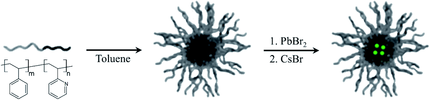 | ||
| Fig. 1 Schematic illustration of the preparation procedure of the PS-b-P2VP micelles with CsPbBr3 nanocrystals in the P2VP core. | ||
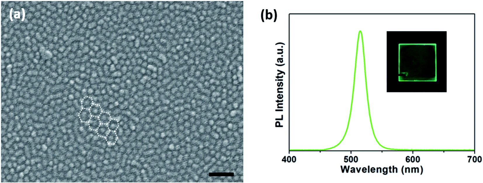
Upon the addition of CsBr into the micellar solution, we immediately observed green emission. The inset of Fig. 2a shows a green-emitting solution under UV illumination. The photoluminescence (PL) spectrum (solid line) from the solution has a maximum intensity at 515 nm with a full width at half maximum (FWHM) of 21 nm, which matches with the value in previous reports.6,32 It is noted that CsPbBr3 nanocrystals in PS-b-P2VP micelles showed the quantum yield of 51% and the fluorescence lifetime of 8 ns in the ref. 23. In the UV-Vis spectrum (dashed line), we can also find a characteristic absorption edge of CsPbBr3 near 510 nm. To confirm the formation of the CsPbBr3 nanocrystals, TEM images were obtained as shown in Fig. 2b. Micelles appear as dim gray spheres with blurred boundaries. Inside the micelles, however, we can distinguish 2–4 dark nanoparticles of ∼6 nm in diameter. We note that the hydrodynamic diameter of PS-b-P2VP micelles having CsPbBr3 nanocrystals by DLS is ∼69 nm (Fig. S1†). The high-resolution TEM image (inset of Fig. 2b) confirms the orthorhombic crystalline structure of the CsPbBr3 perovskite, where the measured values of 4.2 Å and 6.0 Å for d-spacing correspond to the (200) and (002) lattice planes, respectively. The size of the perovskite nanocrystals in the block copolymer micelles can be modified by adjusting the amount of perovskite precursor or by employing block copolymers with various molecular weights,29 which can affect the absorption and fluorescence properties of the perovskite nanocrystals.33
 | ||
| Fig. 2 PS-b-P2VP micelles having CsPbBr3 nanocrystals: (a) UV-Vis (dashed line) and fluorescence (solid line) spectra in a toluene solution with an excitation wavelength of 365 nm; (b) TEM image with a scale bar of 25 nm. The insets in (a) and (b) are a photograph of a green-emitting solution under UV illumination and a high-resolution TEM image of a single nanocrystal with dimensions of 15 nm × 15 nm, respectively. | ||
We can fabricate a film consisting of a monolayer of PS-b-P2VP micelles by adjusting the coating conditions. Fig. 3a shows an SEM image of a spin-coated monolayer of PS-b-P2VP micelles containing CsPbBr3 nanocrystals, in which the spherical micelles (∼42 nm in diameter) are arranged in a quasi-hexagonal order with an inter-particle distance of ∼55 nm without overlapping. A monolayer of micelles was also fabricated by dip-coating (Fig. S2†). As shown in the inset of Fig. 3b, we can observe uniform green fluorescence from a spin-coated monolayer on a quartz substrate. In the PL spectrum of this monolayer (Fig. 3b), the maximum intensity is located at 515 nm with a FWHM of 22 nm, identical to that from the micellar solution (Fig. 2a), implying that the micelles with CsPbBr3 nanocrystals were coated without deterioration.
 | ||
| Fig. 3 Spin-coated monolayer of PS-b-P2VP micelles having CsPbBr3 nanocrystals: (a) SEM image with the scale bar representing 200 nm; (b) fluorescence spectrum with an excitation wavelength of 365 nm. The inset in (b) shows a green-emitting film under UV illumination. | ||
In addition, we prepared a monolayer of PS-b-P2VP micelles having CsPbBr3 nanocrystals on a stretchable PDMS elastomer by spin-coating, which was confirmed by SEM (Fig. S3a†). As shown in Fig. 4, the micelle-coated PDMS elastomer exhibited green fluorescence, which was maintained under the extension of the elastomer. The fluorescence spectrum of the stretchable film (Fig. 4b) is almost identical to that of the monolayer film (Fig. 3). After recovered from extension, the elastomer still showed fluorescence without severe defects on the surface, presumably because the micelles arranged in the monolayer can be separated by extending their relative distance without being damaged during extension.34 The monolayer of micelles on the PDMS elastomer was preserved after extension without deterioration of the spherical shape of the micelles (Fig. S3b†). We note that the fluorescent PDMS elastomer coated with a monolayer of the micelles can be stretched up to ∼90% of its length before break.
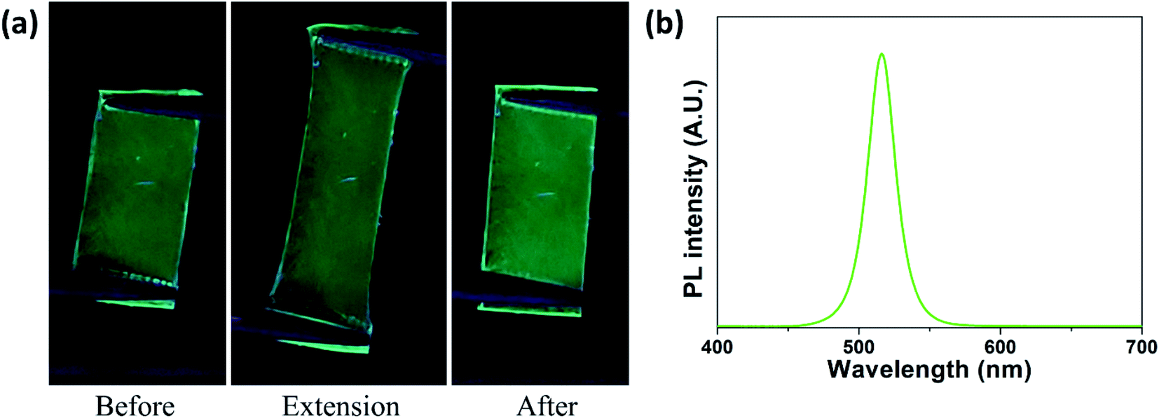 | ||
| Fig. 4 (a) Photographs of the stretchable PDMS elastomer coated with a monolayer of PS-b-P2VP micelles having CsPbBr3 nanocrystals under UV illumination before, during, and after extension; (b) fluorescence spectrum with an excitation wavelength of 365 nm. | ||
The emission color of the CsPbBr3 nanocrystals can be tuned by anion-exchange reactions.22 Fig. 5a shows micellar solutions with various fluorescence colors after treating the solution of PS-b-P2VP micelles having CsPbBr3 nanocrystals with ZnCl2 and ZnI2. With an increase in the amount of ZnCl2, the fluorescence color changed from green to light blue and then blue. In contrast, the emission turned into yellow and then red color with the addition of ZnI2. The PL spectra in Fig. 5b confirm variations in the emission color, in which the maximum intensity appears at 479 nm (light blue line) and 460 nm (blue line) after exchanging bromide with chloride and at 578 nm (yellow line) and 677 nm (red line) after anion exchange with iodide. It is noted that these PL spectra show relative intensities without normalization, and a PL spectrum of the green emission was obtained using a 1/3 diluted solution due to the high fluorescence intensity. We also note that the PL intensities highly decrease after anion-exchange reactions as reported in the literature.35 The decrease of PL intensities in perovskite nanocrystals after anion-exchange reactions is associated with deep trap states in the bandgap due to halide vacancies by different anion sizes.36,37
 | ||
| Fig. 5 Solutions of PS-b-P2VP micelles having CsPbBr3 nanocrystals after treatment with ZnCl2 or ZnI2: (a) photographs under UV illumination; (b) fluorescence spectra with an excitation wavelength of 365 nm. PL intensities in (b) are not normalized. For a PL spectrum of the green emission, a 1/3 diluted solution was used. | ||
Due to the weak fluorescence intensity from a monolayer of PS-b-P2VP micelles containing perovskite nanocrystals after anion exchange reactions, a film consisting of multilayered micelles was fabricated by lowering the spinning speed (1000 rpm) during spin-coating. Fig. 6 is an SEM image of the PS-b-P2VP micelles having CsPbBr3 nanocrystals on a Si substrate after spin-coating. From the top-view image, we can find that spherical micelles are preserved and randomly arranged overall, although a quasi-hexagonal arrangement can be locally observed. The side-view image (inset of Fig. 6) confirms that the film thickness (∼129 nm) is larger than the micelle diameter (∼42 nm), indicating a multilayer of micelles.
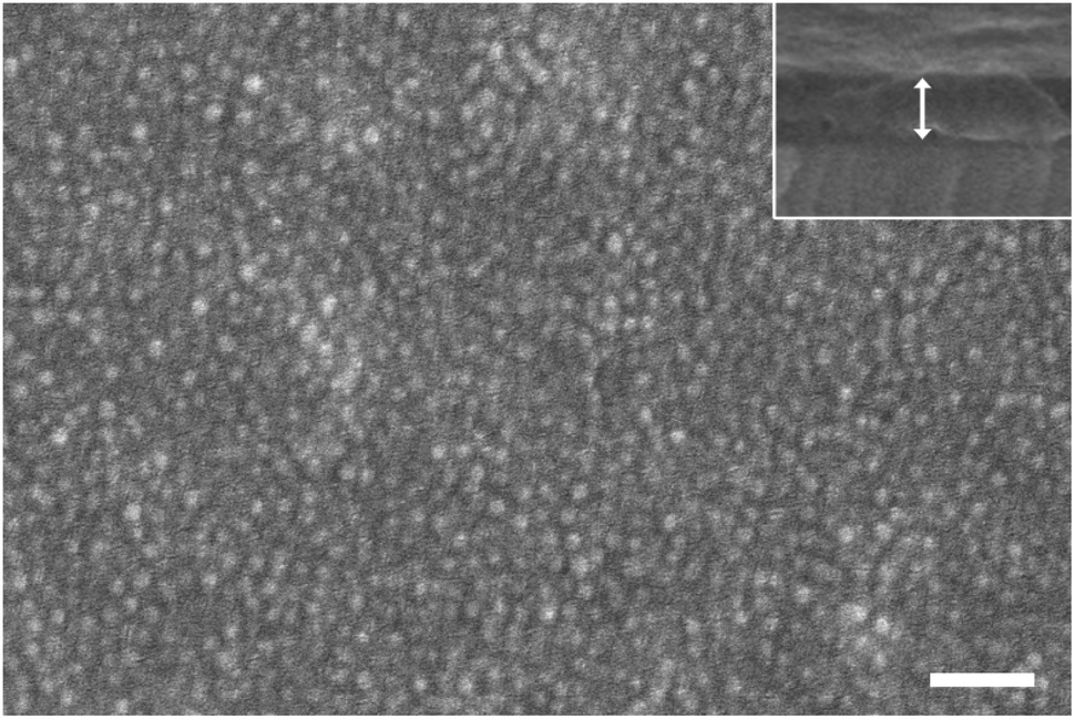 | ||
| Fig. 6 SEM image of a spin-coated film of PS-b-P2VP micelles having CsPbBr3 nanocrystals. The scale bar is 200 nm. The inset (400 nm × 300 nm) is a side view image of the film with the arrow indicating the thickness of ∼129 nm. | ||
A green-emitting film in Fig. 7 was obtained by the same procedure used to prepare the film shown in Fig. 6, with the exception of a flexible PET film as substrate. Because of the multilayered micelles having CsPbBr3 nanocrystals, the film exhibits much brighter fluorescence than the monolayer shown in the inset of Fig. 3b. In Fig. 7, we can also observe blue and red emissions from the films of multilayered micelles with perovskite nanocrystals after halide exchange reactions, which were prepared under the same spin-coating condition. As shown in the PL spectra given in the photographs, the maximum intensities of blue, green, and red emissions appear at 464 nm, 512 nm, and 660 nm, respectively. Each wavelength of the maximum intensity is almost same as that observed in a solution of the corresponding micelles. However, the fluorescence intensities of both red- and blue-emitting films were considerably lower than that of the green-emitting film as shown in the PL spectra given in the photographs. It is worthwhile to note that the emissions of all three colors are apparently unchanged from curved films as displayed in Fig. 7, presumably because the perovskite nanocrystals are imbedded in polymeric micelles.
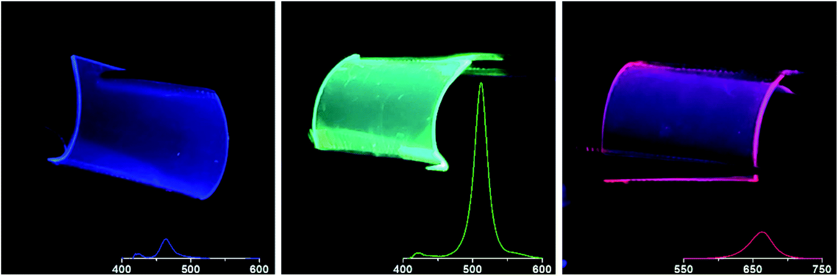 | ||
| Fig. 7 Photographs of flexible PET films coated with films of micelles having blue-, green-, and red-emitting perovskite nanocrystals. Fluorescence spectra are displayed together without intensity normalization. The excitation wavelength was 365 nm. | ||
Since fluorescent films in three primary colors of blue, green, and red can be produced as shown in Fig. 7, a white-emitting film can be expected with combination of PS-b-P2VP micelles containing perovskite nanocrystals. However, there were large variations in the PL intensities of the three colors so that it was necessary to adjust the thickness of each colored layer with a proper coating condition for reasonable white emission. A red-emitting film of micelles was first drop-casted from a thicker micellar solution (2.0 wt%) compared to a spin-coating solution (0.5 wt%). Then, green- and blue-emitting films of micelles were sequentially spin-coated onto the red-emitting film. A thicker solution (2.0 wt%) was also used for the blue-emitting film. It is noted that the thickness (∼18 μm) of the white-emitting film (Fig. S4†) was substantially larger than that (∼129 nm) of the green-emitting film (Fig. 6). After sequential coating of micelles having red-, green-, and blue-emitting perovskite nanocrystals, a PL spectrum of white emission was obtained as shown in Fig. 8, which has three maxima at 462, 517, and 673 nm. Each wavelength of the three maxima corresponds to that in the spectra of the individual films of three primary colors of perovskite nanoparticles. We note that this observation can be an evidence against halogen migration or segregation, which would be restricted by the stacked structure of the film as well as by the corona layer encompassing the nanocrystals. The polymeric parts in the film would suppress the diffusion of halogen anions associated with photo-induced charge carriers.24 The color coordinate of the spectrum is (0.29, 0.31) marked as a white dot in the CIE diagram (inset of Fig. 8), which is close to the white color of (0.31, 0.33). It is worthwhile to note that a white-emitting film is demonstrated with three primary colors from perovskite nanocrystals in polymeric micelles without other emissive materials.22,38 We also note that a decent choice of emission colors can be expected by adjusting the intensity of each color, based on the triangle mark with three color coordinates of blue, green, and red emissions of the spectrum (inset of Fig. 8).
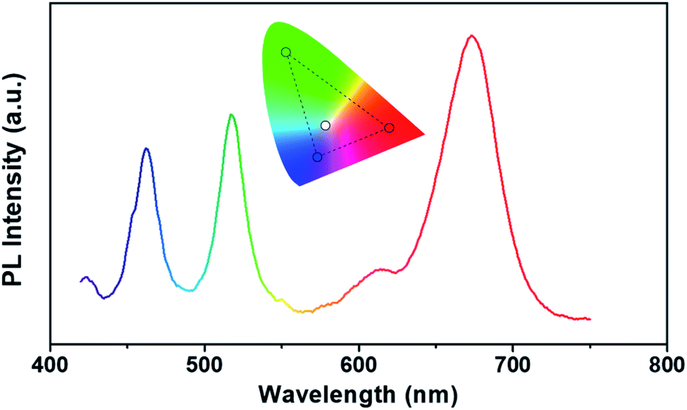 | ||
| Fig. 8 Fluorescence spectrum of a white-emitting film fabricated by sequential coating of micelles having red-, green-, and blue-emitting perovskite nanocrystals. The inset is a CIE chromaticity diagram with marks of blue (0.26, 0.15), green (0.11, 0.68), red (0.58, 0.30), and white (0.29, 0.31) colors from the film. The excitation wavelength was 400 nm. | ||
To fabricate a freestanding film of PS-b-P2VP micelles having perovskite nanocrystals without a supporting substrate, a film of the micelles was drop-casted and detached from the substrate. As shown in the inset of Fig. 9, a green-emitting film of ∼10 μm in thickness was separated from the substrate without discernible damage and was freely held. Freestanding films of blue and red emissions were also obtained by drop-casting. Although the films were immersed in water for longer than 30 min during the detaching process, there was no noticeable deterioration in emissions (Fig. 9), so that we intentionally submerged a green-emitting film in water (Fig. 10). After 30 min, the film well maintained green fluorescence (Fig. 9 and 10), indicating that the water-sensitive perovskite nanocrystals were protected by the hydrophobic polystyrene corona of the polymeric micelles.39 In addition, proper protection can apparently be obtained by favor of the film structure, in which polystyrene coronas overlap with each other, when the extremely low water permeability of polystyrene is considered.40
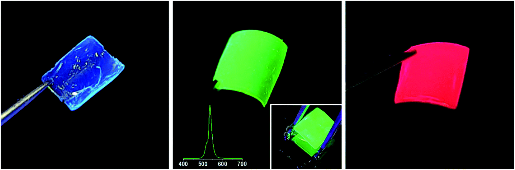 | ||
| Fig. 9 Photographs of the freestanding films of the PS-b-P2VP micelles having blue-, green-, and red-emitting perovskite nanocrystals under UV illumination. The inset shows a green-emitting film just after delamination from the substrate. A fluorescence spectrum of the green-emitting film with an excitation wavelength of 365 nm is displayed together in the photograph. | ||
 | ||
| Fig. 10 A freestanding film of the PS-b-P2VP micelles having green-emitting perovskite nanocrystals immersed in water under UV illumination. The right image shows a green-emitting film after 30 min in water. | ||
4. Conclusion
With the assistance of a well-established strategy of block copolymer micelles for nanoparticle synthesis, we proved the processability of perovskite nanocrystals by demonstrating stretchable, flexible, and self-supporting films independently. We first fabricated a stretchable fluorescent film by coating a monolayer of PS-b-P2VP micelles having CsPbBr3 nanocrystals on an elastomer. Then, after anion exchange reactions, we prepared flexible films of the micelles with perovskite nanocrystals showing three primary colors of blue, green, and red. Thus, by sequential coating of these micelles, we produced a white-emitting film in the color coordinates of (0.29, 0.31), which is close to the white color of (0.31, 0.33) in the CIE diagram, by all three primary colors from perovskite nanocrystals without the support of other kinds of emissive materials. In addition, a freestanding film of PS-b-P2VP micelles having perovskite nanocrystals without a supporting substrate exhibited stable fluorescence in water. Thus, the block copolymer micelle approach successfully allowed the processability of perovskite nanocrystals with adjustable fluorescence, which can be further applied to potential applications such as stretchable or flexible devices based on perovskite nanocrystals.Conflicts of interest
There are no conflicts of interest to declare.Acknowledgements
This research was supported by Basic Science Research Program through the National Research Foundation of Korea (NRF-2021R1A2C2003512).References
- A. K. Jena, A. Kulkarni and T. Miyasaka, Chem. Rev., 2019, 119, 3036 CrossRef CAS PubMed.
- Y. Zhao and K. Zhu, Chem. Soc. Rev., 2016, 45, 655 RSC.
- D. Yang, M. Cao, Q. Zhong, P. Li, X. Zhang and Q. Zhang, J. Mater. Chem. C, 2019, 7, 757 RSC.
- M. Jeong, I. W. Choi, E. M. Go, Y. Cho, M. Kim, B. Lee, S. Jeong, Y. Jo, H. W. Choi, J. Lee, J. H. Bae, S. K. Kwak, D. S. Kim and C. Yang, Science, 2020, 369, 1615 CrossRef CAS PubMed.
- X. X. Gao, W. Luo, Y. Zhang, R. Hu, B. Zhang, A. Züttel, Y. Feng and M. K. Nazeeruddin, Adv. Mater., 2020, 32, 1905502 CrossRef CAS PubMed.
- X. Du, G. Wu, J. Cheng, H. Dang, K. Ma, Y. W. Zhang, P. F. Tan and S. Chen, RSC Adv., 2017, 7, 10391 RSC.
- F. Zhang, H. Zhong, C. Chen, X. G. Wu, X. Hu, H. Huang, J. Han, B. Zou and Y. Dong, ACS Nano, 2015, 9, 4533 CrossRef CAS PubMed.
- D. Xing, C. C. Lin, Y. L. Ho, A. S. A. Kamal, I. T. Wang, C. C. Chen, C. Y. Wen, C. W. Chen and J. J. Delaunay, Adv. Funct. Mater., 2021, 31, 2006283 CrossRef CAS.
- S. Yakunin, L. Protesescu, F. Krieg, M. I. Bodnarchuk, G. Nedelcu, M. Humer, G. De Luca, M. Fiebig, W. Heiss and M. V. Kovalenko, Nat. Commun., 2015, 6, 8056 CrossRef CAS PubMed.
- Q. Chen, J. Wu, X. Ou, B. Huang, J. Almutlaq, A. A. Zhumekenov, X. Guan, S. Han, L. Liang, Z. Yi, J. Li, X. Xie, Y. Wang, Y. Li, D. Fan, D. B. L. Teh, A. H. All, O. F. Mohammed, O. M. Bakr, T. Wu, M. Bettinelli, H. Yang, W. Huang and X. Liu, Nature, 2018, 561, 88 CrossRef CAS PubMed.
- Q. Xu, J. Wang, W. Shao, X. Ouyang, X. Wang, X. Zhang, Y. Guo and X. Ouyang, Nanoscale, 2020, 12, 9727 RSC.
- Q. Dong, Y. Fang, Y. Shao, P. Mulligan, J. Qiu, L. Cao and J. Huang, Science, 2015, 347, 967 CrossRef CAS PubMed.
- C. Wehrenfennig, G. E. Eperon, M. B. Johnston, H. J. Snaith and L. M. Herz, Adv. Mater., 2014, 26, 1584 CrossRef CAS PubMed.
- V. A. Hintermayr, A. F. Richter, F. Ehrat, M. Döblinger, W. Vanderlinden, J. A. Sichert, Y. Tong, L. Polavarapu, J. Feldmann and A. S. Urban, Adv. Mater., 2016, 28, 9478 CrossRef CAS PubMed.
- L. Protesescu, S. Yakunin, M. I. Bodnarchuk, F. Krieg, R. Caputo, C. H. Hendon, R. X. Yang, A. Walsh and M. V. Kovalenko, Nano Lett., 2015, 15, 3692 CrossRef CAS PubMed.
- H. Huang, M. I. Bodnarchuk, S. V. Kershaw, M. V. Kovalenko and A. L. Rogach, ACS Energy Lett., 2017, 2, 2071 CrossRef CAS PubMed.
- J. Kang and L. W. Wang, J. Phys. Chem. Lett., 2017, 8, 489 CrossRef CAS PubMed.
- Q. A. Akkerman, G. Rainò, M. V. Kovalenko and L. Manna, Nat. Mater., 2018, 17, 394 CrossRef CAS PubMed.
- M. Lu, H. Wu, X. Zhang, H. Wang, Y. Hu, V. L. Colvin, Y. Zhang and W. W. Yu, ChemNanoMat, 2019, 5, 313 CrossRef CAS.
- H. Huang, B. Chen, Z. Wang, T. F. Hung, A. S. Susha, H. Zhong and A. L. Rogach, Chem. Sci., 2016, 7, 5699 RSC.
- T. Xuan, J. Huang, H. Liu, S. Lou, L. Cao, W. Gan, R. S. Liu and J. Wang, Chem. Mater., 2019, 31, 1042 CrossRef CAS.
- Y. J. Yoon, Y. Chang, S. Zhang, M. Zhang, S. Pan, Y. He, C. H. Lin, S. Yu, Y. Chen, Z. Wang, Y. Ding, J. Jung, N. Thadhani, V. V. Tsukruk, Z. Kang and Z. Lin, Adv. Mater., 2019, 31, 1901602 CrossRef PubMed.
- S. Hou, Y. Guo, Y. Tang and Q. Quan, ACS Appl. Mater. Interfaces, 2017, 9, 18417 CrossRef CAS PubMed.
- V. A. Hintermayr, C. Lampe, M. Löw, J. Roemer, W. Vanderlinden, M. Gramlich, A. X. Böhm, C. Sattler, B. Nickel, T. Lohmüller and A. S. Urban, Nano Lett., 2019, 19, 4928 CrossRef CAS PubMed.
- Y. Mai and A. Eisenberg, Chem. Soc. Rev., 2012, 41, 5969 RSC.
- S. K. Patra, R. Ahmed, G. R. Whittell, D. J. Lunn, E. L. Dunphy, M. A. Winnik and I. Manners, J. Am. Chem. Soc., 2011, 133, 8842 CrossRef CAS PubMed.
- W. Yan, X. Wan, Y. Xu, X. Lv and Y. Chen, Synth. Met., 2009, 159, 1772 CrossRef CAS.
- L. Tan and B. Tan, Chem. Soc. Rev., 2017, 46, 3322 RSC.
- X. Li, J. Iocozzia, Y. Chen, S. Zhao, X. Cui, W. Wang, H. Yu, S. Lin and Z. Lin, Angew. Chem., Int. Ed., 2018, 57, 2046 CrossRef CAS PubMed.
- S. S. Kim and B. H. Sohn, Carbon, 2016, 107, 124 CrossRef CAS.
- G. Kim, S. S. Kim, J. Jeon, S. I. Yoon, S. Hong, Y. J. Cho, A. Misra, S. Ozdemir, J. Yin, D. Ghazaryan, M. Holwill, A. Mishchenko, D. V. Andreeva, Y. J. Kim, H. Y. Jeong, A. R. Jang, H. J. Chung, A. K. Geim, K. S. Novoselov, B. H. Sohn and H. S. Shin, Nat. Commun., 2019, 10, 230 CrossRef PubMed.
- S. Jung, J. H. Kim, J. W. Choi, J. W. Kang, S. H. Jin, Y. Kang and M. Song, Nanomaterials, 2020, 10, 710 CrossRef CAS PubMed.
- A. O. El-Ballouli, O. M. Bakr and O. F. Mohammed, Chem. Mater., 2019, 31, 6387 CrossRef CAS.
- X. Yan, J. Yao, G. Lu, X. Li, J. Zhang, K. Han and B. Yang, J. Am. Chem. Soc., 2005, 127, 7688 CrossRef CAS PubMed.
- V. G. V. Dutt, S. Akhil and N. Mishra, CrystEngComm, 2020, 22, 5022 RSC.
- J. Ye, M. M. Byranvand, C. O. Martinez, R. L. Z. Hoye, M. Saliba and L. Polavarapu, Angew. Chem., Int. Ed., 2021, 60, 21636 CrossRef CAS PubMed.
- Q. A. Akkerman, V. D'Innocenzo, S. Accornero, A. Scarpellini, A. Petrozza, M. Prato and L. Manna, J. Am. Chem. Soc., 2015, 137, 10276 CrossRef CAS PubMed.
- S. Pan, Y. Chen, Z. Wang, Y. W. Harn, J. Yu, A. Wang, M. J. Smith, Z. Li, V. V. Tsukruk, J. Peng and Z. Lin, Nano Energy, 2020, 77, 105043 CrossRef CAS.
- Y. He, Y. J. Yoon, Y. W. Harn, G. V. Biesold-McGee, S. Liang, C. H. Lin, V. V. Tsukruk, N. Thadhani, Z. Kang and Z. Lin, Sci. Adv., 2019, 5, eaax4424 CrossRef CAS PubMed.
- S. Pauly, in Polymer handbook, ed. J. Brandrup, E. H. Immergut and E. A. Grulke, John Wiley & Sons, Inc., New York, 4th edn, 1999, vol. 1, pp. VI-568 Search PubMed.
Footnotes |
| † Electronic supplementary information (ESI) available. See DOI: 10.1039/d2ra00098a |
| ‡ Equal contribution. |
| This journal is © The Royal Society of Chemistry 2022 |