
 Open Access Article
 This Open Access Article is licensed under a Creative Commons Attribution-Non Commercial 3.0 Unported Licence
The impact of fluence dependent proton ion irradiation on the structural and optical properties of Bi5In30Se65 thin films for nonlinear optical devices
P. Priyadarshinia,
S. Dasa,
D. Alagarasanb,
R. Ganesanb,
S. Varadharajaperumalc,
S. Sahoode and
R. Naik *a
*a
aDepartment of Engineering and Material Physics, ICT-IOC, Bhubaneswar, 751013, India. E-mail: ramakanta.naik@gmail.com
bDepartment of Physics, Indian Institute of Science, Bangalore, 560012, India
cCentre for Nano Science and Engineering, Indian Institute of Science, Bangalore-560012, India
dLaboratory for Low Dimensional Materials, Institute of Physics, Bhubaneswar 751005, India
eHomi Bhabha Training School Complex, Anushakti Nagar, Mumbai 400094, India
First published on 9th February 2022
Abstract
This paper reports the effects of ion irradiation on the structural, linear, and nonlinear optical properties of thermally evaporated Bi5In30Se65 thin films. The prepared films were irradiated with 30 keV proton ions with different fluences, such as 5 × 10¹⁵ ions per cm2, 1 × 10¹⁶ ions per cm2, and 5 × 10¹⁶ ions per cm2. Structural analysis via X-ray diffraction (XRD) confirmed the non-crystalline nature of the film after ion irradiation with different doses. However, after the irradiation dose, the surface morphology changed, as shown by atomic force microscopy (AFM) images and field emission scanning electron microscopy (FESEM) images. The compositions of the films were obtained using energy-dispersive X-ray spectroscopy (EDX). Optical analysis via UV-Visible spectroscopy showed a reduction in the transmittance and an increase in the absorption in the higher wavelength region with irradiation. The optical bandgap and Tauc parameter decreased with an increase in the irradiation fluence, which is due to an increase in the irradiation-induced defects and disorder inside the system. The increases in the third order nonlinear susceptibility and the nonlinear refractive index with ion fluence are useful for nonlinear optical applications. The linear refractive index calculated from the transmittance data increased, satisfying Moss's rule. The optical parameters, such as lattice dielectric constant, optical density, skin depth, optical conductivity, real and imaginary dielectric constants, optical conductivity, loss factor, VELF, and SELF, were calculated using several empirical relationships and showed increasing behavior with the ion irradiation dose. The changes obtained in both the linear and nonlinear parameters will be useful for nonlinear optical device applications.
1. Introduction
Nowadays, the response of materials to intense external energy inputs such as thermal annealing,1,2 laser irradiation,3,4 ion irradiation,5,6 and doping7,8 to achieve the desired characteristics for fundamental studies and technological applications is gaining much attention. Among them, ion irradiation is one of the distinctive external energy input techniques that improve the structural and optical properties together with modification of the microstructural patterns of the system. These modifications are helpful when precisely designing the material properties required for the desired device applications. Several studies based on the consequences of the effects of ion irradiation have been carried out previously. The different doses of ion irradiation in Ge23Se62As15 thin films showed modifications of the surface morphology and optical properties which are useful for telecom and sensing applications.9 The ion implantation in Bi/GeSe2 films induces a significant alteration in the optical bandgap with the appearance of a topological Bi2Se3 phase in the structure.10 The proton irradiation of a Bi2Te3 film successfully enhances the defects' content, thus, enhancing the thermoelectric properties.11 These fascinating results from ion irradiation on various material characteristics have motivated the study of the ion irradiation impact on the films reported here.According to the energy transmitted through materials, the ion beams are divided into two categories such as low energy and high energy ion beams. The high energy ion beams possess energy ranging from a few tens of MeV to GeV that are carried by high atomic mass ions through inelastic collisions. The energetic ion beams with energy ranging from a few tens of keV to hundreds of keV are considered as low energy ion beams, generate defects and disorder in the system.12 Low energy ion beams basically interact with the target at the atomic level. After the bombardments of the target material, the accelerating incident ions experience a number of nuclear and electronic collisions. As a consequence of these elastic collisions, the ions lose all their energy and are implanted inside the target materials, thereby modifying several properties.13 Due to the elastic collisions, nuclear energy loss is more than electronic energy loss, and is mainly responsible for the material modification.14
In this regard, the Bi–In–Se films were considered the prototypical semiconducting materials with many useful applications. The high glass-forming ability of selenium and the presence of indium give the alloy photovoltaic properties, softness, and easy fusibility, and suitability for application purposes.15 After that, the addition of bismuth results in a considerable variation in linear and nonlinear optical properties as well as the structural phenomenon of the host system, in addition to carrier type reversal (CTR).16,17 For example, in addition to the CTR, the Bi doping also showed a large variation in the linear and nonlinear optical properties in the BixIn25−xSe75 thin films.18 The replacement of indium with bismuth provides a constant coordination number (Z = 2.25) that represented the structure in the floppy state which helps to determine the modifications in the network topology apart from the CTR behavior of the Bi–In–Se system.18,19 The modifications of several properties by varying the bismuth concentration in the BixIn35−xSe65 films results in the crystallinity of the highly Bi-doped films with a decrease in the optical bandgap.20 Until now there has been no relevant research on the impact of ion irradiation on Bi–In–Se thin films. So, in this study, we were interested in determining the outcome of the irradiation of low energy carried light ions, such as protons, on the Bi–In–Se thin film. Previously, the Bi5In30Se65 thin-film gained much attention because it showed the highest transmittance out of all the other BixIn35−xSe65 films, as well as showing an abrupt change in various linear and nonlinear optical parameters. Thus, in the present research, we were interested in studying the impact of ion irradiation on various structural, morphological, and optical linear and nonlinear properties of the Bi5In30Se65 thin-film with different fluences. Several studies have been performed on ion irradiation to demonstrate the tailoring of various characteristics of materials. For example, the effect of 80 MeV silicon swift heavy ion irradiation on the linear and nonlinear properties of the Ge24Se61Sb15 films makes them suitable for use in telecommunication and sensing applications.21 The ion irradiation, induced changes in the DC conductivity, and the electrical transport of the Ge20Se80−xBix films which is associated with the electronic energy loss of the ions inside the target material.22 With As–Se–Bi thin films, the use of 120 MeV Ag swift heavy ion irradiation, induced a decrease in the bandgap, and an increase in conductivity together with a p to n transition.23 The 3 MeV proton irradiation decreased the bandgap and increased the refractive index, dispersion energy in the amorphous-(Ge20Se80)0.96Ag0.04 thin films due to structural modification.24 The proton and deuteron irradiation changed the electronic conductivity under the influence of irradiation parameters and there was no change in the ionic conductivity of the quaternary Ag–Ge–As–S composite materials.25 The influence of proton beam irradiation over a Ge40Se60/Ag film stack reveals silver surface deposition and germanium oxidation, and a change in the film's chemistry as a result of proton irradiation.26 The electrical resistivity decreased with 10 MeV proton irradiation fluence in Cu(In,Ga)Se2 thin films which is due to the reduction of the concentration of the compensating donor-like defects, specifically the selenium vacancies.27
So, in the present study, the focus was on the proton irradiation-induced modifications in the structural, morphological, and optical properties of thermally evaporated Bi5In30Se65 thin films caused by different irradiation fluences. Because there was no previous significant research findings on the effect of ion implantation on the Bi–In–Se thin films, so as a first attempt, we were interested to expose the thin film to be irradiated by low energy proton ions with different fluences, which were precisely chosen to achieve a controllable performance. Thus, the change in properties was investigated at three different proton ion fluences: 5 × 10¹⁵ ions per cm2, 1 × 10¹⁶ ions per cm2, and 5 × 10¹⁶ ions per cm2 with low energy protons (30 keV) on Bi5In30Se65 thin films. The X-ray diffraction method (XRD) and atomic force microscope (AFM) were used to investigate the proton irradiation-induced structural alteration. The compositional analysis and surface morphological structure of the irradiated films were observed using energy-dispersive X-ray spectroscopy (EDX) attached to a field emission scanning electron microscope (FESEM). The UV-Vis spectroscopy was used for the optical study over the wavelength range of 450–1100 nm.
2. Experimental procedure
2.1 Sample preparation
The bulk glassy of highly pure Bi5In30Se65 was synthesized using the universal melt quenching procedure. Stoichiometric amounts of the high-purity elements Bi, In, and Se (99.999% Sigma-Aldrich) were weighed using an accurate sensitive balance, and then mixed inside a clean quartz ampoule evacuated under a pressure of 10−3 Torr. Then the ampoules were maintained in a high-temperature gradient at a heating rate of about 3–4 °C min−1 until 500 °C was reached inside the furnace and then that temperature was held for 20 h. These ampoules were frequently oscillated inside the furnace to confirm that the homogeneity of the molten mass had been obtained. Subsequently, the ampoules were taken out of the furnace and rapidly quenched in ice-cold water to avoid crystallinity. After that, the ampoules were broken and the bulk alloy was collected, and ground to give the powdered form.The homogeneous Bi5In30Se65 thin films of ∼800 nm thickness were achieved using the thermal evaporation method. To avoid air contamination inside the chamber, a vacuum coating unit (Hind-HiVac, Model 12A4D) was employed to create a vacuum atmosphere under 10−5 Torr pressure. Subsequently, a controllable deposition rate of 0.5 nm s−1 was maintained, whilst the Bi5In30Se65 chalcogenide vapor was deposited onto a cleaned glass substrate. Meanwhile, the deposition rate was monitored using a quartz crystal monitor. The substrate holder was rotated continuously to form a uniform and homogeneous film.
The prepared thin films were irradiated with 30 keV proton irradiation using a low energy ion implanter at Institute of Physics (IOP, Bhubaneswar, India). The proton irradiation was performed at three different fluences: 5 × 10¹⁵ ions per cm2, 1 × 10¹⁶ ions per cm2, and 5 × 10¹⁶ ions per cm2 under a high vacuum atmosphere (∼10−11 Torr) in the chamber. The ions were incident perpendicular to the sample surface. The desired ions (proton ions) were directed towards the sample by providing a certain voltage and current through a magnetic field. The ion beam was magnetically scanned over a 1 cm × 1 cm area covering the complete thin film surface that was fixed on a target ladder for uniform implantation and loaded inside the irradiation chamber. The ladder has the advantage of being able moving up and down which is controlled by a knob. The precisely controlled fluences and beam current were chosen by considering the time period and number of counts of the course of irradiation:
2.2 Sample characterization
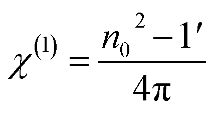
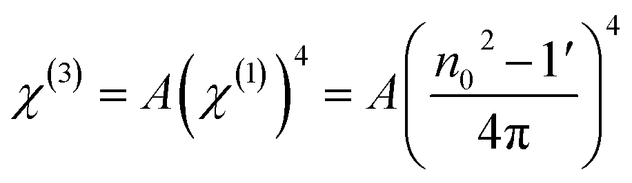
The structural characterizations of the proton irradiated Bi5In30Se65 film with different fluences were carried out by XRD (Bruker, D8 Advance) with a Cu Kα line (λ = 1.54 Å). The scanning range was 5°–80° at step size of 0.05° s−1 with a grazing angle of 1°. The irradiation induced topographic changes were investigated by AFM (APE Research, A-100). The modification in the elemental composition and surface morphological structure of the films due to irradiation was observed using a EDX spectrometer attached to an FESEM unit (Carl Zeiss, Ultra 55). The optical transmission data of the films were recorded by using a UV-Visible spectrophotometer (Syntronics, India, AU2702 over a 450–1100 nm range). The linear optical parameters, such as absorption coefficient (α), extinction coefficient (k), optical density (OD), and refractive index (n) were evaluated using the transmittance data. Likewise, the optical bandgap (Eg), and Tauc parameters (B1/2) were calculated from the Tauc relationship. The Dimirov and Sakka empirical relationship, and Miller's rule were implemented for the calculation of the static refractive index (n0), high-frequency dielectric constant (ε∞), and nonlinear parameters such as nonlinear susceptibility (χ(3)) and nonlinear refractive index (n2).3. Results and discussion
3.1 Structural analysis
| Sample | Se (keV nm−1) | Sn (keV nm−1) | Range (nm) | Longitudinal straggling (nm) | Lateral straggling (nm) |
|---|---|---|---|---|---|
| Bi–In–Se | 0.08693 | 0.00044 | 274.4 | 140.1 | 123.8 |
In Fig. 1(a), the electronic energy loss (Se) and the nuclear energy loss (Sn) are shown as a function of energy. The figure shows that the electronic energy loss is dominant over nuclear energy loss which agrees with results of other studies.28,29 The dominating nature of the Se indicates that the energy loss may ionize the target atoms, or excite the electrons of the target from the valence band (VB) to the conduction band (CB), or may result in a plasmonic effect which results in the alteration of several properties. The range of ions (274.4 nm) is within the range of the Bi5In30Se65 film thickness (∼800 nm). Thus, the ions easily penetrate through the film and become implanted in the thin films.
 | ||
| Fig. 1 (a) The SRIM simulation of Se Sn and the range (inset), and the (b) XRD patterns of 30 keV proton ion irradiated Bi5In30Se65 films at different fluences. | ||
 | ||
| Fig. 2 AFM images of the ion irradiated Bi5In30Se65 thin films. | ||
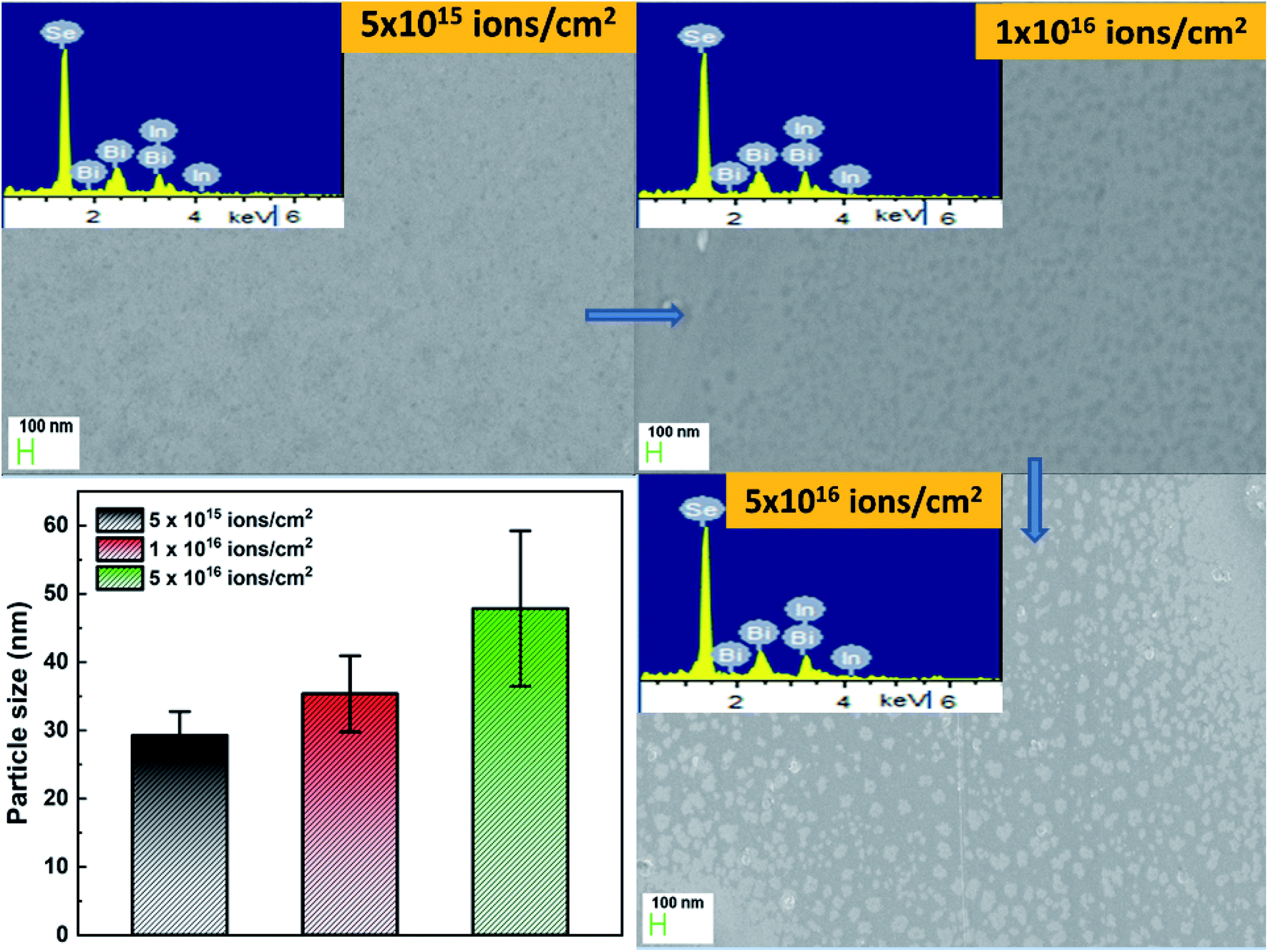 | ||
| Fig. 3 FESEM and EDX images and a particle size histogram of the ion irradiated Bi5In30Se65 thin films. | ||
| Sample | Bi5In30Se65 | |||
|---|---|---|---|---|
| 5 × 10¹⁵ ions per cm2 | 1 × 10¹⁶ ions per cm2 | 5 × 10¹⁶ ions per cm2 | ||
| Element | Calc. (at%) | Obs. (at%) | Obs. (at%) | Obs. (at%) |
| Se | 65 | 66.85 | 66.30 | 67.03 |
| In | 30 | 29.10 | 28.97 | 28.62 |
| Bi | 5 | 4.05 | 4.73 | 4.35 |
| Total | 100 | 100 | 100 | 100 |
The FESEM images at the scale of 100 nm are shown in Fig. 3, which clearly show the homogeneity and uniformity of the studied films. The 5 × 10¹⁶ ion irradiated film shows some granular structure which might be due to the ion irradiation. The films studied were of 1 × 1 cm2 shape with a film thickness of ∼800 nm deposited on a glass substrate. We have calculated the particle sizes for all irradiated films were calculated using ImageJ software (Java 1.8.0_172 version) and this software was also used for the statistical analysis shown in Fig. 3. The observed particle sizes were in range of 29.26 nm (5 × 10¹⁵ ions per cm2), 35.34 nm (1 × 10¹⁶ ions per cm2), 47.82 nm (5 × 10¹⁶ ions per cm2). It was observed that the particle size was enhanced with an increase in the ion irradiation dose which was also clearly seen from the FESEM image. However, there was no sign of any crystallinity from the XRD data. This enhancement in the particle size indicated that irradiation led to an enhancement of the concentration of large particles, and the disappearance of smaller particles with the formation of a granular structure. The results of the FESEM analysis confirmed that the grains covered the entire surface of the substrate. The appearance of a larger particle size will improve the performance of the solar cell, as the charge carriers encounter fewer trapping and scattering sources.30
3.2 Optical analysis
Transmittance (T) and reflectance (R). The optical properties of the material deal with the various phenomenon of light interactions with the material and the related modifications of the material's behavior. Thus, those properties are closely related to the material's atomic structure, electronic band structure, and electric properties. The optical behavior plays an important role in determining the applicability of the for use in optoelectronic devices.31,32 The optical transmittance (T) and reflectance (R) of different ion irradiated Bi–In–Se films are shown in Fig. 4(a) for the wavelength range of 450–1100 nm. The transmittance spectrum consisted of few numbers of distinct fringes over the visible to infrared region. The appearance of the fringes was caused by the interference phenomenon between light, the substrate, and the film interface medium.33 It was observed that the transmittance decreased with an increase in the ion irradiation fluence. This reduction in the transmittance behavior of the irradiated film was due to an increase in lattice defects and the creation of localized states within the VB and the CB.34 The absorption edge shifted to a higher wavelength region with an increase in the fluence.
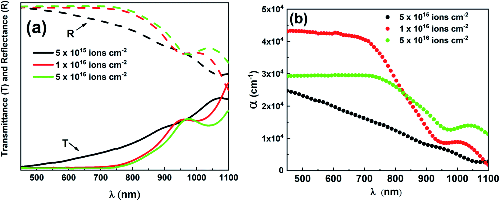 | ||
| Fig. 4 (a) The transmittance and reflectance, and (b) the absorption coefficients of the studied thin films. | ||
Absorption coefficient (α). The absorption coefficient (α) of the irradiated Bi5In20Se65 thin film was determined from the transmittance T(λ) and film thickness (d) by following formula:35
 | (1) |
Fig. 4(b) shows the spectral dependence of the absorption coefficient on the wavelength for the irradiated films. It was observed that the absorption coefficient decreased as the wavelength increased and in addition it also increased with the ion irradiation dose. The films possessed a large absorption coefficient of 104 cm−1 over the visible range which was in agreement with research reported in the literature.8,36
Extinction coefficient (k), optical bandgap (Eg), and Tauc parameter (B1/2). The extinction coefficient (k) or absorption index played an important role in the determination of several optical measurements which were related to the absorption of light waves in the medium, and the dielectric constants. This was related to the fraction of light that was scattered or absorbed over unit distance through the medium. The extinction coefficient k values were estimated by the formula:37
 . Fig. 5(a) shows the extinction coefficient as a function of incident energy for the proton irradiated thin films. The extinction coefficient primarily increased with energy, and then decreased with a higher energy value, which indicated that the film became more transparent at a higher energy. The lower value of k over a higher energy region represented the loss of light by scattering and absorption, whereas the propagation was decreased in the films studied. From this figure, it can be observed that the extinction coefficient k varies with the ion irradiation dose.
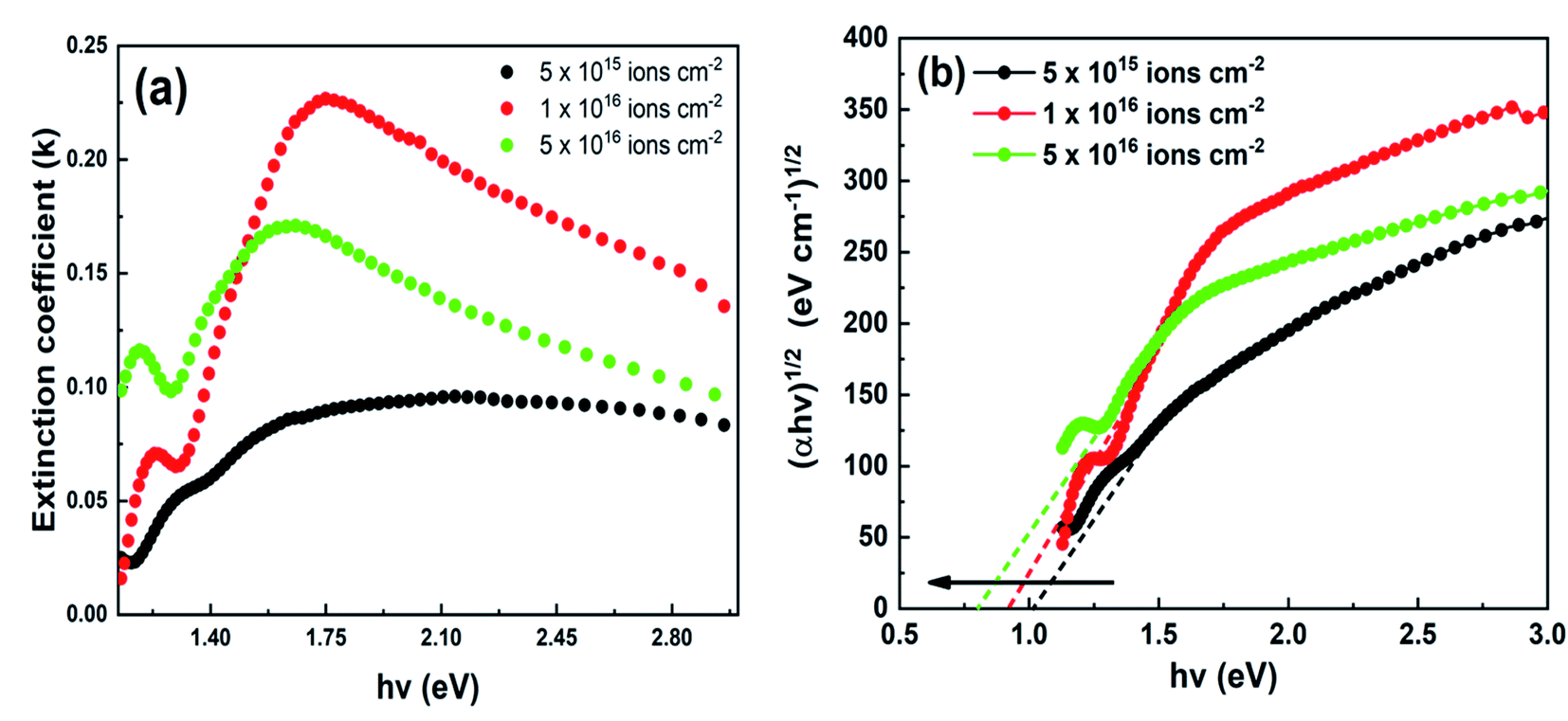 | ||
| Fig. 5 (a) Variation in extinction coefficient values and (b) (αhν)1/2 vs. hν plots of the proton irradiated thin films. | ||
The effective bandgap of the films studied was calculated from the Tauc relationship38 as given by:
| (αhv) = B(hv − Eg)p | (2) |
Using an organic poly(vinylpyrrolidone) (PVP) matrix doped with MoS2, quantum dots organic–inorganic hybrid nano-waveguides were developed, and then these were used as guides to obtain combined subwavelength field localization. Two different colors of light emissions at the nano-waveguide terminals were achieved due to self-absorption-related energy dissipation. The work was based on the organic PVP matrix doped with MoS2 quantum dots waveguide which showed the variation in PL intensity evolution, which occurred as the ∼575 nm shifted to 580 nm as the distance increased. This uniform and stable colorful emission could possibly be used in applications including optical routing in photonic circuits and devices, colorful displays, and output coupling of laser emissions.44 Similarly, high-quality hexagonal Cu2Te microdisks on copper foam were fabricated using chemical vapor deposition (CVD). This study showed PL at ∼627.5 nm and an enhancement in charge transfer and exciton resonance in surface enhanced Raman spectroscopy (SERS) detection showed the potential for its use in light-emitting diodes, lasers, and so on.45 As is already known, PL basically involves contributions from high-energy near band emission recombination and low-energy bands corresponding to deep level transitions (optical energy gap) and defects.46 These factors are very much responsible for the shifting of the PL spectra towards higher/lower wavelengths. In this case, the decrease of optical bandgap (1.01–0.79 eV) with an increase in defect density, and red shifting of the absorption edge (650–850 nm) was nearly close to the referred PL peak positions. Hence, the irradiated Bi5In30Se65 film may be a potential candidate for use as optical waveguides, red lasing, photonics, and biological detection of aromatic molecules, optical routing in photonic circuits and device applications.
Furthermore, the monolayer MoS2 with a low dimensional nanostructure shows potential for use in practical light-emitting applications. Here, the recent advances on the manipulations done in monolayer MoS2 by plasmonic nanostructures to obtain PL, and their possible applications in nanoscale photonics and optoelectronics are presented. The bandgap normalization of the MoS2 monolayer showed a high bandgap (∼2.19 eV) without photoexcitation, which was about 0.4 eV lower than that of the undoped MoS2 monolayer, and which showed environmental stability, high optical transparency, and PL spectra at ∼680 nm. These characteristics were also close to those of our irradiated films which showed optical transparency, a close absorption edge, and so on, meaning that the studied samples were useful for light generation, transmission, modulation, and detection applications.47
Refractive index (n), static refractive index (n0), and high-frequency dielectric constant (ε∞). The refractive index is considered as an essential optical parameter which plays an important role in designing optical devices, and also provides information on the local fields, polarization, and phase velocity of light in the propagating material. The corresponding absorption edge of the studied films occurred at 650–850 nm, thus the refractive index was calculated by using the transmittance obtained from the formula:48,49
 | (3) |
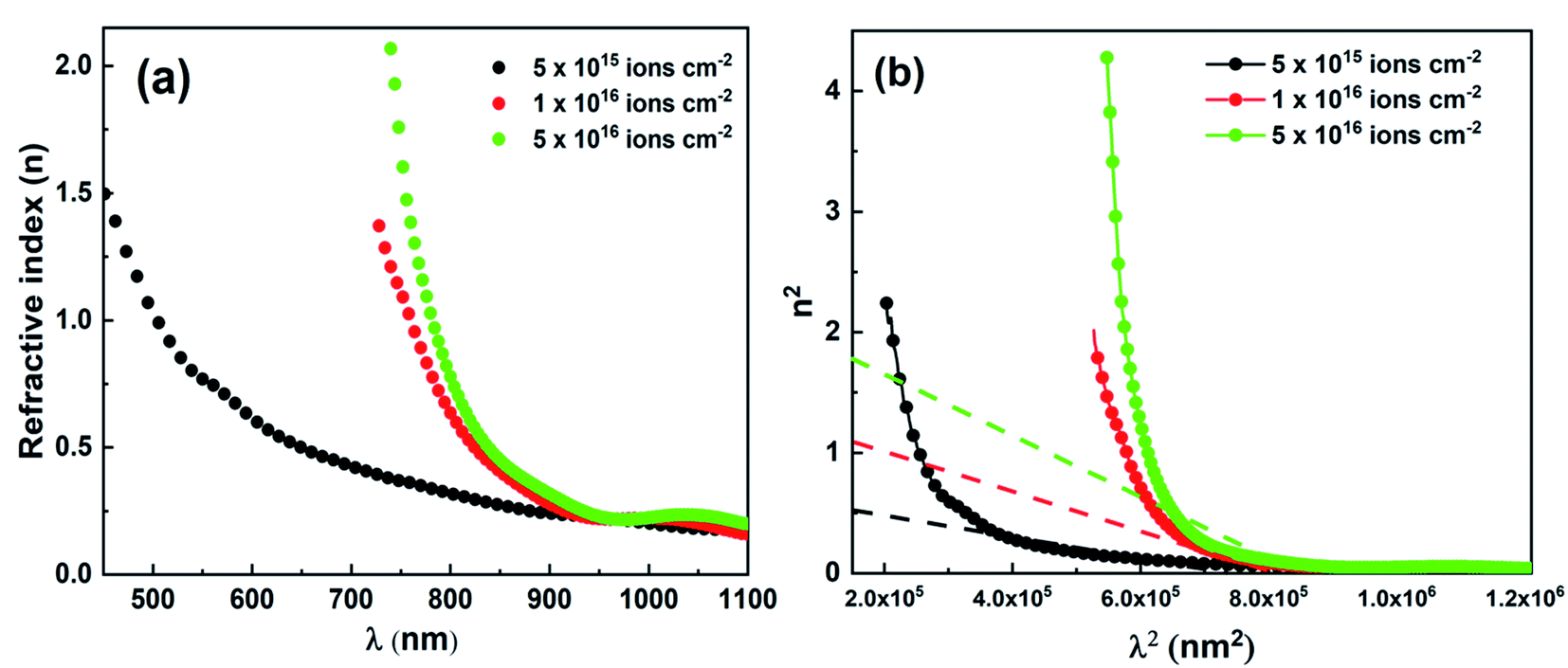 | ||
| Fig. 6 (a) The increase in the refractive index with fluence and (b) n2 vs. λ2 plots used to evaluate N/m* and ε∞. | ||
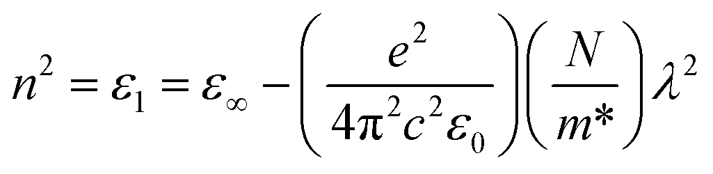
The static linear refractive index and high-frequency dielectric constant, ε∞ = n02 of the different ion irradiated Bi5In30Se65 films were calculated using the Dimitrov and Sakka relationship:53
 | (4) |
| Optical parameter | 5 × 10¹⁵ ions per cm2 | 1 × 10¹⁶ ions per cm2 | 5 × 10¹⁶ ions per cm2 |
|---|---|---|---|
| Optical bandgap (Eg) (eV) | 1.01 ± 0.02 | 0.93 ± 0.01 | 0.79 ± 0.02 |
| Tauc parameter (B1/2) (cm−1/2 eV−1/2) | 333 ± 3 | 321 ± 2 | 263 ± 2 |
| Static linear refractive index (n0) | 3.36 | 3.45 | 3.61 |
| High frequency dielectric constant of the lattice (ε∞ = n02) | 11.34 | 11.91 | 13.09 |
| Carrier concentration (N/m* × 1039) (kg−1 m−3) | 1.26 | 1.89 | 3.07 |
| Dielectric constant of the lattice, εL (from n2 vs. λ2 plot) | 0.69 | 1.35 | 2.15 |
| Optical electronegativity (ηOpt) | 1.65 | 1.64 | 1.62 |
| Plasma frequency (ωp2 × 1012) (Hz) | 1.30 | 1.00 | 1.03 |
| First-order non-linear susceptibility (χ(1)) | 0.82 | 0.86 | 0.96 |
| Third-order non-linear susceptibility (χ(3) × 10−10 esu) | 0.78 | 0.96 | 1.46 |
| Non-linear refractive index (n2 × 10−9 esu) | 0.87 | 1.05 | 1.52 |
High-frequency dielectric constant (ε∞) and carrier concentration (N/m*). The high-frequency dielectric constant (ε∞) and the ratio of carrier concentration per the effective mass (N/m*) can be estimated as follows:54
 | (5) |
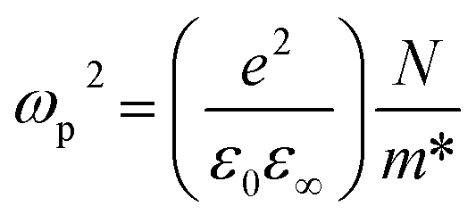
Plasma frequency (ωp), optical density (OD), and skin depth (δ). According to the Drude model, the plasma frequency (ωp) is a fundamental optical property which can be calculated by the formula:55
 | (6) |
The estimated plasma frequency value for the films studied is presented in Table 3. The ωp2 value showed an increment from 1.306 × 10¹² Hz to 1.008 × 10¹² Hz with the increase in the ion irradiation dose and then it slightly decreased to 1.032 × 10¹² Hz for the 5 × 10¹⁶ ion irradiated film. The change in the plasma frequency values indicated the change in the polarization process inside the system.56
The OD represents the measure of absorption loss of the incident radiation as it propagates through the materials. The OD can be estimated as,4 OD = α × d. Fig. 7(a) shows the estimated OD values with wavelength (λ). The figure shows that the OD showed the same pattern as the absorption coefficient, i.e., it increases with the ion irradiation doses. The absorbed energy in the material mostly depends on the extinction coefficient, type of material, and its conductivity and thickness over the absorption region. The absorbance percentage depends on the incident energy, which behaves exponentially when penetrating through the material system, which can be described by skin depth. Skin depth or penetration depth (δ) represents the path distance at which the incident radiation behaves exponentially with respect to the initial value. It is estimated from the reciprocal of the absorption coefficient (α),57 i.e., δ = 1/α. The skin depth variation with respect to energy (hν) is shown in Fig. 7(b). It was observed that the skin depth reduced to zero with an increase in energy. The height of these peaks was increased with the increase of the ion irradiation doses from 5 × 10¹⁵ ions per cm2 to 1 × 10¹⁶ ions per cm2 and then decreases with an ion irradiation dose of 5 × 10¹⁶ ions per cm2.
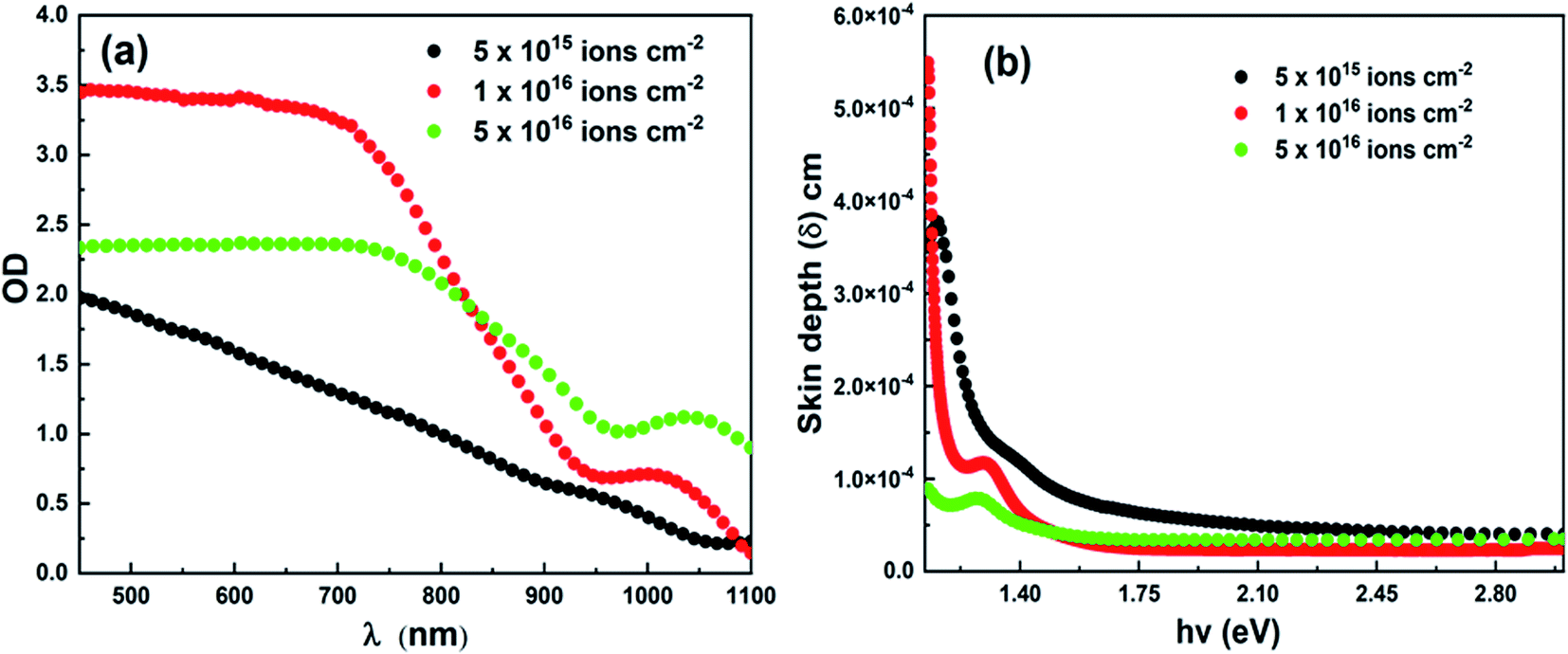 | ||
| Fig. 7 (a) The optical density and (b) the skin depth variation of the thin films under different fluences. | ||
Dielectric constants, loss factor, and quality factor. The dielectric constant is another important characteristic of the material that can be expressed as the real and imaginary dielectric constants. It basically relates the permittivity and polarizability of the material with the density of states within the forbidden energy gap region. The real part of the dielectric constant provides information about the slowdown of the speed of light when traversing through the material, whereas the respective imaginary part gives information about the absorption of energy by an electric field due to dipole motion. The values obtained for the refractive index and extinction coefficient have been used to evaluate the real (εr) and imaginary (εi) dielectric constants of the irradiated Bi5In30Se65 thin films by the expressions:58
| ε = εr + iεi = (n + ik)2 | (7) |
Fig. 8(a) and (b) show the wavelength dependence of the real and imaginary parts of the dielectric constant. It has been observed that both the estimated values, εi and εr increase with the ion irradiation dose. The imaginary dielectric constant had a lower value compared to the real dielectric constant which was mainly due to the low extinction coefficient values.
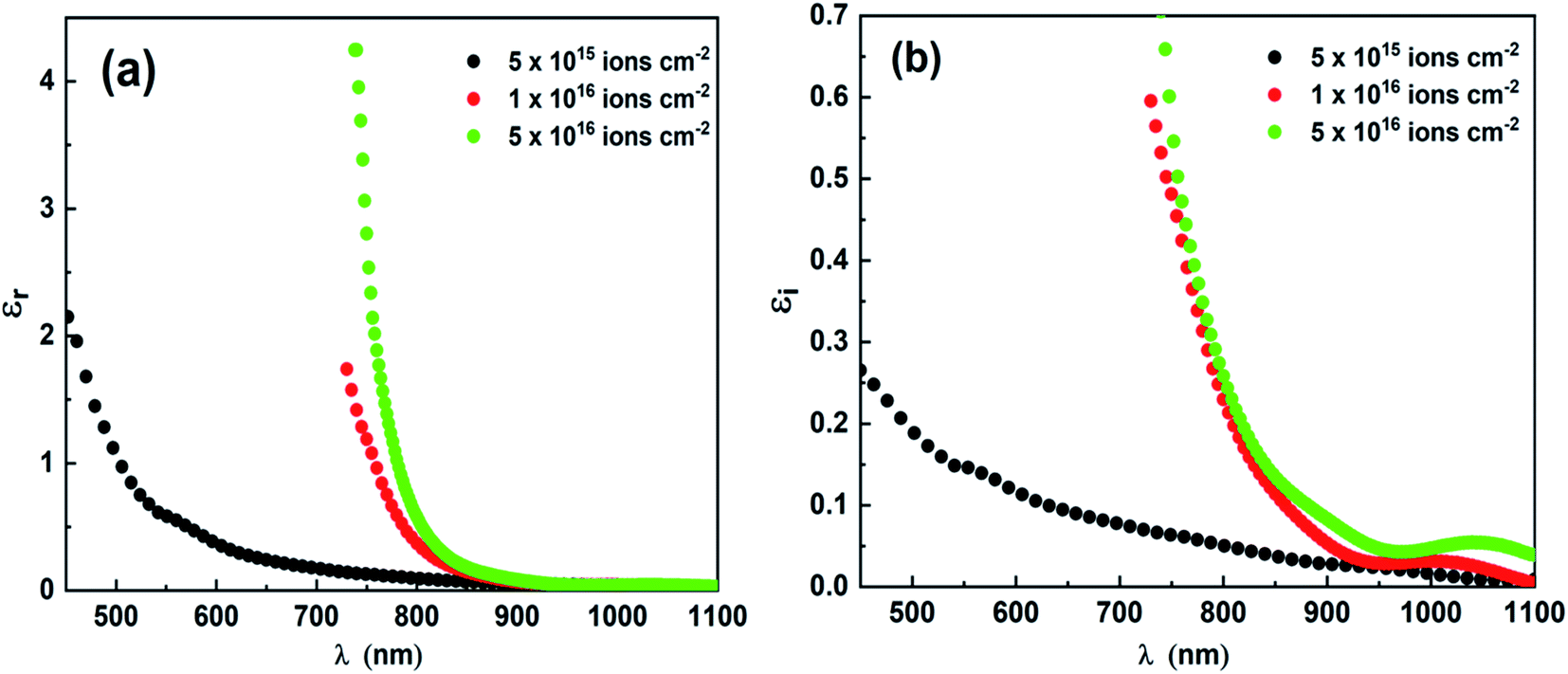 | ||
| Fig. 8 (a) εr plots and (b) εi plots of the proton irradiated Bi5In30Se65 thin films. | ||
The dielectric loss factor represents the loss rate of the power dissipated by the motion of charges through the electromagnetic field. It basically depends on the real and imaginary dielectric constants and is defined as,59 loss factor (tan![[thin space (1/6-em)]](https://www.rsc.org/images/entities/char_2009.gif) δ) = εi/εr. Similarly, the reciprocal of the dissipation factor represents the quality factor given by quality factor = 1/tanδ = εr/εi.
δ) = εi/εr. Similarly, the reciprocal of the dissipation factor represents the quality factor given by quality factor = 1/tanδ = εr/εi.
The spectral variations of the loss factor and the quality factor are shown in Fig. 9(a) and (b). It can be seen that at a lower wavelength region, the dielectric loss tangent has a low value and then increases with the increase in wavelength. The increase in ion irradiation dose increases the energy losses. Similarly, the quality factor showed a reduction with wavelength and the corresponding peak slightly shifted to a higher wavelength with higher ion irradiation doses.
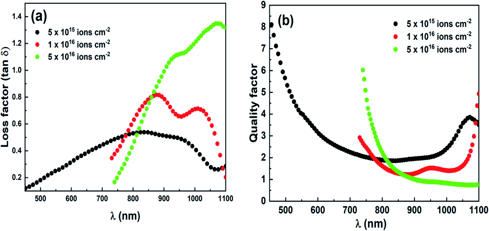 | ||
| Fig. 9 (a) Loss factor and (b) quality factor plots of the proton irradiated Bi5In30Se65 thin films. | ||
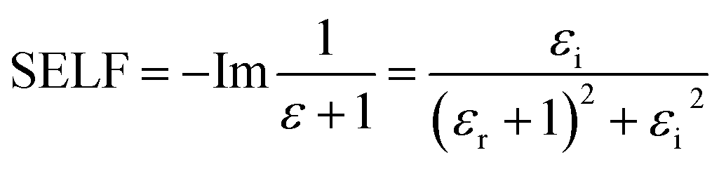
Volume and surface energy loss functions (VELF and SELF). When the energetic electrons pass throughout the thin film they lose energy due to the free electron density of the material. This characteristic energy loss is expressed by two parameters, i.e., volume energy loss function and surface energy loss function, which can be calculated as follows:60
 | (8) |
 | (9) |
Fig. 10(a) and (b) show the spectral dependence of VELF and SELF on the wavelength range of the irradiated thin films. It was observed that both SELF and VELF primarily increased with wavelength, and then decreased as the wavelength reached a higher value. The VELF was higher than SELF for the films studied in this research. This behavior was predictable in the case of semiconductor films, because the charge carriers suffer more collisions during the course of penetration through the bulk material. Also, increases in both VELF and SELF with ion irradiation doses could be due to an increase in defects and disorder which causes an increase in the collisions of the carrier during its journey through the material.61
 | ||
| Fig. 10 (a) VELF and (b) SELF plots of the proton irradiated Bi5In30Se65 thin films. | ||
Optical conductivity (σ). The optical conductivity in semiconductors showed an optical response with the incident light of the samples studied. This can be shown by the sum of real optical conductivity (σr) and imaginary optical conductivity (σi) that depended on the real and imaginary dielectric constants, given by:62
| σOpt = σr(ω) + iσi(ω), | (10) |
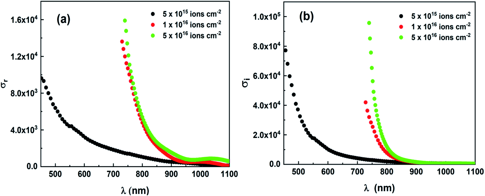 | ||
| Fig. 11 (a) Real and (b) imaginary optical conductivity plots of the proton irradiated films. | ||
Third-order nonlinear susceptibility (χ(3)) and nonlinear refractive index (n2). The nonlinear optical parameters are very important in the field of optoelectronic applications. This comes in to play when the intensity of incident radiation is sufficiently high that it can alter the properties of the materials. The linear optical susceptibility χ(1) for the thin films studied was evaluated using the following formula:63
 | (11) |
Furthermore, according to Miller's rule,64 third-order nonlinear susceptibility (χ(3)) can be evaluated from the linear optical susceptibility (χ(1)) as follows:
 | (12) |
Finally, the optical nonlinearities observed in this study showed enhanced values for the Bi5In30Se65 film compared to the previously reported data. Several physical phenomena could also be responsible for such observed high nonlinearity, such as the band gap shifting, the presence of highly polarizable Bi, and the presence of lone pair electrons in the chalcogenide Se atoms that can be easily polarized. This resulted in the homogenization and formation of highly polymerized covalent bonds inside the amorphous matrix as a consequence of the ion irradiation.65
The behavior of the nonlinear susceptibility and optical bandgap with respect to the ion irradiation doses is shown in Fig. 12. The increase in the nonlinear susceptibility may be due to the enhanced irradiation induced interactions between the fragments which increased the polymerization and homogenization inside the material, that then enhanced the susceptibility.71
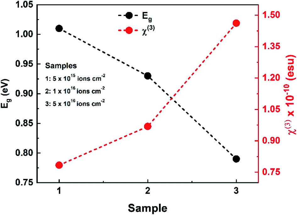 | ||
| Fig. 12 The variation of χ(3) and Eg with the ion irradiation dose for the studied thin films. | ||
In addition, the nonlinear refractive index, n2 of the investigated films were evaluated using Ticha and Tichy, and Miller's rule given by:72
 | (13) |
The value of the nonlinear refractive index obtained is given in Table 3. The nonlinear refractive index increased with the ion irradiation doses which was due to the increase of irradiation induced defect states that increased the local polarizability.73 The high value of the nonlinear refractive index indicated that the films studied could be interesting candidates for nonlinear optical applications. The nonlinear optical index, n2, of Ge10AsxTe90−x films, observed from an experimental Z-scan technique, showed a maximum index value of 4.96 × 10⁻¹³ esu, which was much lower than our observed nonlinear index value.74 Irradiation of 80 MeV silicon swift heavy ions on a Ge24Se61Sb15 thin film resulted in an increase in the n2 value from 1.7 × 10⁻¹⁰ esu to 2.6 × 10⁻¹⁰ esu, with an increase in ion fluence which also agreed with results in our study.21 These increases in nonlinear susceptibility and refractive index were due to the polarization dependent nature. The ion irradiation enhanced the polarizability of the material. The tailoring of the nonlinear optical properties of the Bi2Se3 film by ion irradiation showed a dependency on the irradiation-induced structural changes, i.e., relative atom displacement (RAD).75 This irradiation-induced structural modification was observed using Q-switched waveguide laser emission where the Bi2Se3 film acted as a passive absorber. In this case, the observed tailoring of the optical nonlinearity was correlated with the bandgap energy and other optical parameters, which can be used for various optical applications.
Optical electronegativity (ηOpt). Furthermore, the optical electronegativity, ηOpt that represents the ability of the positive radicals of atoms to attract the electrons of the same material to form ionic bonds could be evaluated according to Duffy, by using the static refractive index as follows:76
 | (14) |
4. Conclusions
The study reported here shows the effects of 30 keV proton ion irradiation on Bi5In30Se65 thin films at three different fluences: 5 × 10¹⁵ ions per cm2, 1 × 10¹⁶ ions per cm2, and 5 × 10¹⁶ ions per cm2. The XRD analysis showed the amorphous nature of the irradiated films. The change in surface structure was clearly seen from FESEM and AFM images. The transmittance decreased with irradiation, whereas the absorption coefficient increased with irradiation. The irradiation induced reduction of the optical bandgap with the ion irradiation dose is explained via the Mott and Davis model. Increases in the optical density, extinction coefficient, refractive index, real and imaginary dielectric constant, loss factor, VELF, SELF, and skin depth behavior were observed with an increase in the irradiation fluence. The static linear refractive index and high-frequency dielectric constants increased with irradiation. The optical electronegativity decreased with fluence, whereas the real and imaginary parts of the optical conductivity increased with the ion fluence. The third-order nonlinear susceptibility and nonlinear refractive index increased as a consequence, which indicates an increase in polarizability in the local structure. The large nonlinear susceptibility of the material enables it to be a good candidate for use in the manufacture of nonlinear optical devices.Data availability
The data that support the findings of this study are available from the corresponding author upon reasonable request.Author contributions
P. Priyadarshini: writing – original draft, software, experiments, data curation, investigation.S. Das: investigation, experiments.
S. Sahoo: visualization, experiments.
D. Alagarasan: investigation, experiments.
S. Vardharajaperumal: experiments.
R. Ganesan: visualization, investigation.
R. Naik: conceptualization, methodology, writing – review and editing, supervision.
Conflicts of interest
The authors declare that they have no known competing financial interests or personal relationships that could have appeared to influence the work reported in this paper. There are no conflicts of interest relating to this manuscript.Acknowledgements
R. Naik thanks the Department of Physics, Indian Institute of Science (IISc) for assistance with the optical and FESEM measurements.References
- J. A. Frantz, A. Clabeau, J. D. Myers, R. Y. Bekele, V. Q. Nguyen and J. S. Sanghera, Opt. Express, 2020, 28(23), 34744–34753 CrossRef CAS PubMed.
- D. Alagarasan, S. Varadharajaperumal, K. D. A. Kumar, R. Naik, A. Arunkumar and R. Ganesan, Optimization of different temperature annealed nanostructured CdSe thin film for photodetector applications, Opt. Mater., 2021, 122, 111706 CrossRef.
- L. Pan, B. Song, N. Mao, C. Xiao, C. Lin and P. Zhang, Optical properties of Ge-Sb-Se thin films induced by femtosecond laser, Opt. Commun., 2021, 496, 127123 CrossRef CAS.
- D. Sahoo, P. Priyadarshini, R. Dandela, D. Alagarasan, R. Ganesan, S. Vardharajperumal and R. Naik, In situ laser irradiation: the kinetics of the changes in the nonlinear/linear optical parameters of As50Se40Sb10 thin films for photonic applications, RSC Adv., 2021, 11(26), 16015–16025 RSC.
- P. Sharma, M. Vahistha, V. Ganesan and I. P. Jain, Ion irradiation-induced modifications in the surface morphology of Ge20Se74Bi6 thin films, J. Alloys Compd., 2008, 462, 452–455 CrossRef CAS.
- R. Panda, S. A. Khan, U. P. Singh, R. Naik and N. C. Mishra, The impact of fluence dependent 120 MeV Ag swift heavy ion irradiation on the changes in structural, electronic, and optical properties of AgInSe2 nano-crystalline thin films for optoelectronic applications, RSC Adv., 2021, 11(42), 26218–26227 RSC.
- A. El-Denglawey, V. Sharma, E. Sharma, K. A. Aly, A. Dahshan and P. Sharma, Optical and mechanical properties of Ag doped thermally evaporated SeTe thin films for optoelectronic applications, J. Phys. Chem. Solids, 2021, 159, 110291 CrossRef CAS.
- M. Behera, R. Naik, C. Sripan, R. Ganesan and N. C. Mishra, Influence of Bi content on linear and nonlinear optical properties of As40Se60−xBix chalcogenide thin films, Curr. Appl. Phys., 2019, 19, 884–893 CrossRef.
- S. Pandey and R. Chauhan, Contribution of 80 MeV silicon swift heavy ion irradiation for reforming of optical and structural properties of amorphous Ge23Se62As15 thin films for telecommunication and sensing applications, J. Non-Cryst. Solids, 2021, 554, 120597 CrossRef CAS.
- A. Aparimita, R. Naik, S. Sahoo, C. Sripan and R. Ganesan, Influence of low energy Ag ion irradiation for formation of Bi2Se3 phase from Bi/GeSe2 heterostructure thin films, Appl. Phys. A, 2020, 126, 203 CrossRef CAS.
- G. Goo, G. Anoop, S. Unithrattil, W. S. Kim, H. J. Lee and J. K. Jo, Proton-Irradiation Effects on the Thermoelectric Properties of Flexible Bi2Te3/PEDOT: PSS Composite Films, Adv. Electron. Mater., 2019, 5, 1800786 CrossRef.
- D. K. Avasthi and G. K. Mehta, Materials Engineering with Swift Heavy Ions, Springer Netherlands, 2011 Search PubMed.
- L. Thome, A. Debelle, F. Garrido and S. Mylonas, et al., Radiation effects in nuclear materials: Role of nuclear and electronic energy losses and their synergy, Nucl. Instrum. Methods Phys. Res., Sect. B, 2013, 307, 43–48 CrossRef CAS.
- Y. Zhang, T. Varga, M. Ishimaru, P. D. Edmondson, H. Xue, P. Liu, S. Moll, F. Namavar, C. Hardiman, S. Shannon and W. J. Weber, Competing effects of electronic and nuclear energy loss on microstructural evolution in ionic-covalent materials, Nucl. Instrum. Methods Phys. Res., Sect. B, 2014, 327, 33–43 CrossRef CAS.
- S. Jost, F. Hergert, R. Hock, J. Schulze, A. Kirbs, T. Vob and M. Purwins, The formation of CuInSe2 thin film solar cell absorbers from electroplated precursors with varying selenium content, Sol. Energy Mater. Sol. Cells, 2007, 91, 1669–1675 CrossRef CAS.
- A. Aparimita, M. Behera, C. Sripan, R. Ganesan, S. Jena and R. Naik, Effect of Bi addition on the optical properties of Ge30Se70−xBix thin films, J. Alloys Compd., 2018, 739, 997 CrossRef CAS.
- R. K. Pan, H. Z. Tao, H. C. Zang, X. J. Zhao and T. J. Zhang, Optical properties of pulsed laser deposited amorphous (GeSe2)100−xBix films, Appl. Phys. A, 2010, 99, 889–894 CrossRef CAS.
- S. Sharma, P. Kumar and R. Thangaraj, Effect of Bi additive on structure and optical properties of amorphous BixIn25−xSe75 chalcogenide films, Curr. Appl. Phys., 2013, 13, 731–735 CrossRef.
- R. P. Tripathi, M. A. Alvi and S. A. Khan, Investigations of thermal, optical and electrical properties of Se85In15−xBix glasses and thin films, J. Therm. Anal. Calorim., 2020, 146, 2261–2272 CrossRef.
- P. Priyadarshini, S. Das, D. Algarasan, R. Ganesan, S. Varadharajaperumal and R. Naik, Role of bismuth incorporation on the structural and optical properties in BixIn35−xSe65 thin films for photonic applications, J. Am. Ceram. Soc., 2021, 104(11), 5803–5814 CrossRef CAS.
- S. Pandey and R. Chauhan, Optical and structural modification in amorphous Ge24Se61Sb15 thin films under 80 MeV Silicon swift heavy ions for telecom and optical applications, Opt. Mater., 2021, 111, 110686 CrossRef CAS.
- P. Sharma, M. Vashistha and P. Jain, Electrical conductivity of ion irradiated Ge20Se80−xBix thin films, Radiat. Meas., 2003, 36, 663–666 CrossRef CAS.
- M. Behera, N. C. Mishra and S. A. Khan, Influence of 120 MeV Ag Swift Heavy Ion Irradiation on the optical and electronic properties of As-Se-Bi chalcogenide thin films, J. Non-Cryst. Solids, 2020, 544, 120191 CrossRef CAS.
- S. K. Tripathi, A. Thakur, G. Singh, J. Sharma, V. Sharma, K. P. Singh, G. S. S. Saini and N. Goyal, Proton-induced changes on the optical parameters of a-(Ge20Se80)0.96Ag0.04 thin films, J. Mater. Sci., 2006, 41, 1847–1850 CrossRef CAS.
- K. V. Kurochka, N. V. Melnikova, D. O. Alikin and T. E. Kurennykh, Irradiation effect on the structural and electrical properties of the glassy Ag-Ge-As-S composite material containing carbon nanotubes, Solid State Ionics, 2019, 341(5), 115026 CrossRef CAS.
- T. Nichol, G. Nagy, R. Huszank and D. Tenne, Proton beam effects on Ge–Se/Ag thin films, Phys. Status Solidi B, 2018, 255(6), 1700453 CrossRef.
- B. Koo, J. H. Lee, D. Shin, B. T. Ahn and B. Shin, Photoluminescence study of high energy proton irradiation on Cu (In,Ga)Se2 thin films, Thin Solid Films, 2016, 603, 134–138 CrossRef CAS.
- S. K. Sahoo, S. Mangal, D. K. Mishra, P. Kumar and U. P. Singh, Effect of low energy proton beam irradiation on structural and electrical properties of ZnO:Al thin films, Mater. Sci. Semicond. Process., 2017, 63, 76–82 CrossRef CAS.
- A. V. Krasheninnikov and K. Nordlund, Ion and electron irradiation-induced effects in nanostructured materials, J. Appl. Phys., 2010, 107, 071301 CrossRef.
- C. Bo, M. Yang, X. Zheng, W. Li, K. Zhu and S. Priya, Impact of capacitive effect and ion migration on the hysteretic behavior of perovskite solar cells, J. Phys. Chem. Lett., 2015, 6, 4693–4700 CrossRef PubMed.
- R. M. Hassan, A. Z. Mahmoud, M. A. Abdel-Rahim, H. S. Assaedi, S. W. Alraddadi and A. M. Abd-Elnaiem, Effect of thermal annealing on structure and optical properties of amorphous As30Te64Ga6 thin films, J. Inorg. Organomet. Polym., 2021, 31, 3037–3053 CrossRef CAS.
- B. K. Yadav, P. Singh, C. P. Yadav and D. K. Pandey, Synthesis and characterization of ZnSe1−xTex thin films, Phase Transform., 2021, 94, 326–337 CrossRef CAS.
- S. A. Gad, H. Shaban, B. A. Mansour and G. M. Mahmoud, Determination and analysis of linear and nonlinear optical properties and electrical conductivity of amorphous PbxGe42−xSe48Te10 thin films, Appl. Phys. A: Mater. Sci. Process., 2020, 26, 354 CrossRef.
- E. R. Shaaban, Y. A. M. Ismail and H. S. Hassan, Compositional dependence of the optical properties of amorphous Se80−xTe20Bix thin films using transmittance and reflectance measurements, J. Non-Cryst. Solids, 2013, 376, 61–67 CrossRef CAS.
- R. Naik, C. Sripan and R. Ganesan, Photo darkening in As50Se50 thin films by 532 nm laser irradiation, Opt. Laser Technol., 2017, 90, 158–164 CrossRef CAS.
- M. R. Balboul, Optical effects induced by gamma and UV irradiation in chalcogenide glass, Radiat. Meas., 2008, 43, 1360–1364 CrossRef CAS.
- A. A. A. Darwish, M. Rashad, A. E. Bekheet and M. M. El-Nahass, Linear and nonlinear optical properties of GeSe2−xSnx (0 ≤ x ≤ 0.8) thin films for optoelectronic applications, J. Alloys Compd., 2017, 709, 640–645 CrossRef CAS.
- J. Tauc, Amorphous and Liquid Semiconductors, Plenum Press, New York, 1979 Search PubMed.
- P. Priyadarshini, S. Das, D. Alagarasan, R. Ganesan, S. Vardharajperumal and R. Naik, Observation of high nonlinearity in Bi doped BixIn35−xSe65 thin films with annealing, Sci. Rep., 2021, 11, 21518 CrossRef CAS PubMed.
- K. Senthil, D. Mangalaraj, S. K. Narayandass, B. Hong, Y. Roh, C. S. Park and J. Yi, Argon and nitrogen implantation effects on the structural and optical properties of vacuum evaporated cadmium sulphide thin films, Semicond. Sci. Technol., 2002, 17, 97 CrossRef CAS.
- N. F. Mott and E. A. Davis, Electronics Processes in Non-crystalline Materials, Clarendon, Oxford, 1979, p. 428 Search PubMed.
- G. A. Amin, S. M. El-Sayed, H. M. Saad, F. M. Hafez and M. Abd-El-Rahman, The radiation effect on optical and morphological properties of Ag–As–Te thin films, Radiat. Meas., 2007, 42, 400–406 CrossRef CAS.
- X. Xhang, Y. Liu, H. Lei and B. Li, An organic–inorganic broadband photodetector based on a single polyaniline nanowire doped with quantum dots, Nanoscale, 2016, 8, 15529–15537 RSC.
- X. Yang, L. Wah, J. Yan, Y. Bao, Q. Chen, A. Camposeo, D. Pisignano and B. Li, Energy dissipation and asymmetric excitation in hybrid waveguides for routing and coloring, J. Phys. Chem. Lett., 2021, 12, 7034–7040 CrossRef CAS.
- Q. Li, H. Rao, X. Ma, H. Mei, Z. Zhao, W. Gong, A. Camposeo, D. Pisignano and X. Yang, Unusual redlight emission from non-metallic Cu2Te microdisk for laser and SERS applications, Adv. Opt. Mater., 2022, 10, 2101976 CrossRef CAS.
- S. N. Moger and M. G. Mahesha, Colour tunable co-evaporated CdSxSe1−x (0 ≤ x ≤ 1) ternary chalcogenide thin films for photodetector applications, Mater. Sci. Semicond. Process., 2020, 120, 105288 CrossRef CAS.
- X. Yang and B. Li, Monolayer MoS2 for nanoscale photonics, Nanophotonics, 2020, 9, 1557–1577 CrossRef CAS.
- V. Dadi and S. Peravali, Structural and optical analysis of film Sn6.3Pb93.7 prepared from coarse Sn63Pb37, Opt. Mater., 2022, 123, 111908 CrossRef.
- S. Yasmeen, F. Iqbal, T. Munawar, M. A. Nawaz, M. Asghar and A. Hussain, Synthesis, structural and optical analysis of surfactant assisted ZnO–NiO nanocomposites prepared by homogeneous precipitation method, Ceram. Int., 2019, 45, 17859–17873 CrossRef CAS.
- T. S. Moss, Proceedings of the physical society, Section B, a relationship between the refractive index and the infra-red threshold of sensitivity for photoconductors, Proc. Phys. Soc., London, Sect. B, 1950, 63, 167–175 CrossRef.
- R. Naik, S. Jena, R. Ganesan and N. K. Sahoo, Photo-induced optical bleaching in Ge12Sb25S63 amorphous chalcogenide thin films: effect of 532 nm laser illumination, Laser Phys., 2015, 25(3), 036001 CrossRef.
- A. A. Attia, M. M. El-Nahass, M. Y. El-Bakry and D. M. Habashy, Neural networks modelling for refractive indices of semiconductors, Opt. Commun., 2013, 287, 140–144 CrossRef CAS.
- V. Dimitrov and S. Sakka, Linear and non-linear optical properties of simple oxides, J. Appl. Phys., 1996, 79, 1741–1745 CrossRef CAS.
- A. S. Hassanien, K. A. Aly and A. A. Akl, Study of optical properties of thermally evaporated ZnSe thin films annealed at different pulsed laser powers, J. Alloys Compd., 2016, 685, 733–742 CrossRef CAS.
- K. Sharma, A. S. Al-Kabbi, G. S. S. Saini and S. K. Tripathi, Determination of dispersive optical constants of nanocrystalline CdSe (nc-CdSe) thin films, Mater. Res. Bull., 2012, 47, 1400 CrossRef CAS.
- A. S. Hassanien and I. Sharma, Optical properties of quaternary a-Ge15−xSbxSe50Te35 thermally evaporated thin-films: refractive index dispersion and single oscillator parameters, Optik, 2020, 200, 163415 CrossRef CAS.
- N. F. Habui, S. F. Oboudi and S. S. Chiad, Study of some optical properties of mixed SnO2-CuO thin films, J. Nano- Electron. Phys., 2012, 4, 4008–4012 Search PubMed.
- X. Zhang, F. Chen, R. Lin, Y. Huang, S. Dai, Q. Nie, X. Zhang and W. Ji, Investigation of third-order optical nonlinearities of copper doped germanium-gallium-sulfur chalcogenide glasses, J. Non-Cryst. Solids, 2017, 475, 167–171 CrossRef CAS.
- H. E. Atyia and N. A. Hegab, Determination and analysis of optical constants for Ge15Se60Bi25 thin films, Phys. B, 2016, 454, 189–196 CrossRef.
- S. Sarkar, N. S. Das and K. K. Chattopadhyay, Optical constants, dispersion energy parameters and dielectric properties of ultra-smooth nanocrystalline BiVO4 thin films prepared by rf-magnetron sputtering, Solid State Sci., 2014, 33, 58–66 CrossRef CAS.
- S. S. Fouad, I. M. El Radaf, P. Sharma and M. S. El-Bana, Multifunctional CZTS thin films: Structural, optoelectrical, electrical and photovoltaic properties, J. Alloys Compd., 2018, 757, 124–133 CrossRef CAS.
- A. A. M. Farag, A. Ashery and M. A. Shenashen, Optical absorption and spectrophotometric studies on the optical constants and dielectric of poly(o-toluidine) (POT) films grown by spin coating deposition, Phys. B, 2012, 407, 2404–2411 CrossRef CAS.
- S. Mishra, P. K. Singh, R. K. Yadav, R. K. Yadav, A. Umar, P. Lohia and D. K. Dwivedi, Investigation of glass forming ability, linear and non-linear optical properties of Ge-Se-Te-Sb thin films, Chem. Phys., 2021, 541, 111021 CrossRef CAS.
- J. J. Wynne, Optical third-order mixing in GaAs, Ge, Si, and InAs, Phys. Rev., 1969, 178, 129 CrossRef.
- M. Frumar, J. Jaselsky, B. Frumarova, T. Wagner and M. Hrdlicka, Optically and thermally induced changes of structure, linear and non-linear optical properties of chalcogenides thin films, J. Non-Cryst. Solids, 2003, 326–327, 399–404 CrossRef.
- A. R. Wassel and I. M. El Radaf, Synthesis and characterization of the chemically deposited SnS1−xSex thin films: structural, linear and nonlinear optical properties, Appl. Phys. A, 2020, 126, 177 CrossRef CAS.
- F. Qin, J. L. Shi and J. L. Gu, Large incorporation amount and enhanced nonlinear optical properties of sulfide nanoparticles within mesoporous thin films, J. Mater. Chem., 2008, 18, 634–636 RSC.
- Z. R. Khan, A. S. Alshammari, M. Shkir and S. AlFaify, Linear, third order nonlinear optical and photoluminescence properties of Cd0. 99Zn0. 09S/ZnO nanocomposite thin films for optoelectronics applications, Surf. Interfaces, 2020, 20, 100561 CrossRef CAS.
- E. A. H. Aviles, M. T. Valdez, J. A. Torres, C. J. Ramos Torroes, H. M. Guteierrez and C. Torres-Torres, Photo-induced structured waves by nanostructured topological insulator Bi2Te3, Opt. Laser Technol., 2021, 140, 107015 CrossRef.
- T. Chtouki, Y. El Kouari, B. Kulyk, A. Louardi, A. Rmili, H. Erguig, B. Elidrissi, L. Soumahoro and B. Sahraoui, Spin-coated nickel doped cadmium sulfide thin films for third harmonic generation applications, J. Alloys Compd., 2017, 696, 1292–1297 CrossRef CAS.
- D. Sahoo, P. Priyadarshini, A. Aparimita, D. Alagarasan, R. Ganesan, S. Varadharajaperumal and R. Naik, Optimization of linear and nonlinear optical parameters of As40Se50Te10 thin films by thermal annealing, Opt. Laser Technol., 2021, 140, 107036 CrossRef CAS.
- H. Ticha and L. Tichy, Semiempirical relation between non-linear susceptibility (refractive index), linear refractive index and optical gap and its application to amorphous chalcogenides, J. Optoelectron. Adv. Mater., 2002, 4, 381–386 CAS.
- A. A. A. Darwish and H. A. M. Ali, On annealing induced effect in optical properties of amorphous GeSeSn chalcogenide films for optoelectronic applications, J. Alloys Compd., 2017, 710, 431–435 CrossRef CAS.
- Q. Li, R. Wang, F. Xu, X. Wang, Z. Yang and X. Gai, Third-order nonlinear optical properties of Ge-As-Te chalcogenide glasses in mid-infrared, Opt. Mater. Express, 2020, 10, 1413–1420 CrossRef CAS.
- Y. Tan, Z. Guo and Z. Shang, et al., Tailoring nonlinear optical properties of Bi2Se3 through ion irradiation, Sci. Rep., 2016, 6, 21799 CrossRef CAS PubMed.
- J. A. Duffy, Trends in energy gaps of binary compounds: an approach based upon electron transfer parameters from optical spectroscopy, J. Phys. C: Solid State Phys., 1980, 13, 2979–2989 CrossRef CAS.
| This journal is © The Royal Society of Chemistry 2022 |