
 Open Access Article
 This Open Access Article is licensed under a Creative Commons Attribution-Non Commercial 3.0 Unported Licence
Two-step strategy, growth mechanism and optical properties of plasmonic Ag-modified ZnO nanomaterials
Li-Yuan Wang,
Meng-Qi Wang,
Cheng-Bao Yao *,
Hai-Tao Yin,
Xiao-Jie Liu and
Bing-Yin Shi
*,
Hai-Tao Yin,
Xiao-Jie Liu and
Bing-Yin Shi
Key Laboratory of Photonic and Electric Bandgap Materials, Ministry of Education, School of Physics and Electronic Engineering, Harbin Normal University, Harbin, 150025, Heilongjiang Province, China. E-mail: yaochengbao5@163.com
First published on 21st January 2022
Abstract
In this paper, plasma silver (Ag) modified zinc oxide (ZnO) (AZO) was used to form AZO nanomaterials (including AZO nanofilms (NFm), AZO nanowires (NWs) and AZO nanoflowers (NFw)) in a two-step-controlled manner to investigate the effect of compounding different contents of Ag on the linear optical aspects of ZnO materials. The growth mechanism of the AZO nanomaterials with different strategies is discussed. If Ag nanoparticles (NPs) grow on the ZnO NFm surface, they first grow with ZnO as the core and then self-core into islands, which are undoubtedly influenced by factors such as the growth mechanism of ZnO as well as Ag. If Ag is grown on the surface of the ZnO NWs and ZnO NFw, it is more likely to self-core owing to factors such as the roughness of the ZnO NWs and ZnO NFw surfaces. The AZO nanomaterials have excellent optical properties based on the surface plasmon resonance, local electromagnetic field and charge transfer mechanism between Ag and ZnO. With the increase in Ag content, the absorption edges of AZO NFm are red-shifted, and the absorption edges of AZO NWs and AZO NFw are first blue-shifted and then red-shifted. The results show that AZO nanomaterials prepared using different methods not only have different growth morphologies, but also have different optical properties with potential for the preparation of optical devices.
Introduction
ZnO is one of the most important and promising materials, and is used in many fields, such as ultraviolet (UV) light emitters,1 gas sensors,2 and transparent conductive contacts,3 owing to its excellent optoelectronic properties and unique semiconductor characteristics. It has also been widely used in the fields of photocatalysis4 and additives5 owing to its chemical properties, such as catalysis and excellent antibacterial effects. However, many properties of ZnO are unsatisfactory, mainly due to its inherent defects (oxygen vacancy and zinc interstitial),6 low electron–hole separation rate7 and other factors. In order to expand the potential applications and improve the application properties of ZnO, many researchers have tried to modify ZnO with different materials, such as metals7 and semiconductors.8 Among them, ZnO compounded with metallic nanoparticles (NPs) has received significant attention, such as Sr/ZnO,9–11 Cu/ZnO,12,13 Ag/ZnO,13–15 Au/ZnO,16,17 Ce/ZnO,18,19 and so forth. Kumar et al. proposed that metal–semiconductor nanocomposite films have a wide range of promising applications in plasma and photonic fields, such as optical sensing, photoemitters, and photoelectric conversion fields.14 Noble metal nanoparticle structures have attracted significant attention owing to their unique localized surface plasmon resonance (LSPR) (i.e., oscillations of free electrons generating large electric fields on the surface of metal nanostructures under external light irradiation). For example, Zuo et al. proposed that noble metal NPs can induce LSPR to activate photocatalytic hydrogen precipitation reaction (HER) and to enhance the luminescence or absorption ability of the semiconductors. For biochemical sensing applications, noble metal NPs facilitate electron transport in electrochemical processes.31 Zhang et al. proposed that the surface plasmon resonance (SPR) effect of noble metals can extend the response range of incident light, enrich the transmittance of photoelectrons in electrodes, prolong the lifetime of electrons, and suppress the light production of electron holes in composites.35 In these coupled systems, Ag acts as an amphoteric dopant20 to produce a substituted acceptor state21 at the zinc site, which has become an active area of research. Meanwhile, Ag is structurally similar to ZnO, but there are different dielectric constants between them, which result in collective oscillations of the conduction band (CB) electrons in Ag nanostructures. The high corrosion and oxidation resistance of metallic Ag, as well as its high electrical conductivity, thermal conductivity and high optical reflectivity make it valuable for research.13 For example, Mahatha et al. suggested that owing to the inertness of Ag at room temperature, Ag can be epitaxially grown on the MoS2 surface, forming a metal–semiconductor system that is both stable and suitable for studying the quantum well (QW) state phenomena.32 So far, Ag/ZnO nanomaterials prepared using different methods have been investigated by many researchers.22–27 For example, Ag-modified ZnO (AZO) nanostructures have been synthesized using hydrothermal (HT) and chemical vapor phase (CVD) methods,28 cryogenic methods,29 wet chemical synthesis and thermal evaporation,30 among other methods and techniques. For example, Ievtushenko et al.22 obtained the Ag decorated ZnO nanorods on a silicon substrate using the CVD method and reported the surface morphology and near-band edge emission of the samples. Wang et al.23 successfully synthesized Ag nanoparticles decorated 3D flower like Zn. O. Długosz et al.24 synthesized ZnO–Ag NPs using the continuous microwave method and studied the structure, crystallinity and photocatalytic properties of the sample modified with metallic Ag. In previous studies by our group, AZO nanowires (NWs) and nanoflowers (NFw) were synthesized using a two-step CVD composite magnetron sputtering (MS) method and a two-step HT composite MS method,34,35 respectively. The growth structures and linear and nonlinear optical properties of both were investigated. So far, studies on the AZO nanomaterials are relatively mature, but there are few studies on the preparation of AZO nanofilms (NFm) using two-step MS, and the growth mechanism and optical properties of AZO nanomaterials prepared using different growth strategies.In this paper, we designed a two-step MS to prepare AZO NFm and compared and summarized the growth mechanism and optical characteristics with those of the AZO NWs and AZO NFw. The morphology, structure, growth mechanism and optical properties of the AZO samples were investigated to probe the photoelectric conversion mechanism and electron transfer mechanism under the radiation photon field. The experimental results show that the AZO NFm nanomaterials have excellent UV properties compared with those of the unmodified ZnO nanomaterials. Our study provides a reference for studying the construction, properties and applications of composite systems of noble metal–ZnO materials.
Experiment
Fig. 1 shows the experimental strategy for the preparation of AZO composites using a two-step method. Owing to the advantages of the better crystalline quality, high purity and densification of ZnO prepared using MS, unmodified ZnO and AZO NFm were synthesized on quartz substrates using the MS method as shown in Fig. 1a and ai. Prior to sample preparation, the substrate quartz was ultrasonically cleaned in ethanol at a concentration of 99%, then ultrasonically cleaned in deionized water for 10 min and dried in flowing argon (Ar) gas. ZnO NFm was grown on a quartz substrate using an radio frequency (RF) target (ZnO target: 99.99% purity, 60 mm diameter, 4 mm thickness). The incoming Ar flow rate was controlled at 20 sccm. The substrate temperature, sputtering pressure, power and time were maintained at 300 °C, 2.1 Pa, 60 W and 1 h, respectively. Then, the Ag NPs were deposited using the same sputtering device, with direct current (DC) target sputtering of Ag on the prepared ZnO film (Ag target: ZnO NFm purity 99.99%, thickness 6 mm, diameter 60 mm) with an Ar flow rate of 20 sccm, and a substrate temperature, pressure and power of 100 °C, 2 Pa and 5 W, respectively. As shown in Fig. 1b, bi, c and ci, the AZO NWs and AZO NFw were prepared on quartz substrates using two-step CVD and MS and two-step HT and MS strategies, respectively, and the preparation procedure was the same as the reported literature method.34,35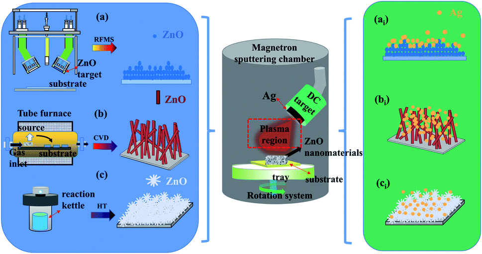 | ||
| Fig. 1 Illustration of preparation process for two-step experiments strategy. The two-step MS (a, ai), two-step CVD and MS (b, bi) and two-step HT and MS (c, ci) strategy. | ||
The surface morphology of the AZO nanomaterials was characterized by using field emission scanning electron microscopy (FE-SEM, Hitachi SEM, model Quanta 200F), atomic force microscopy (AFM) and transmission electron microscopy (TEM, FEI Tecnai F20). The crystal structures and elemental contents of the AZO nanomaterials were studied using X-ray diffractometry (XRD, Siemens D5000) and energy dispersive X-ray spectroscopy (EDS, Hitachi SEM, model Quanta 200F), respectively. The surface atomic composition of O, Zn and Ag were measured using X-ray photoemission spectrometry (XPS, PHI 5700 ESCA System). The optical properties of the AZO nanomaterials were measured using a spectrophotometer (UV-vis, PerkinElmer, and Lambda 850) and room temperature photoluminescence (PL) spectra.35
Results and discussion
Fig. 2a–aiii and b–biii show the SEM and AFM images of the pure ZnO NFm and AZO-150 s NFm, respectively. The surface morphology of both pure ZnO NFm and AZO-150 s NFm are “island-like” and the particle size of ZnO is about 9.8 nm. Fig. 2c shows the SEM image of the pure ZnO NFm after heat treatment at 50 s, 100 °C, and 2 Pa, with a significantly larger particle size of about 16.7 nm compared to that in Fig. 2a. The SEM images of Ag NFm (see Fig. 2d) under sputtering conditions of 100 °C, 50 s, 2 Pa, and 5 W, reveal that the average size of the Ag NPs is about 4.1 nm. The sputtering time of Ag effects the number of Ag NPs deposited (see Fig. 2e), and the variation of the AZO NFm thickness is also effected by the sputtering time of the Ag particles. As shown in the side view SEM image of the AZO NFm (see Fig. 2fi–Ii), the thickness of the AZO NFm increases with the increasing sputtering time of Ag, from 152 to 161 nm. Fig. 2f–I and fii–Iii show front SEM and EDS images of (AZO-50 s NFm), (AZO-100 s NFm), 150 s (AZO-150 s NFm) and (AZO-200 s NFm), respectively. The EDS results demonstrate the ratio of the Ag, O and Zn atomic contents. With this increase in the Ag sputtering time, the number of Ag particles deposited increases. However, the relative content of Ag atoms first increases and then decreases, the relative content of the Zn atoms first decreases, then increases and then decreases, and the relative content of the O atoms first increases, then decreases and finally increases. To explain the above phenomenon, we speculate that (i): as the deposition time of the Ag particles increases, Ag is slightly oxidized, resulting in an increase in the phase content of the Ag atoms with O atoms and a decrease in the relative proportion of Zn atoms. However, the thickness of Ag oxidation is low and the relative content of O atoms cannot increase continuously. (ii): When depositing Ag particles on ZnO NFm, it is equivalent to the secondary heat treatment of ZnO NFm, which will cause O atoms to overflow while enhancing the crystallinity of ZnO NFm. (iii): Owing to the principle of preferential back-sputtering, the Ar in the sputtering chamber strike the ZnO NFm during the sputtering of Ag particles, which may reverse the sputtering of Zn atoms and O atoms, thus effecting the relative contents of Ag, O and Zn atoms. In summary, the sputtering time of Ag particles must be carefully controlled in order to obtain the optimum atomic content of the AZO NFm. | ||
| Fig. 2 SEM and AFM patterns of the unmodified ZnO (a–aiii) and AZO-150 s NFm (b–biii), respectively. SEM patterns of the unmodified ZnO (c) and Ag-50 s NFm (d). (e) The growth process of the AZO NWs with sputtering times of 50, 100, 150 and 200 s. SEM (fi–Ii), side SEM (fi–Ii) and EDS (fii–Iii) images for the unmodified ZnO and AZO NFm with sputtering times of 50, 100, 150 and 200 s, respectively. | ||
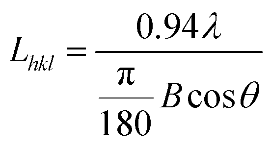
Fig. 3b shows the XRD spectra of the AZO-time NFm and ZnO NFm, two distinct diffraction peaks for (002) (2θ = 34.21°) and (110) (2θ = 56.31°) appear for the pure ZnO NFm, which prove that ZnO NFm has a preferential growth orientation in the (002) and (110) directions. The diffraction peak of the AZO NFm is shifted to the right with respect to pure ZnO NFm, and the angle of the shift increases with the increasing sputtering time of the Ag particles. The reason for this may be: (i) the small amount of Ag doping into ZnO, which distorts the lattice to shift the diffraction peaks of pure ZnO.35 (ii) The small shift in the ZnO NFm diffraction peak is a result of the interfacial stress caused by the contact between the Ag and ZnO.33 Meanwhile, Ag suppresses the diffraction intensity of ZnO in the (100) and (002) directions, and the diffraction peaks in the (002) direction of AZO-100 s NFm and AZO-200 s NFm completely disappeared. In addition, the presence of diffraction peaks, such as Ag2O3 and Ag3O4, prove that a small amount of Ag is not present in the monomer form and is incorporated into the ZnO lattice, which verifies our hypothesis about the diffraction angle shift. The XRD spectra (see Fig. 3b) and the results presented in Table 1 show that the modification of Ag reduces the half-peak width (FWHM) of the ZnO peak (002), and the FWHM values are shown in Table 1. A similar situation has been reported previously, Asmar et al. found that after annealing, the FWHM of the ZnO (002) peak became smaller and the crystal quality of the ZnO film was improved. Kumar et al.14 also found that the FWHM of ZnO (002) became smaller after annealing an AZO NFm grown using MS. According to the Scherrer formula:
 | (1) |
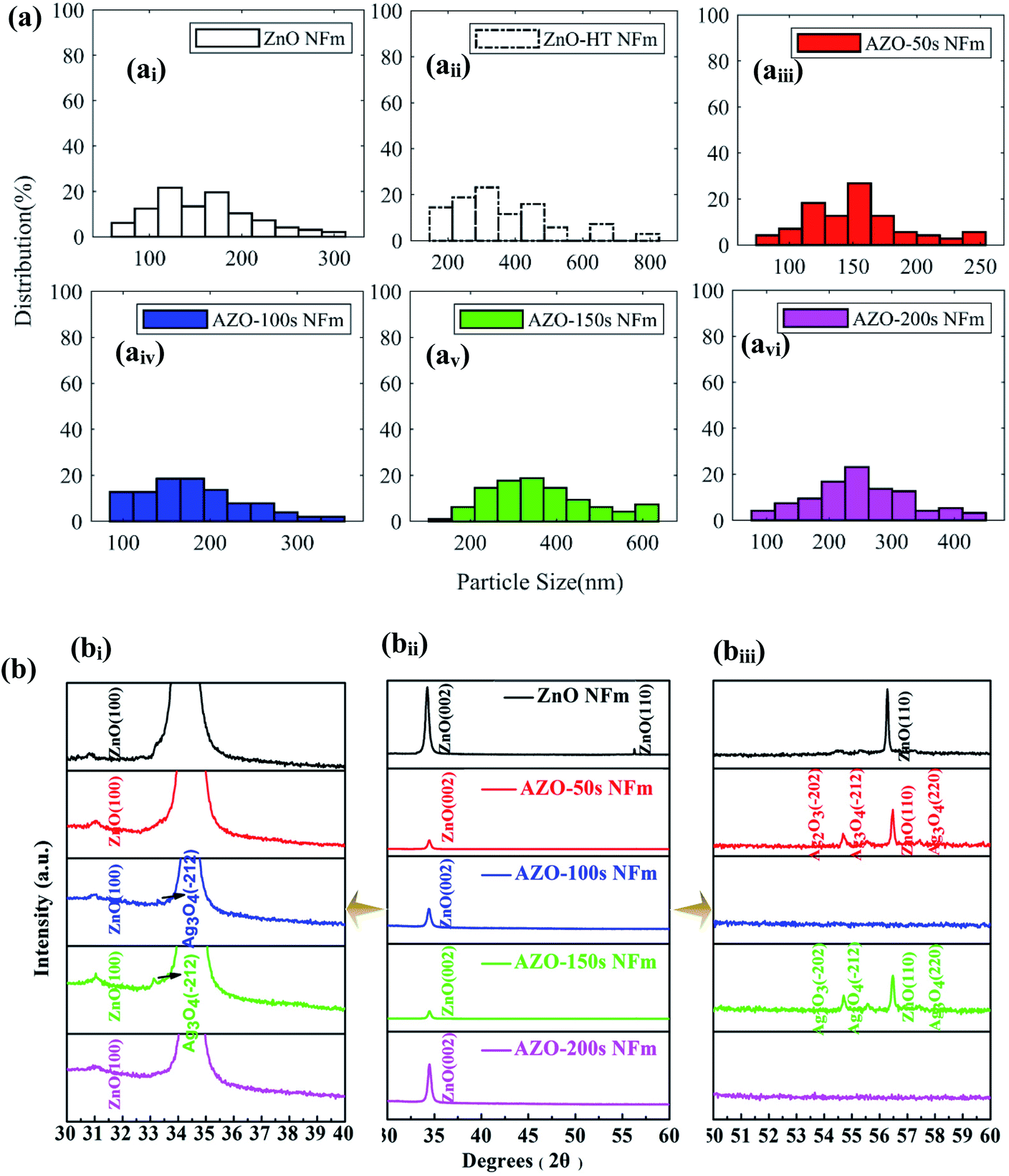 | ||
| Fig. 3 Particle size distribution (ai–avi) and XRD (bi–biii) patterns of pure ZnO and AZO NFm with different sputtering time. | ||
| Parameter | ZnONFm | AZO-50 s NFm | AZO-100 s NFm | AZO-150 s NFm | AZO-200 s NFm |
|---|---|---|---|---|---|
| a/nm | 3.25 | 5.85 | 5.83 | 5.85 | 5.88 |
| b/nm | 3.25 | 3.48 | 3.47 | 3.48 | 3.48 |
| c/nm | 5.21 | 5.49 | 5.48 | 5.50 | 5.49 |
| d/nm | 2.617 | 2.611 | 2.614 | 2.610 | 2.599 |
| D/nm | 14.98 | 16.04 | 19.59 | 38.70 | 27.79 |
| θ/° | 34.242 | 34.319 | 34.280 | 34.334 | 34.482 |
| FWHM/nm | 0.45 | 0.35 | 0.46 | 0.40 | 0.39 |
| Crystallinity | 59.98 | 93.93 | 85.51 | 45.61 | 61.39 |
| Standard deviation | 52.63 | 27.44 | 37.11 | 115.92 | 53.91 |
Fig. 4 shows the SEM, EDS, XRD, TEM, and selected area electron diffraction (SAED) images of the AZO NWs prepared using CVD composite MS. The sputtering times of Ag were maintained at 0 s (unmodified ZnO NWs35), 80 s (AZO-80 s NWs35), 100 s (AZO-100 s NWs35), 150 s (AZO-150 s NWs35), 200 s (AZO-200 s NWs35). The growth process of the AZO NWs is shown in Fig. 4ai–av. In Fig. 4b–f, the SEM and TEM results show that the Ag NPs were adsorbed on ZnO NWs in the form of monomers. The Ag particles with a hemispherical shape were uniformly distributed on ZnO NWs, with the increase in the sputtering time (0–200 s), the density and size of the Ag NPs increased, but when the sputtering time increased to a certain value (150 s), the Ag NPs started to nucleate themselves and agglomeration occurred. In Fig. 4h, the EDS results show that with the increase of Ag sputtering time, the atom relative content of Ag increases, the atom content of Zn decreases, and the atom content of O increases. Theoretically, the atomic ratio of Zn to O in the ZnO materials should be 1![[thin space (1/6-em)]](https://www.rsc.org/images/entities/char_2009.gif) :1. However, owing to the intrinsic donor defects of ZnO, namely the oxygen vacancy (VO) and zinc interstitial (IZn), there is a gap between the atomic ratio of Zn to O in most ZnO materials and the theoretical value. As the sputtering time of the Ag particles increases, the atomic ratio of Zn to O in AZO NWs and AZO NFm gradually adjusts from greater than 2:1 to approximately 1:1, indicating that based on the recombination of Ag NPs the intrinsic defects of ZnO have been modified. The XRD spectra of the AZO NWs are shown in Fig. 4g. The Ag NPs have a (200) peak at the position 2θ = 44.5° (JCPDS no. 04 0783), and the peak intensity of (200) increases with the increase in the Ag sputtering time. The characteristic diffraction peaks of ZnO are (100), (002), (101), (102), (110) and (103), indicating that ZnO has a hexagonal wurtzite structure (JCPDS card no. 76-704), and the diffraction peak for the AZO NWs shows almost no deviation compared with pure ZnO.
:1. However, owing to the intrinsic donor defects of ZnO, namely the oxygen vacancy (VO) and zinc interstitial (IZn), there is a gap between the atomic ratio of Zn to O in most ZnO materials and the theoretical value. As the sputtering time of the Ag particles increases, the atomic ratio of Zn to O in AZO NWs and AZO NFm gradually adjusts from greater than 2:1 to approximately 1:1, indicating that based on the recombination of Ag NPs the intrinsic defects of ZnO have been modified. The XRD spectra of the AZO NWs are shown in Fig. 4g. The Ag NPs have a (200) peak at the position 2θ = 44.5° (JCPDS no. 04 0783), and the peak intensity of (200) increases with the increase in the Ag sputtering time. The characteristic diffraction peaks of ZnO are (100), (002), (101), (102), (110) and (103), indicating that ZnO has a hexagonal wurtzite structure (JCPDS card no. 76-704), and the diffraction peak for the AZO NWs shows almost no deviation compared with pure ZnO.
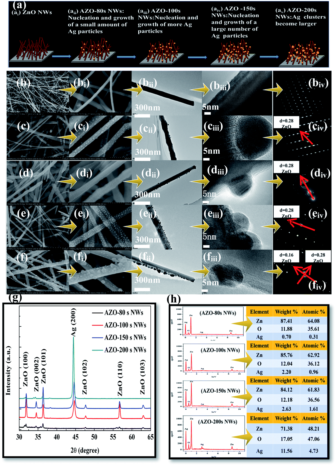 | ||
| Fig. 4 (ai–av) The growth process of AZO NWs with different sputtering time. Low-resolution SEM (b–f) and high-resolution SEM (bi–fi), Low-resolution TEM (bii–fii) and high-resolution TEM (biii–fiii), SAED (biv–fiv), XRD (g) spectra and EDX images (h) for unmodified ZnO and AZO NWs with sputtering time at 80 s, 100 s, 150 s and 200 s, respectively. | ||
The growth process for the AZO-time NFw is shown in Fig. 5a, and the FE-SEM morphologies of the pure ZnO NFw and AZO-time NFw are shown in Fig. 5b–biii and c–f, respectively. The sputtering times of the Ag NPs were kept at 0 s (ZnO NFw), 50 s (AZO-50 s NFw), 100 s (AZO 100 s NFw), 150 s (AZO-150 s NFw), and 200 s (AZO-200 s NFw). From the high resolution transmission electron microscopy (HRTEM) of Fig. 5cii–fi, it can be seen that the average diameter of the Ag NPs is a few nanometers and ellipsoidal Ag NPs are uniformly attached to the surface of ZnO NFw in the form of monomers. The SAED plots (see Fig. 5cii–fii) show that both the AZO NFw and ZnO NFw are polycrystalline and have a high crystalline quality, and the compounding of the Ag NPs did not change the structure of ZnO NFw. As the Ag NPs are adsorbed on the nucleus edge of the ZnO NFw by reducing the interfacial energy of ZnO NFw, the Ag NPs are not uniformly distributed on the surface of the AZO NFw. The distribution of EDS elements indicates the presence of AZO NFw, and significant Ag, Zn and O peaks are observed in the AZO NFw as shown in Fig. 5h. As the sputtering time for the Ag particles increases, the relative content of the Ag and Zn atoms increases, and the relative content of the O atoms decreases. The increase in the ratio of the relative atomic content of Zn to O means the increased number of intrinsic sender defects in AZO NFw will capture more electrons and thus prolong the photogenerated electron–hole lifetime. As shown in Fig. 5g, the XRD diffraction peaks of the AZO-time NFw are shifted relative to the pure ZnO NFw, which originate from the interfacial stress at Ag between ZnO. Analysis of the XRD results of the AZO-time NFw has been fully demonstrated in previous work from this group,40 and is not described in detail here.
 | ||
| Fig. 5 (ai–aiv) The growth process of AZO NFw with the different sputtering time. SEM (b–biii) of unmodified ZnO NFw. SEM (c–f), HRTEM (ci–fi), SAED (cii–fii) patterns of AZO NFw with the different sputtering time at 50 s, 100 s, 150 s and 200 s, respectively. The XRD (g) spectra and EDX spectra (h) for the samples, respectively. | ||
Diffraction peaks of the singlet Ag elements were not observed in the AZO NFm, and we could not identify the exact state of the Ag elements. Therefore, we performed XPS analysis of AZO-150 s NFm. In Fig. 6b, the peaks at 1024.6 and 1047.6 eV correspond to the electronic states of Zn3/2 and Zn1/2, respectively, corresponding to the binding energy of Zn2+ in ZnO.41 Owing to the presence of AgxOy in the sample, the increase of VO on the ZnO surface leads to a shift of the Zn3/2 and Zn1/2 peaks to higher positions, with a valence difference between the two peaks of about 23 eV. In Fig. 6d, the peaks at 370.3 and 376.3 eV correspond to the electronic states of Ag5/2 and Ag3/2, respectively. The energy difference (6.0 eV) between the two Ag peaks indicates the presence of Ag in the positive valence state, as well as in the singlet form. Compared to the standard electronic binding energy of Ag (368.2 eV, 374.2 eV),50 among our AZO NFm preparations, Ag showed a higher binding energy. This is related to the interaction of Ag with ZnO. This shift in binding energy can be explained by the energy band theory;42 if Ag and ZnO are in contact, the transfer of electrons occurs from the Ag surface to the ZnO surface and results in a new Fermi energy level equilibrium owing to the different work functions of the two materials at the contact surface, causing the electron deficiency of Ag,42 which results in a shift in the binding energy of Ag.50 This partially generates monovalent Ag in AZO NFm, which possesses a lower binding energy of Ag 3d 5/2 as compared with Ag0. The XPS results confirmed the successful preparation of AZO NFm, with some Ag adsorbed on the ZnO surface in the form of a singlet. The rest of the Ag doped into the ZnO lattice verifies our above speculation.
 | ||
| Fig. 6 XPS spectra of AZO-150 s NFm (a) (Zn 2p (b), O 1s (c) and Ag 3d (d)). | ||
The growth mechanism of the AZO NFm is shown schematically in Fig. 7a. The growth of pure ZnO NFm shows a distinct island growth, Fig. 7ai–aiii shows a very obvious columnar growth feature, and the top of the column is very flat. ZnO NFm has a layer-by-layer growth at the top of the island. According to the crystal nucleation theory,39 the growth mechanism belongs to the layered solidification model because the bonding between the generated atoms is weaker than the bonding between the substrates, that is, the desorption energy (K1) is larger than the sublimation energy (K2). In Fig. 7aiv–avi, the Ag NPs do not easily replace the Zn position when Ag is under the lower deposition temperature, and the Ag NPs more easily adsorb onto the ZnO NFm surface. When the desorption energy of ZnO for Ag is larger than the sublimation energy of Ag, and there is an uneven protrusion of ZnO NFm in addition to the Volmer–Weber type of growth of Ag, the island growth of Ag is promoted. When the Ag particles completely cover the ZnO NFm surface, the film surface will still become partially bumpy. At the same time, when the desorption energy of Ag to itself is less than the sublimation energy, this leads to the nucleation and growth of Ag by itself. The above described results theoretically confirm our previous conjecture about the growth mechanism of the thin film.
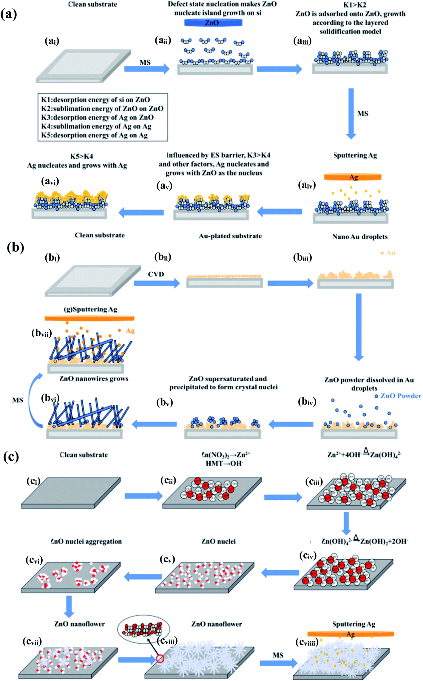 | ||
| Fig. 7 Growth mechanism of the AZO nanomaterials (including NFm (ai–aiv), NWs (bi–biv) and NFw (ci–cviiii)) | ||
The growth mechanism of the ZnO NWs can be explained by the gas–liquid–solid (VLS) mechanism.43–45 The growth mechanism diagram of ZnO NWs is shown in Fig. 7b, this shows that the vacuum heat treatment causes the formation of gold nanodroplets on the gold-plated substrate, and the ZnO powder is adsorbed and dissolved in the droplets after vacuum heat treatment (see Fig. 7bii). If the dissolution limit is reached, the supersaturated ZnO precipitates from the droplet surface and forms nuclei (Fig. 7biii), which eventually form a one-dimensional structure, for example, ZnO NWs (Fig. 7biv–bvi). Gold plays a catalytic role here and the gold droplets also guide the growth of ZnO NWs on the substrate. Therefore, what finally appears is the tilted growth of the ZnO NWs (see Fig. 7bvi). As the desorption energy of the Ag on ZnO is greater than the sublimation energy of Ag, Ag NPs are hemispherically and uniformly adsorbed on the ZnO NWs (Fig. 7bvii). The biggest difference between ZnO NWs and ZnO NFm is that the surface of the ZnO NWs is relatively smooth, therefore the morphology of the Ag growing on the surface of the ZnO NWs is not affected by the surface inhomogeneity. This leads to the existence of Ag, mainly in the form of solid Ag, which is smaller than the critical nucleus size. As a result, the morphology of Ag forms a spherical core, showing a very typical hemispherical shape. Under the same Ar flux and vacuum conditions, Ag does not readily form oxides, which is clearly related to the Ag growth environment. Comparison of the XRD peak sharpness indicates that the crystallinity of AZO NWs is better than that of the AZO NFm. One reason is that the AZO NWs grow at a high temperature and there is no recrystallization process after compounding with Ag. Meanwhile, the higher temperature in the preparation of AZO NWs is favorable for the synthesis of high crystallinity composites; on the other hand, the presence of gold droplets during the growth of AZO NWs promotes the growth of AZO NWs in one direction and enhances its crystallinity. The growth mechanisms of ZnO NFw and AZO NFw are shown in Fig. 7c. During the growth of the ZnO NFw, hexamethyltetramine (HMT) provides OH− and Zn(NO3)2 provides Zn2+ (Fig. 7cii). OH− combines with Zn2+ to form Zn(OH)2− (see Fig. 7ciii), and Zn(OH)2− is decomposed and oxidized by heating to form ZnO nuclei that gradually form the flower-like structure of ZnO NFw. Subsequently, Ag particles are deposited on the surface of the ZnO NFw by MS to form AZO NFw (Fig. 7cviii).
In summary, no matter which preparation method is used for the fabrication of the ZnO nanostructures, CVD or MS, different growth methods lead to very different morphologies, growth processes, and crystals of ZnO samples. Although their growth mechanisms are different, they all have a common strong nucleation growth, which is undoubtedly related to factors such as the preferential growth mechanism of particles, defect nucleation, lattice-mismatch induced-stress, and so forth. These factors make ZnO grow in a more optimal direction while restricting the growth in other directions. This is the reason why one dimensional (1D) ZnO nanostructures are mostly linear and rod-like, while 2D ZnO nanostructures, such as ZnO NFm, are mostly island-like when grown, and 3D ZnO nanostructures are flower-like.
The optical properties of the ZnO and AZO nanomaterials alone are the key factors affecting their applications. Fig. 8a shows the UV-vis absorption spectra of AZO NFm. The peak at 367 nm belongs to the quadrupole resonance excitation of the Ag NPs, and the surface plasmon band of the AZO NFm composite is significantly wider and red-shifted compared to the pure Ag nanowires, which may be due to the strong interfacial electronic coupling between the ZnO and Ag NPs.47 The order of the near-UV-visible absorption peak intensity of the AZO NFm is: ZnO NFm < AZO-200 s NFm < AZO-150 s NFm < AZO-100 s NFm < AZO-50 s NFm. The absorption intensity of the AZO NFm is greater than that of the ZnO NFm. With the increase in the sputtering time of the Ag particles, the absorption intensity of the AZO NFm decreases instead. Fig. 8b and c shows the UV-vis absorption spectra of the AZO NWs, AZO NFw, ZnO NWs and AZO NFw, respectively. The intensity of the absorption peaks of the AZO NWs and AZO NFw decreases and then increases with the increase in the Ag sputtering time. The reasons for the above phenomenon may be (i) the peak at 380 nm corresponds to the transverse plasmon resonance of Ag,47 and the intrinsic absorption peak of pure ZnO is located at 378 nm, forming a double excited state when ZnO and Ag are excited by the same photon,51 thus the photon can be absorbed, intensified, and diverted to ZnO by the Ag NPs to perform further absorption. (ii) As the work of the Ag function is larger than that of ZnO, there is charge transfer if Ag is in contact with ZnO, and the electron loss on the Ag surface weakens the ZnO absorption, and the Schottky contact (SB)51 between Ag and ZnO facilitates ZnO electron–hole separation, which enhances the ZnO photon absorption. (iii) The number of Ag NPs increases with the increase in the Ag particle sputtering time, and when the ZnO surface is covered by metallic Ag the enhancement of the mirror effect of Ag makes the light absorption performance of ZnO weaker.
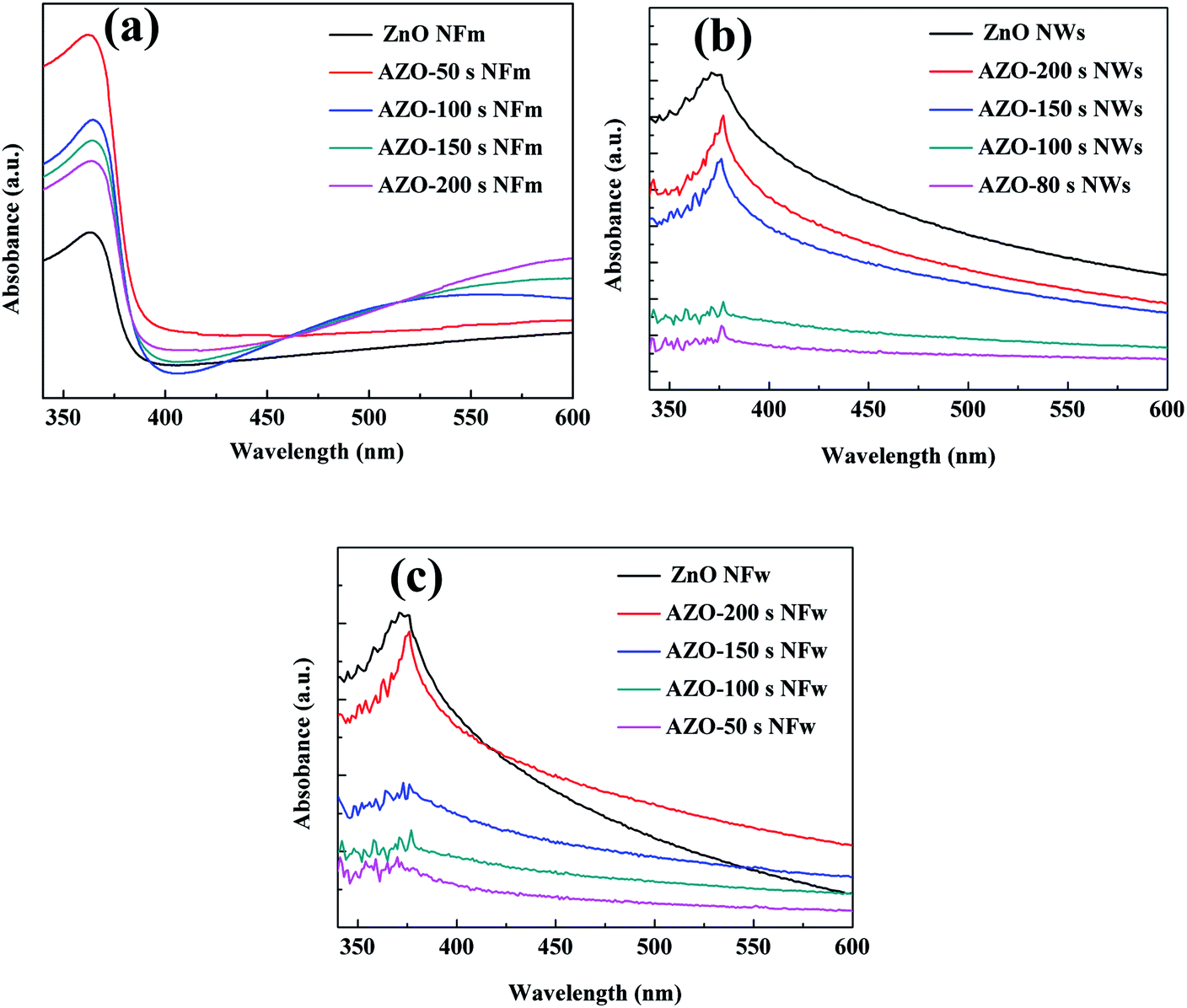 | ||
| Fig. 8 UV-vis absorption spectra of the unmodified ZnO and AZO NFm (a), NWs (b) and NFs (c) with different sputtering times. | ||
From the results of the UV-vis experiments, it can be seen that the morphology of ZnO affects the position and intensity of the AZO absorption peaks. The AZO NFm prepared using the two-step MS method has excellent photo absorption properties, while the highest absorption peak intensity is observed for the AZO-50 s NFm. In Fig. 8a–c, different dimensions (1–3D) of ZnO were found to affect its optical absorption edge and energy band gap. The band gap values of the AZO composites are all smaller than those of ZnO as determined by the position of the absorption edge of AZO, which is due to the increase in defects and impurities in AZO.
The results of room temperature PL experiments for ZnO NFm and AZO NFm are shown in Fig. 9a–aii, both of which have significant emission peaks at 385, 590, 630, and 770 nm. The UV emission (385 nm) corresponds to the near-band edge emission (NBE),43,44 which originates from the free exciton radiation complex. Compared to ZnO NFm, the AZO NFm UV emission, as well as the intensity of the yellow-green and red-light emission located at 630 and 770 nm, respectively, are significantly changed. In Fig. 9ai, the order of variation of the UV emission peak intensity for sputtering times (50–200 s) is: ZnO NFm > AZO-50 s NFm > AZO-100 s NFm > AZO-200 s NFm > AZO-150 s NFm. The yellow-green and red-light emissions are caused by VO or IZn gap defects electron–hole complex (DL)43,44 (see Fig. 9aii), the yellow-green and red luminescence intensities vary in the following order: ZnO NFm > AZO-100 s NFm > AZO-200 s NFm > AZO-50 s NFm > AZO-150 s NFm. The reasons for the change in the PL intensity of ZnO are as follows: firstly the adsorption of Ag changes the defect state and the number of exciton pairs on the surface of ZnO,48 the abundant surface state is favorable for the PL signal of ZnO. Secondly the exciton of ZnO coupled with the surface plasmon resonance of the Ag NPs results in a change in the local field. The large size mismatch between the optical wavelength and the ZnO excitons leads to weak light–matter interactions, which hinder efficient energy conversion. In contrast, the plasma of Ag as a collective oscillation mode of electrons can break the diffraction limit and strongly couple with the external field to obtain a large near-field enhancement. This enhanced local field can interact strongly with the neighboring ZnO exciton pairs, and the excitons appearing in the plasma near field can in turn change the optical properties of the plasma.52 Finally, ZnO and Ag form semiconductor–metal junctions, and the over doping of Ag forms AgxOy, and so forth, producing a strong non-radiative complex Auger process.22,49 The Auger process will rapidly deplete the electron–hole pairs, reducing the PL intensity.
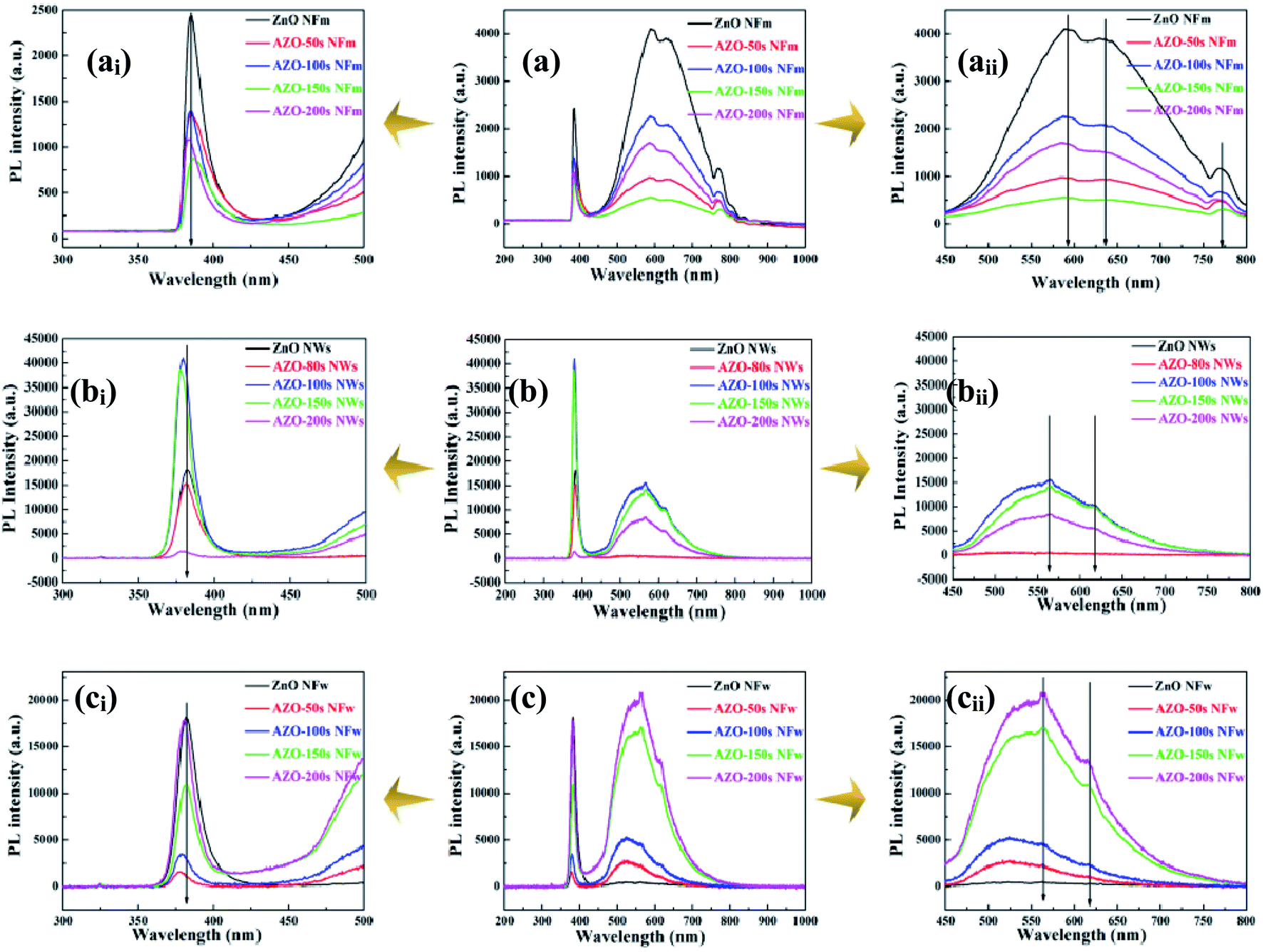 | ||
| Fig. 9 The PL spectra of the unmodified ZnO and AZO (NFm (a–aii), NWs (b–bii) and NFw (c–cii)) with different sputtering times. | ||
For yellow, green and red emission peaks, pure ZnO NFm is stronger than the ZnO NWs (see Fig. 9a and b), but the UV emission intensity of ZnO NFm is reduced and the yellow-green emission intensity of the ZnO NWs is smaller than that of ZnO NFm. The Ag composite decreases the NEB and DL emissions of the ZnO NWs, which are different from those of the ZnO NFm composite Ag. This is not only a result of the decrease in the PL strength caused by the SB and Auger process between Ag and ZnO, but also the growth mechanism of ZnO. As the crystallinity of ZnO NWs is stronger than that of ZnO NFm, there are fewer defects and fewer captured electrons, therefore the UV emission intensity of the ZnO NWs is higher and the emission in the visible region is lower. Fig. 9c shows the PL diagram of the pure ZnO NFw and AZO NFw. Under the excitation laser with a wavelength of 325 nm, Fig. 9ci and cii, respectively, shows obvious luminescence characteristics in the UV and visible regions. It can be seen from Fig. 9ci that the UV emission peak is located at 387 nm, which is caused by the recombination of the free excitons. In Fig. 9cii, the central wavelengths of the green and yellow emissions are located at 530 and 594 nm, respectively. Owing to the defects in VO and IZn,46 the visible emission band is considered to be close to the defect luminescence. The green luminescence of AZO NFw comes from the VO and surface states, or the combination of holes and electronic states of a specific defect.46 It can be seen from Fig. 9ci and cii that the luminous peak intensity of AZO NFw in the visible region is higher than that of pure ZnO NFw, this is mainly the result of the interaction between the SPR of the Ag NPs and the incident electromagnetic field of the 325 nm laser. The above experimental results show that local field enhancement close to the Ag NPs can improve the electron excitation rate of the ZnO.46 When the electron excitation rate is greater than the electron–hole recombination rate, the PL emission peak of AZO is stronger than that of ZnO. When the electron excitation rate is less than the electron–hole recombination rate, the result is reversed. Moreover, AZO composites with different growth mechanisms have different luminescence characteristics. The plasma nature of the Ag NPs leads to a more efficient conversion of the captured electrons into excited light, suggesting that plasma-coupled luminescence can be used to improve the development of radiation detectors.
Conclusion
In summary, we studied the growth mechanism, crystal structure and optical characteristics of AZO NFm, AZO NWs and AZO NFw. The results show that the Ag NPs grow on the surface of ZnO NFm, first with ZnO as the core and then self-nucleated, which is undoubtedly affected by the island growth of ZnO NFm and the ES barrier factor. When Ag grows on ZnO NWs and ZnO NFw, Ag is more likely to self-nucleate owing to the roughness of the ZnO NWs and ZnO NFw. The SEM and TEM results show that the content and distribution of Ag can be controlled by adjusting the sputtering time of Ag. The XRD results show that Ag is more likely to combine with oxygen in ZnO NFm prepared by MS owing to the influence of the growth mechanism, resulting in AgxOy and the slightly lower crystallinity of AZO NFm. However, when Ag is compounded on the ZnO NWs and ZnO NFw, they mostly exist in the form of Ag monomers with a good crystallinity. The absorption peak intensity of AZO NFm changes with the increase in the Ag sputtering time, and AZO-50 s NFm has the strongest absorption peak in the UV region. The UV results of the AZO NWs and AZO NFw show that the deposition of Ag particles decreases the absorption intensity of ZnO in the full wave range. In addition, the PL results of AZO nanomaterials showed that the emission peak of AZO NFm was weaker than that of the pure ZnO nanomaterials, and the PL peak of the AZO NWs and AZO NFw was stronger than that of the pure ZnO nanomaterials. The results show that AZO nanomaterials with different morphologies can be used in different optical applications. AZO materials have great potential for applications in flat panel displays, high brightness electron sources, field emission devices and solar cells.Conflicts of interest
There are no conflicts to declare.Acknowledgements
This work was supported by the Natural Science Foundation of Heilongjiang Province under Grant No. LH2021A016, and Harbin Normal University under Grant No. 2020-KYYWF352 and HSDSSCX2021-28.References
- D. P. Norton, Y. Heo, M. Ivill, K. Ip, S. Pearton, M. F. Chisholm and T. Steiner, ZnO: growth, doping & processing, Mater. Today, 2004, 7, 34–40 CrossRef CAS.
- J. Chang, H. Kuo, I. Leu and M. Hon, The effects of thickness and operation temperature on ZnO: Al thin film CO gas sensor, Sens. Actuators, B, 2002, 84, 258–264 CrossRef CAS.
- G. Lashkarev, I. Shtepliuk, A. Ievtushenko, O. Khyzhun, V. Kartuzov, L. Ovsiannikova, V. Karpyna, D. Myroniuk, V. Khomyak and V. Tkach, Properties of solid solutions, doped film, and nanocomposite structures based on zinc oxide, Low Temp. Phys., 2015, 41, 129–140 CrossRef CAS.
- X. Tan, S. Zhou, H. J. Tao, W. Y. Wang, Q. W. Wan and K. C. Zhang, Influence of Ag on photocatalytic performance of Ag/ZnO nanosheet photocatalysts, J. Cent. South Univ., 2019, 26, 2011–2018 CrossRef CAS.
- E. Skiba, S. Michlewska, M. Pietrzak and W. M. Wolf, Additive interactions of nanoparticulate ZnO with copper, manganese and iron in Pisum sativum L., a hydroponic study, Sci. Rep., 2020, 10, 1–10 CrossRef PubMed.
- I. S. Kim, E.-K. Jeong, D. Y. Kim, M. Kumar and S.-Y. Choi, Investigation of p-type behavior in Ag-doped ZnO thin films by E-beam evaporation, Appl. Surf. Sci., 2009, 255, 4011–4014 CrossRef CAS.
- W. Li, C. Kong, H. Ruan, G. Qin, G. Huang, T. Yang, W. Liang, Y. Zhao, X. Meng and P. Yu, Electrical properties and Raman scattering investigation of Ag doped ZnO thin films, Solid State Commun., 2012, 152, 147–150 CrossRef CAS.
- Q. Diao, Y. Yin, X. Zhang, J. Li, M. Jiao, J. Cao, Q. Qin, K. Yang, G. Zhu and X. Xu, Fabrication of ZnO@ CeO2 core–shell hetero-structural nanofibers and enhanced gas sensing performance for acetone, Funct. Mater. Lett., 2020, 13, 2050013 CrossRef CAS.
- M. Shkir, B. M. Al-Shehri, M. Pachamuthu, A. Khan, K. V. Chandekar, S. AlFaify and M. S. Hamdy, A remarkable improvement in photocatalytic activity of ZnO nanoparticles through Sr doping synthesized by one pot flash combustion technique for water treatments, Colloids Surf., A, 2020, 587, 124340 CrossRef CAS.
- R. Peña-Garcia, Y. Guerra, R. Milani, D. Oliveira, F. de Souza and E. Padrón-Hernández, Influence of Ni and Sr on the structural, morphological and optical properties of ZnO synthesized by sol gel, Opt. Mater., 2019, 98, 109427 CrossRef.
- P. Raghavendra, J. Bhat and N. Deshpande, Enhancement of photoluminescence in Sr doped ZnO thin films prepared by spray pyrolysis, Mater. Sci. Semicond. Process., 2017, 68, 262–269 CrossRef CAS.
- S. Narasimman, L. Balakrishnan and Z. Alex, Clad-modified fiber optic ammonia sensor based on Cu functionalized ZnO nanoflakes, Sens. Actuators, A, 2020, 316, 112374 CrossRef CAS.
- Y. Han, C. B. Yao, Y. Cai, S. B. Bao and G. Q. Jiang, Copper decorated ZnO nanowires material: Growth, optical and photoelectrochemical properties, J. Alloys Compd., 2020, 835, 155339 CrossRef CAS.
- V. S. Kumar and D. Kanjilal, Influence of post-deposition annealing on structural, optical and transport properties of nanocomposite ZnO-Ag thin films, Mater. Sci. Semicond. Process., 2018, 81, 22–29 CrossRef CAS.
- J. C. Bian, F. Yang, Z. Li, J. L. Zeng, X. W. Zhang, Z. D. Chen, J. Z. Y. Tan, R. Q. Peng, H. Y. He and J. Wang, Mechanisms in photoluminescence enhancement of ZnO nanorod arrays by the localized surface plasmons of Ag nanoparticles, Appl. Surf. Sci., 2012, 258, 8548–8551 CrossRef CAS.
- K. Ozga, T. Kawaharamura, A. A. Umar, M. Oyama, K. Nouneh, A. Slezak, S. Fujita, M. Piasecki, A. Reshak and I. Kityk, Second order optical effects in Au nanoparticle-deposited ZnO nanocrystallite films, Nanotechnology, 2008, 19, 185709 CrossRef CAS PubMed.
- C. L. Hsu, L. F. Chang and T. J. Hsueh, A dual-band photodetector based on ZnO nanowires decorated with Au nanoparticles synthesized on a glass substrate, RSC Adv., 2016, 6, 74201–74208 RSC.
- N. Q. Yang, J. Li, Y. N. Wang and J. Ma, Investigation of photocatalytic properties based on Fe and Ce Co-doped ZnO via hydrothermal method and first principles, Mater. Sci. Semicond. Process., 2021, 131, 105835 CrossRef CAS.
- Z. W. Chen, C. B. Yao, Y. Han, S. B. Bao, G. Q. Jiang and Y. Cai, Synthesis, structure and femtosecond nonlinear absorption properties of Ce-ZnO films, Appl. Surf. Sci., 2020, 502, 144133 CrossRef CAS.
- J. Fan and R. Freer, The roles played by Ag and Al dopants in controlling the electrical properties of ZnO varistors, J. Appl. Phys., 1995, 77, 4795–4800 CrossRef CAS.
- M. Thomas and J. Cui, Investigations of acceptor related photoluminescence from electrodeposited Ag-doped ZnO, J. Appl. Phys., 2009, 105, 093533 CrossRef.
- A. Ievtushenko, V. Karpyna, J. Eriksson, I. Tsiaoussis, I. Shtepliuk, G. Lashkarev, R. Yakimova and V. Khranovskyy, Effect of Ag doping on the structural, electrical and optical properties of ZnO grown by MOCVD at different substrate temperatures, Superlattices Microstruct., 2018, 117, 121–131 CrossRef CAS.
- J. Wang and A. Ning, Enhanced efficient and sensitive SERS sensing via controlled Ag-nanoparticle-decorated 3D flower-like ZnO hierarchical microstructure, Micro Nano Lett., 2020, 15, 1126–1129 CrossRef.
- O. Długosz and M. Banach, Continuous synthesis of photocatalytic nanoparticles of pure ZnO and ZnO modified with metal nanoparticles, J. Nanostruct. Chem., 2021, 1–17 Search PubMed.
- F. Shan, G. Liu, W. Lee, K. Bae, B. Shin and H. Kim, Structural, electrical, and optical properties of Na-doped ZnO thin films deposited by pulsed laser deposition, J. Nanosci. Nanotechnol., 2008, 8, 5203–5207 CrossRef CAS PubMed.
- Z. W. Chen, C. B. Yao and J. Y. Hu, The nonlinear optical properties and optical transition dynamics of Er doped ZnO films, Opt. Laser Technol., 2019, 119, 105609 CrossRef.
- M. Zirak, H. Alehdaghi and A. M. Shakoori, Preparation of ZnO-carbon quantum dot composite thin films with superhydrophilic surface, Mater. Technol., 2021, 36, 72–80 CrossRef CAS.
- M. Iftekhar Uddin, D. T. Phan and G. S. Chung, Low temperature acetylene gas sensor based on Ag nanoparticles-loaded ZnO-reduced graphene oxide hybrid, Sens. Actuators, B, 2015, 207, 362–369 CrossRef.
- C. Yang, Y. K. Su, M. Y. Chuang, H. C. Yu and C. H. Hsiao, Enhanced Field Emission Properties of Ag Nanoparticle-Decorated ZnO Nanorods Under Ultraviolet Illumination, IEEE Trans. Electron Devices, 2015, 62, 2300–2305 CAS.
- Y. H. Ko and J. S. Yu, Silver nanoparticle decorated ZnO nanorod arrays on AZO films for light absorption enhancement, Phys. Status Solidi A, 2012, 209, 297–301 CrossRef CAS.
- P. Zuo, L. Jiang, X. Li, B. Li, P. Ran, X. J. Li, L. T. Qu and Y. F. Lu, Metal (Ag, Pt) MoS2 Hybrids Greenly Prepared Through Photochemical Reduction of Femtosecond Laser Pulses for SERS and HER, ACS Sustainable Chem. Eng., 2018, 6, 7704–7714 CrossRef CAS.
- S. K. Mahatha and K. Menon, Quantum well states in Ag thin films on MoS2(0001) surfaces, J. Phys.: Condens. Matter, 2013, 25(8), 115501–115508 CrossRef CAS PubMed.
- X. Sun, R. Hong, H. Hou, X. F. Zheng and D. S. Jian, Thickness dependence of structure and optical properties of silver films deposited by magnetron sputtering, Thin Solid Films, 2007, 515, 6962–6966 CrossRef CAS.
- K. X. Zhang, X. Wen, C. B. Yao, J. Li, M. Zhang, Q. H. Li, W. J. Sun and J. D. Wu, Synthesis, structural and optical properties of silver nanoparticles uniformly decorated ZnO nanowires, Chem. Phys. Lett., 2018, 698, 147–151 CrossRef CAS.
- K. X. Zhang, C. B. Yao, X. Wen, Q. H. Li and W. J. Sun, Ultrafast nonlinear optical properties and carrier dynamics of silver nanoparticle-decorated ZnO nanowires, RSC Adv., 2018, 8, 26133–26143 RSC.
- K. Butcher, P. P.-T. Chen, M. Godlewski, A. Szczerbakow, E. Goldys, T. Tansley and J. Freitas Jr, Recrystallization prospects for freestanding low-temperature GaN grown using ZnO buffer layers, J. Cryst. Growth, 2002, 246, 237–243 CrossRef CAS.
- R. Al Asmar, G. Ferblantier, J. Sauvajol, A. Giani, A. Khoury and A. Foucaran, Fabrication and characterisation of high quality ZnO thin films by reactive electron beam evaporation technique, Microelectron. J., 2005, 36, 694–699 CrossRef CAS.
- A. Ziabicki, Multidimensional theory of crystal nucleation, in Mathematical Modelling for Polymer Processing, Springer, 2003, pp. 59–117 Search PubMed.
- Y. Cai and C. B. Yao, Study of well-aligned Ag@ZnO nanoflower arrays with growth, photoluminescence and ultrafast nonlinearabsorption properties, Opt. Mater., 2021, 120, 111383 CrossRef CAS.
- W. Li, L. Fang, H. Ruan, G. Qin, P. Zhang, H. Zhang, L. Ye and C. Kong, Oxygen vacancies induced ferromagnetism in Ag–N codoped ZnO thin films, Mater. Lett., 2015, 143, 128–130 CrossRef CAS.
- Y. Lai, M. Meng and Y. Yu, One-step synthesis, characterizations and mechanistic study of nanosheets-constructed fluffy ZnO and Ag/ZnO spheres used for Rhodamine B photodegradation, Appl. Catal., B, 2010, 100, 491–501 CrossRef CAS.
- N. S. Ramgir, K. Subannajui, Y. Yang, R. Grimm, R. Michiels and M. Zacharias, Reactive VLS and the reversible switching between VS and VLS growth modes for ZnO nanowire growth, J. Phys. Chem. C, 2010, 114, 10323–10329 CrossRef CAS.
- J. Huang, L. Zhu, L. Hu, S. Liu, J. Zhang, H. Zhang, X. Yang, L. Sun, D. Li and Z. Ye, Island nucleation, optical and ferromagnetic properties of vertically aligned secondary growth ZnO: Cu nanorod arrays, Nanoscale, 2012, 4, 1627–1635 RSC.
- Y. Yang, Y. Feng and G. Yang, Experimental evidence and physical understanding of ZnO vapor-liquid-solid nanowire growth, Appl. Phys. A: Mater. Sci. Process., 2011, 102, 319–323 CrossRef CAS.
- Y. Zhang and J. Mu, One-pot synthesis, photoluminescence, and photocatalysis of Ag/ZnO composites, J. Colloid Interface Sci., 2007, 309, 478–484 CrossRef CAS PubMed.
- G. Zhang, C. Deng, H. Shi, B. Zou, Y. Li, T. Liu and W. Wang, ZnO/Ag composite nanoflowers as substrates for surface-enhanced Raman scattering, Appl. Surf. Sci., 2017, 402, 154–160 CrossRef CAS.
- H. Liu, G. Shao, J. Zhao, Z. Zhang, Y. Zhang, J. Liang, X. Liu, H. Jia and B. Xu, Worm-like Ag/ZnO core–shell heterostructural composites: fabrication, characterization, and photocatalysis, J. Phys. Chem. C, 2012, 116, 16182–16190 CrossRef CAS.
- J. Yang, H. Zhang, X. Wang, L. Miao and Y. Yang, Optical properties of Ag doped ZnO nanocrystals prepared by hydrothermal and photodeposition method, J. Mater. Sci.: Mater. Electron., 2013, 24, 3430–3434 CrossRef CAS.
- C. H. Ahn, Y. Y. Kim and H. K. Cho, Influence of Synthesis Temperature on the Properties of Ga-Doped ZnO Nanorods Grown by Thermal Evaporation, J. Nanosci. Nanotechnol., 2011, 11, 458 CrossRef CAS PubMed.
- L. Zhi, G. Wang, Q. Yang, Z. Shao and Y. Wang, Synthesis and electrical property of metal/ZnO coaxial nanocables, Nanoscale Res. Lett., 2012, 7, 316 CrossRef PubMed.
- X. Zhang, Y. L. Chen, R. S. Liu and D. P. Tsai, Plasmonic photocatalysis, Rep. Prog. Phys., 2013, 76, 046401 CrossRef PubMed.
- X. Li, L. Zhou, Z. Hao and Q. Q. Wang, Plasmon–Exciton Coupling in Complex Systems, Adv. Opt. Mater., 2018, 18, 1800275 CrossRef.
| This journal is © The Royal Society of Chemistry 2022 |