
 Open Access Article
 This Open Access Article is licensed under a Creative Commons Attribution-Non Commercial 3.0 Unported Licence
Fabrication of a thin PDMS film with complex liquid metal electrodes embedded and its application as skin sensors
Zi Yeab,
Qian Liab,
Renchang Zhangab,
Pan Zhangab and
Lin Gui *ab
*ab
aKey Laboratory of Cryogenics, Technical Institute of Physics and Chemistry, Chinese Academy of Sciences, 29 Zhongguancun East Road, Haidian District, Beijing 100190, China. E-mail: lingui@mail.ipc.ac.cn
bSchool of Future Technology, University of Chinese Academy of Sciences, Beijing 100039, China
First published on 16th March 2022
Abstract
This research work reports an approach for the fabrication of liquid metal patterned thin films. By using this method, very complex liquid metal electrodes can be successfully integrated into a thin PDMS film with a thickness as low as 119 μm. The high resolution of the microelectrode channel is achieved by soft lithography technology. The relatively-thin electrode structure is developed with the assistance of the reversible PC membrane bonding technique that we reported earlier. Femtosecond laser drilling is applied in this work to drill small holes at the channel ends, allowing the air to escape during the filling of liquid metal and making the blind-end liquid metal electrode structure possible. In this work, the fabrication process with some key procedures involved is introduced for developing a microelectrode. Further, a wearable strain sensor is designed with the fabricated microelectrode to show its potential to be used in flexible electronics.
Introduction
Electrodes are the most essential components in microfluidic chips, and in many cases, the flexibility of the microelectrode has become a requirement in microfluidics,1 and applications, such as wearable sensing,2 flexible electronics,3 or as part of soft robotics,4 consist of a substrate and channels. Flexible electrodes in microfluidics are either simply used to conduct current or transmit electrical information,5 or on more complicated occasions used as part of flexible sensors and sometimes even as sensing elements themselves.6,7 To conduct electrical signals, these flexible microelectrodes are developed with different designs and structures to fit as the main components in microfluidics chips. Therefore, the resolution and precision of these electrodes should be similar to or even higher than the designed microchannel or microstructures. For those sensors where microelectrodes are directly employed as sensing components or those used in flexible sensors, the sensing environment may require extra functionality of microelectrodes. For example, the electrodes used in the development of strain sensors should be stretchable.The flexibility of material usually gets larger with smaller thickness and therefore, one approach to fabricate flexible microelectrodes is to make electrode material thin enough. Microelectrodes based on the solid form of metal or metallic compounds are usually made flexible through this approach.8–11 The advantages of these microelectrodes are high electrical conductivity, a simple fabrication process, and ultra-thin structures. However, the usual fabrication process of this type of electrode includes screen-printing12 or an approach called ‘cut-and-paste’.9 The resolution of both these two approaches is limited (mm scale12 and 600 μm (ref. 9) resolution, respectively) compared with more detailed fabrication processes like soft lithography and also, because the normally seen resolution in the microfluidic channel is around tens to a few hundred microns, the size of the electrodes is found to be too large to be used in microfluidics. Besides, these metal and metallic compounds are usually not very stretchable. Also, to increase the robustness during stretching, very complicated electrode structures are usually designed which makes the electrode size even larger.8,13 Room-temperature liquid metal, on the other hand, is naturally flexible, easy to form, has good stretching resistance, and is another popular material for the fabrication of flexible microelectrodes.14 However, to shape metal that exists in the liquid state, structures such as microchannels,7,15,16 a printing mask,17,18 a transfer mask,19 or stickers are required to perform transfer printing or direct writing20 to pattern liquid metal as microelectrodes. Masking approaches are usually employed in the printing-related fabrication of liquid metal microelectrodes where liquid metal is injected or transferred on soft material like thin polymer films, a high-surface-energy gold layer, paper, or PMA glue. In most cases, the mask used to shape liquid metal is fabricated by a printing device, hence, the resolution of this approach is limited to 50 μm, relatively low compared to photolithography or soft lithography, whose resolution is determined by high-resolution mask and photoresist, like in cases,19 a high resolution of 1.3 μm is reached using a photolithography process. In some studies involving injecting or transferring liquid metal patterns, liquid metal electrodes are not sealed after molding, leading to easy damage limiting their practical applications; while in other studies, liquid metal electrodes are sealed with some elastomers,17,21 leading to a thicker structure (about 300 μm) and limiting the flexibility of whole structure. When printing liquid metal into a tiny structure, like a thin line, the radius of curvature at line edges is small; however, due to the large surface tension of liquid metal, it might be hard for free liquid metal to remain a structure with large curvature radius, and the tiny line tends to shrink into a larger ball. In this case, it is hard to fabricate a high-resolution liquid metal structure with printing. Compared to printing, microchannel could be fabricated with soft lithography or other high resolution fabrication process. Hence, a higher resolution (less than 3 μm (ref. 22)) for developing microelectrodes can be achieved. The most commonly used soft materials for fabricating microchannels for liquid metal electrodes are PDMS and eco-flex. A thinner microchannel structure is usually introduced in this type to guarantee the flexibility of whole microelectrodes. Some studies dealing with the fabrication of liquid-metal-based microelectrodes focus more on the channel or electrode structure which reported a common structure having a thickness of 2–3 mm is guaranteed to provide basic flexibility and stretchability.6,23 However, for designs that require more flexibility like wearable sensors or more complex applications like artificial skin, a thickness of around 200–700 μm is generally reached.7,24 In most applications of this type of flexible microelectrodes, the microchips are tied or stuck, or simply put on the skin. However, Zheng et al.25 have proven that sensors with very thin PDMS film structures have much higher conformability and adhesion ability with skin compared to thick structures, substantiating that thin structures could be an advantage for liquid-metal-based microelectrodes.
To guarantee the resolution of several tens of microns of liquid-metal-based microelectrodes inside microchannels, the soft lithography technique is a good choice. Here, the challenge is to separate the thin flexible structure like solidified PDMS structure and soft lithography fabricated molds from the silicon wafer or glass. The adhesion force between molds and flexible material can lead to the breakage or deformation of flexible electrode structures while removing them. This process becomes even harder when large-area microchannel structures are involved. One way to avoid damage to microchannels is to attach a thick or hard sacrificial layer to the thin mold before peeling off where the bonding force should be larger than the stick force between the material and the mold. In this way, the thin molded structure can be fully peeled off without deformation. The bonding with the hard substrate must be reversible too and the removal process of this sacrifice layer should be easy enough not to destroy the channel structure. Recently, Hong et al.26 have proposed a reversible bonding procedure between PC membrane and PDMS. After plasma treating, the PC membrane and PDMS could be bonded temporarily, until they are treated with water. The bonding force between these two materials is large enough to peel PDMS from silicon wafer and also, the PC membrane can be freely released from the PDMS structure when comes in contact with water. In the present work, the advantage of this reversible bonding procedure to fabricate a thin liquid-meta-based microelectrode channel is used.
After molding of liquid-metal-based microelectrode channel, the next step is to fill liquid metal into thin channels. In most studies done, liquid metal is filled into designed channels by a syringe, and thus, an inlet and outlet are needed in microelectrodes.27,28 Soft lithography guarantees the resolution of a microelectrode in μm scale, while the scale of inlets and outlets (usually in mm scale) are much larger than channel size. In this context, blind-end design is thought to be an alternative approach. However, even though PDMS is a little gas-permeable, filling the whole blind-end channel could be difficult, especially when the structure is thin. Many reports dealt with the attempt to fill liquid metal into blind-end channels, like porous-enabled29 or vacuum filling.30 Adequate chip thickness is required for vacuum filling restricting its flexibility. Also, the complicated and long-lasting fabrication process exists in the filling process of the porous membrane. For completely filling, the blind-end channel with liquid metal, providing an outlet large enough for air to escape but small enough for the liquid metal to flow can serve the purpose, similar to the designs proposed in,29,31 for which femtosecond laser ablation or drilling approach would help. The femtosecond laser has been a useable approach in microchannel fabrication with high resolution.32 The drilling or ablation depth of femtosecond on commonly used microchannel materials such as PMMA, glass, or PDMS is several tens of microns33–35 which is enough to drill a thin mold to make a vent hole at the channel end. The drilled holes on PDMS can be controlled to tens of microns in diameter.35 While filling GaIn (liquid metal) as an electrode in microchannels, they would not flow through small holes due to its large surface tension. The application of femtosecond laser drilling makes it possible to design with larger area or multiple ends, and higher resolution, blind-end, and relatively thin liquid-metal based microelectrodes. For example, a comb-shaped channel similar to the one shown in Fig. 1(e) is a commonly seen channel structure used as capacity sensors; however, the ‘comb’ has many channel ends and only one channel inlet. Without a proper approach to release air inside channels, it is not easy to fill this type of channel completely. In this case, a femtosecond laser drilling design would work well.
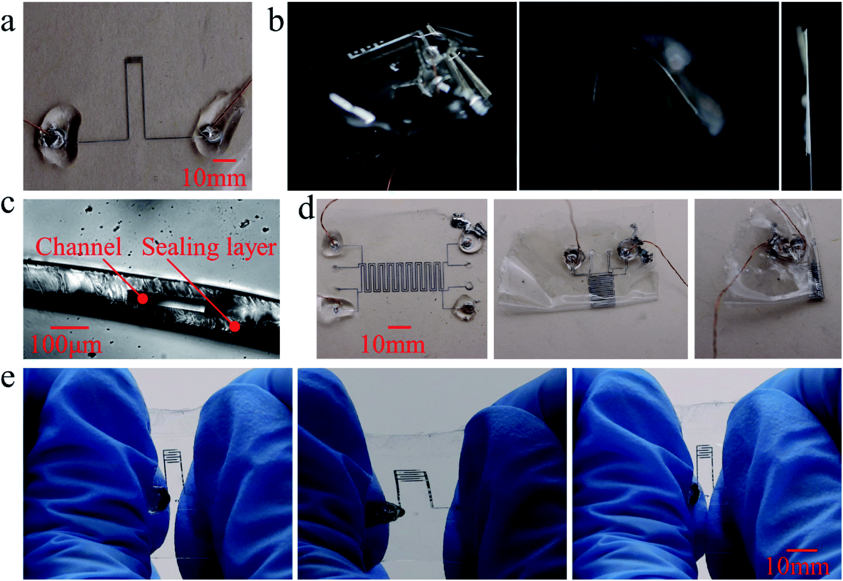 | ||
| Fig. 1 Fabricated microelectrode and its properties. (a) A thin liquid-metal-based flexible microelectrode; (b) side view and flexibility of the microelectrode (left and middle) and thickness comparison with an A4 paper (right); (c) thickness measurement under a microscope; (d) the flexible microelectrode be folded twice; (e) stretchability of microelectrode. | ||
In this work, an approach for fabricating thin liquid-metal-based microelectrodes with a reversible PC-bonding technique is introduced and is shown in Fig. 1(a). By applying the femtosecond laser to the thin membrane, a blind-end design for liquid metal becomes feasible. The whole structure is highly flexible (Fig. 1(b)), and the whole thickness of the sealed microelectrode is 119 micron (Fig. 1(c)). The microelectrode is highly flexible and could be easily folded at least twice (Fig. 1(d)), and shows a good stretchability (Fig. 1(e)). In this paper, the detailed fabrication process of the whole structure is introduced. The different drilling parameters of femtosecond laser on the PDMS membrane are tested and show several complicated structures achieved by this technique. Finally, a comb-shaped strain capacitor sensor is designed, fabricated, and tested for its wearable finger movement sensing behavior.
Material and methods
Here, the materials, machines involved, and fabrication process for developing thin PDMS microchannel structures are detailed. The materials used in this study include PDMS (Sylgard 184 silicone elastomer kit, DowCorning), PC membrane (Qinglai company, Guangzhou, China), Ga75.5In24.5 as a liquid metal alloy that has a melting point of 15.5 °C, and photoresist (SU8-2050, MicroChem). The machines employed for the fabrication process of microelectrode include plasma treatment machine (Yanzhao Technology, Tangshan, China) and femtosecond laser ablation beam machine (developed by Laboratory of Organic Nanophotonics and Key Laboratory of Photochemical Convention and Functional Materials, Technical Institute of Physics and Chemistry) same as the one used in the literature.36 The instruments involved for experimental procedures and data collection include a camera (EOS 90D, Canon), microscope (Z1, Zeiss Observer, Oberkochen, Germany), and LCR instrument to test the capacity of the wearable sensor (TH2817B, Tongji, Chang Zhou, China).The schematic for the fabrication process flow of thin microelectrode is shown in Fig. 2(a). A complete microelectrode includes two layers i.e., a channel layer and a sealing layer. At first, the channel layer used to shape liquid metal in the microelectrode is fabricated by spin coating PDMS on a silicon wafer that has a pre-fabricated photoresist mold. The mold used here is 31 μm high, over which the PDMS (10![[thin space (1/6-em)]](https://www.rsc.org/images/entities/char_2009.gif) :1 ratio) is spin coating at 1000 rpm for 65 s. After the spin coating process, the PDMS shows a thickness of 69 μm. Then, the coated wafer is baked at 75 °C for 2 hours to cure the PDMS completely. A piece of PC membrane with a thickness of 0.15 mm and an area large enough to cover the whole mold structure is oxygen plasma-bonded to the upper surface of the cured PDMS, after which a 10 minutes 95 °C baking is performed to further enhance the bonding strength. The PC and PDMS layers are then peeled off from the silicon wafer together. Owing to the support provided by the PC membrane, the molded thin PDMS structure is not subjected to deformation or breakage while peeling off. The inlets to insert liquid metal of microelectrode are made with a 1.2 mm-diameter puncher. Thus, the preparation of the channel layer of microelectrode is completed.
:1 ratio) is spin coating at 1000 rpm for 65 s. After the spin coating process, the PDMS shows a thickness of 69 μm. Then, the coated wafer is baked at 75 °C for 2 hours to cure the PDMS completely. A piece of PC membrane with a thickness of 0.15 mm and an area large enough to cover the whole mold structure is oxygen plasma-bonded to the upper surface of the cured PDMS, after which a 10 minutes 95 °C baking is performed to further enhance the bonding strength. The PC and PDMS layers are then peeled off from the silicon wafer together. Owing to the support provided by the PC membrane, the molded thin PDMS structure is not subjected to deformation or breakage while peeling off. The inlets to insert liquid metal of microelectrode are made with a 1.2 mm-diameter puncher. Thus, the preparation of the channel layer of microelectrode is completed.
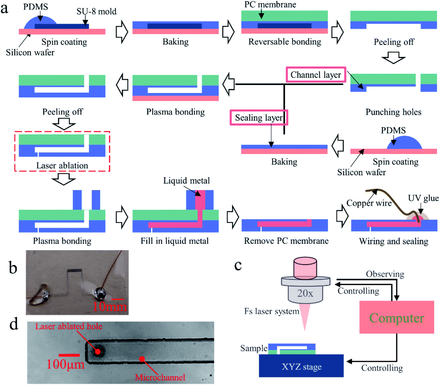 | ||
| Fig. 2 Fabrication process and the result of the microelectrode. (a) Schematic of the microelectrode fabrication process; (b) a photo of fabricated microelectrode; (c) schematic of laser drilling process during fabrication; (d) laser-drilled hole inside the microchannel. | ||
The sealing layer is used to seal the channel structure beneath the channel layer for which an empty PDMS membrane can be used. PDMS (10:1 ratio) is spin-coated on an empty silicon wafer with a speed of 2000 rpm for 65 s and baked at 75 °C for 2 hours. The spin-coated PDMS film has a thickness of 50 μm.
After the preparation of two different layers of microelectrodes, the next step is to attach the channel and sealing layer through bonding with the help of standard oxygen plasma treatment. Then all layers are peeled i.e., PC membrane, the channel layer, and sealing layer all together from the wafer. The support facilitated by the PC membrane makes this procedure feasible and keeps the structure intact. The laser ablation technique is used to drill a tiny hole at each blind-end of the channel which is discussed in detail in the upcoming section. The hole is drilled to the sealing layer i.e., the one without PC membrane. To maintain the stability of the femtosecond laser system, the whole laser ablation process is done in a room with constant temperature (22 °C) and humidity (45%). The laser spot size we used in this process, is 400–500 nm.
After laser ablation, the fabrication of the microelectrode structure is finished. The next step is to fill the liquid metal into the channel. GaIn liquid metal is chosen to inject into the channel structure directly by a syringe. However, as the structure is thin having a channel inlet height of only 42 μm, it is too thin for the syringe needle to stick stable enough to fill liquid metal inside the channel. Therefore, a thick-inlet is developed over the channel inlet for which a small PDMS block having a thickness larger than 1 mm is punched with a 2.0 mm diameter hole (large enough to support the syringe needle) and is bonded over the top PC membrane of thin microelectrode structure, making sure the larger hole fully covers the smaller channel inlet. The hole diameter of this thick block (2.0 mm) is designed larger than the inlet hole of the microchannel (1.2 mm) to simplify the aligning process. In the presence of thick PDMS block at channel inlet, liquid metal can be easily injected to form microelectrode. Due to large surface tension, the liquid metal would not flow through the small hole on the blind-end side of the channel but air would, and hence, liquid metal will be able to fill the whole microchannel. After injection, the PC membrane is removed from PDMS by the water treatment process presented in ref. 26, and therefore, both the PDMS block and PC membrane detach from thin PDMS microelectrode. The final step is to place a drop of liquid metal over the channel inlet and a thin copper wire is made to contact with the liquid metal droplet. This step ensures the connection between the copper wire and the inner liquid metal electrode. The electrode inlet and liquid metal drop are then sealed with fast-drying UV glue. The final structure of different channel designs is shown in Fig. 2(b).
The laser drilling process is an important step in the design of microelectrode. A facile schematic representation of the laser ablation/drilling process is shown in Fig. 2(c). After placing the sample on an XYZ stage, the focal length and the drilling position are adjusted by changing the sample XYZ stage position while observing through a computer. For drilling, the femtosecond laser beam is then emitted at the drilling position. In the present research work, the effect of different drilling periods is studied, and finally, optimized a reasonable emission time of 2 ms. The results concerning a detailed parametric study are discussed in the later section. The energy of the laser beam used for the present research is 295–330 mW. Fig. 2(d) shows a drilled hole inside the microchannel. The hole diameter is 25.96 μm and the drilling energy used is 307 mW.
Results
(a) Basic properties of this microelectrode
In the present work, a fabrication approach assisted with the femtosecond laser ablation technique for developing thin liquid-metal-based microelectrode is proposed. Optical images of developed thin microelectrode are shown in Fig. 1. Fig. 1(a) displays a blind-end comb microelectrode fabricated using the approach mentioned above. The fabricated system comprises a pair of electrodes, each of which has 3 side channels. The channel width obtained is 80 μm. While the system is lifted by a tweezer and seen from a side view, the microelectrode is found to be very thin with a high degree of flexibility and the thickness can be compared to that of one piece of A4 paper (Fig. 1(b)). The accurate thickness of this thin microelectrode is elucidated through the microscope (Fig. 1(c)) and the whole thickness of this microchannel structure is 119 μm with a 50 μm sealing layer and 69 μm channel layer. The channel height is 27 μm and the membrane above the channel is 42 μm thick with similar thickness to the sealing layer beneath the channel which provides enough protection to the molded liquid metal structure inside. Due to the liquid nature of liquid metal and the thin dimension of PDMS molds, the whole microelectrode has high flexibility and is soft enough to be folded at least twice (Fig. 1(d)). The high flexibility possessed by the microelectrode can be utilized in most applications related to soft electronics. Apart from flexibility, the thin microelectrode could be able to stretch over 1.7 times as shown in Fig. 1(e) which shows its potential to be used in the development of strain sensors or devices working under a high strain environment.(b) Parametric study of laser ablation time effects on hole size on the PDMS
The laser ablation technique is employed for making a hole in the blind-end to make it possible for the liquid metal injection inside the thin channels. To test the ability of the laser ablation technique to puncture the PDMS membrane, experiments are carried out with different membrane thicknesses ranging from 15 μm to 52 μm with different ablation times ranging from 1 ms to 1000 ms. The experiments are performed to elucidate the responses like whether the laser could drill through the PDMS membrane and how large the hole is. 7 different membrane thicknesses are used with 28 sets of ablation time (1–10 ms ranging by 1 ms, 20–100 ms ranging by 10 ms, and 200–1000 ms ranging by 100 ms) and therefore, 196 groups of experiments are performed. For each set of parameters, three holes are drilled and the final hole size is the average size of three holes. All the experiments are performed with an ablation energy of 330–331 mW. After each experiment, the drilled membrane is observed under a microscope and taken photographic images.The ablation results and statistical analysis of the laser ablation process with different parameters are shown in Fig. 3. Fig. 3(a) shows the result of one ablation test. The ablation parameters set for obtaining this result are a 15 μm thick membrane, 331 mW laser energy, and 400–700 ms ablation time from left to right.
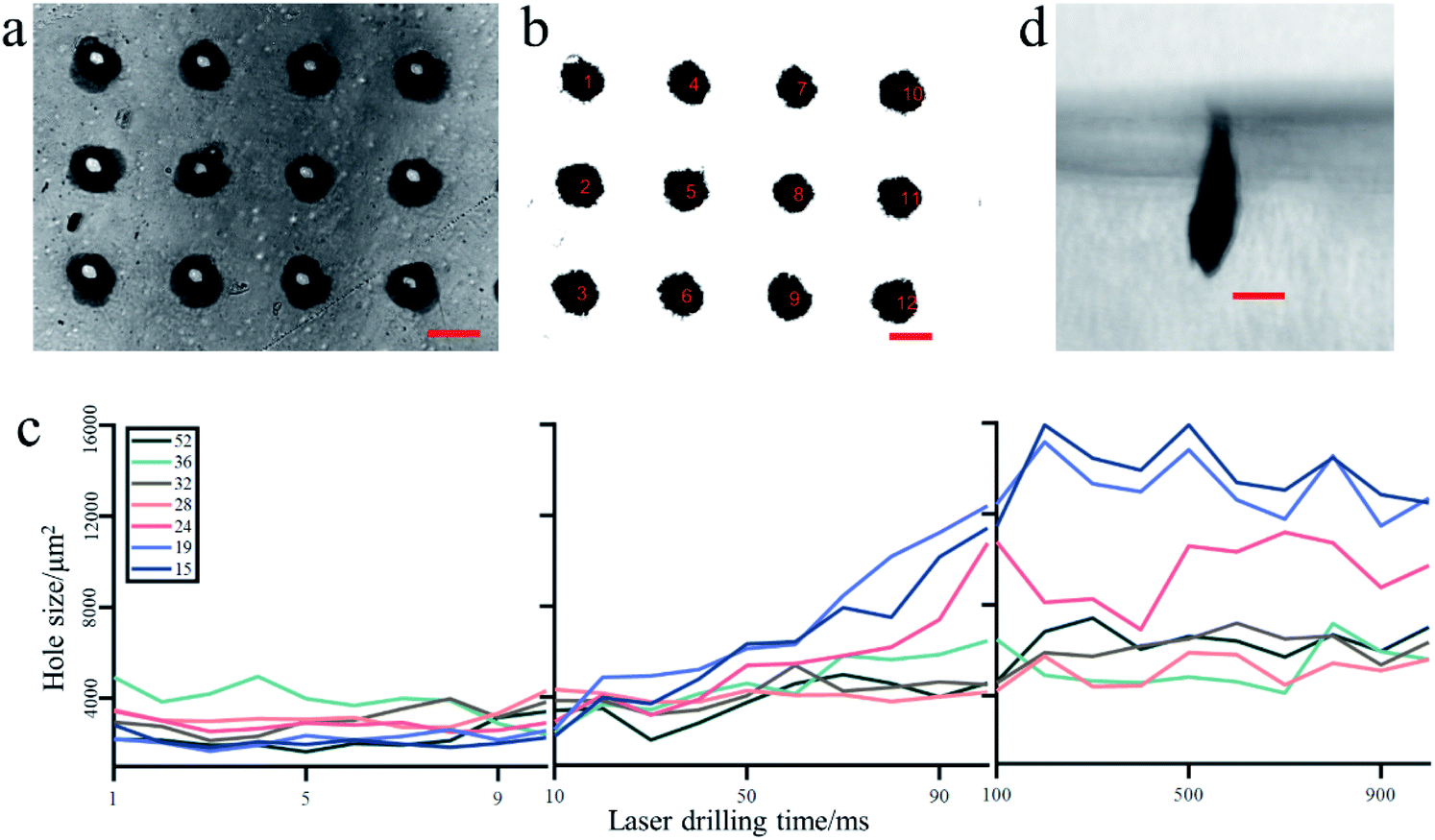 | ||
| Fig. 3 Experimental result and analysis of different laser drilling times on PDMS membrane. (a) Photo of patterned laser-drilled holes under a microscope; (b) extracted and numbered holes; (c) statistical result of laser-drilled hole sizes at different drilling times and different membrane thickness; figure legend represents different PDMS membrane thickness, and the unit is μm; (d) side view of the long-time drilled hole under a microscope. Scale bars in (a), (b) and (d) represents 5 mm. | ||
The hole size obtained for each set of ablation parameters is calculated. At first, the hole areas are segmented and repainted with black color as the one shown in Fig. 3(b). Then the holes are extracted and their boundaries are found. Because there is more than one hole in each image, holes are numbered from top to bottom and from left to right. The size of each hole is then calculated, averaged, and summarized in Fig. 3(c). Lines having different colors represent test results for different membrane thicknesses. As inferred from the figure, while the drilling time is within the range of 1–10 ms, not much difference in the hole size is seen. This might be because the 1 ms difference in drilling time is too small to see the difference. With the drilling time ranging from 20–100 ms, the hole size increases with the increase in drilling time. Higher drilling time i.e., more than 100 ms doesn't show much difference in hole size. A slight decrease of hole size is observed at 15 and 19 μm membrane thickness after 100 ms drilling time. This might be because the PC membrane under different drilling positions is slightly different, leading to different focal lengths at different drilling positions. However, the hole sizes are relatively stable compared with hole sizes under 100 ms drilling time. Membrane thickness of PDMS also affects the hole size where thinner membrane leads to larger hole size, especially concerning longer drilling time. However, with drilling time less than 10 ms, hole sizes don't show much difference with different membrane thicknesses.
Except for the drilling procedure at different drilling times, the present experiment also proves that PDMS membrane having a thickness less than 52 μm can be successfully drilled with 1 ms drilling time at 330 mW, and the drilling area does not change much with drilling time ranging from 1 to 10 ms.
The goal of using laser drilling for developing thin liquid metal microelectrode is to make blind-end design possible and also, it is designed in such a way that the liquid metal should not go through the drilled hole. Therefore, a smaller hole is expected in this design where the air can flow but not the liquid metal. According to the statistical results shown in Fig. 3(c), the hole size when drilled over 100 ms is 1–2 times larger than 1–10 ms drilled holes. So, in the following experiments, 1 ms or 2 ms is used as drilling time to avoid excessive drilling.
Apart from the short-time drilling ability, laser ablation on thick PDMS block with longer emission time is also tested. Fig. 3(d) shows the side view of the laser-ablated hole on a thick PDMS block with 20 s emission time and 330 mW emission energy. The achieved hole depth is 312 μm. This indicates that the laser drilling approach has the potential to make a drill in the thicker PDMS membrane or structure.
(c) Drilling position effects on liquid metal filling
The effectivity of the chosen parameter for laser drilling PDMS membrane is being proven in the present investigation. The next step towards the thin liquid metal microelectrode is to find a proper drilling position to make it easy for the liquid metal to fill the whole channel. Considering the compression of air in the channel, a hole at the end of the channel, might be the most effective approach. Here, an experiment is conducted to illustrate the influence of the drilling position on liquid metal filling.To conduct this experiment, a single microchannel with a length of 15.5 cm and 20 μm thick sealing layer is used. The channel has only one inlet and no outlet. Channel width is one of the parameters that need to be optimized for which 5 samples with different channel widths are prepared i.e., 100 to 500 μm, ranging by 100 μm. The whole channel has 20 turns, and the turnings are labeled one after the other. Overall, there are 10 labeled positions, as shown in Fig. 4(a). The last label is at the end of the channel. The distance between labeled positions to the inlet of the channel is 1.5 cm to 15.5 cm, increasing by 1.5 cm between the first 9 positions, and 2 cm between positions 9 and 10.
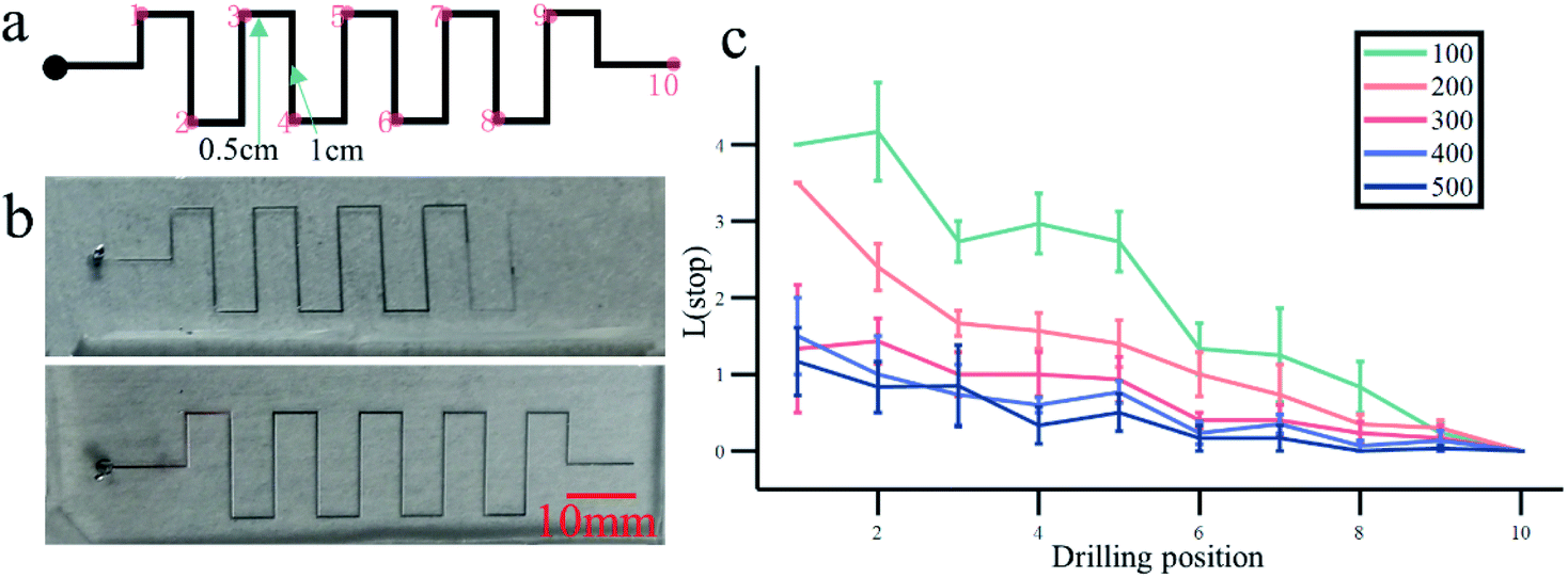 | ||
| Fig. 4 Experiment process and the result of laser drilling position. (a) Schematic representing the laser drilling position through numbering; (b) liquid metal filling result of two different drilling position: position 2 (top image) and position 10 (bottom image); (c) statistical result of drilling position and liquid metal filling result at different channel widths; error bar indicates the standard error at each point; figure legend represents different channel width, and the unit is μm. | ||
During the experiment, the femtosecond laser is used to drill at one of the 10 labeled positions. The laser energy used here is 307–309 mW. Each channel is drilled only with one hole. Then, the liquid metal is tried to fill from the inlet of the channel to check how long it would go inside the channel before being blocked. The filling is done with a syringe. Channel width is also an important parameter that influences the liquid metal filling. Therefore, 5 different widths for each drilling label are tested, and hence, 50 different chips are tested overall.
The furthest position liquid metal reaches in each test group is recorded and summarized. Fig. 4(b) shows the photographs of two different filling results. Here, the channel width is 200 μm where the drilling position is position 2 and position 10 in the top and bottom figure, respectively. Results depict that in the top figure of Fig. 4(b), liquid metal goes only until position 7.5 whereas, in the bottom figure, liquid metal fills the whole channel successfully. To optimize the filling condition, the length between the furthest position liquid metal reaches, and channel ends in each channel are recorded, where the furthest position indicates that liquid metal reaches before the membrane beneath the channel breaks. For example: in the channel shown in Fig. 4(b), the recorded position is 2.5 for the top image and 0 for the bottom image. For a simpler description, we describe the recorded position as marker ‘L(stop)’ in Fig. 4(c). Hence, the smaller the recorded position is, the better and further liquid metal fills the channels. The experiment is conducted three times for each channel length and drilling position, and the averaged L(stop) is calculated and recorded for each condition. Results obtained for all the 150 chips are summarized in Fig. 4(c) where the x-axis represents the drilling position and the y-axis is L(stop), and the error bar indicates the standard error at each data point. Five colored lines represent different channel widths used in the present study. Results show that when the drilling position is nearer to the end of the whole channel, the liquid metal goes further inside the channel. When drilling is done at position 10 i.e., the end of the channel, liquid metal fills the channel for all the five-channel widths. The influence of channel width concerning filling difficulty can be concluded as it is easier to fill a wider channel than a thinner channel. Therefore, while using the above process to make blind-end channels, it is enough to drill only one hole at the end of each channel to ensure the complete filling of liquid metal for the microelectrode. The goal for drilling holes in channels is to find an exit for air when we fill liquid metal in; it might be easier and faster for air to flow out if extra holes are drilled at the middle of the position of channels to ensure liquid metal filling but from the current study, it is not necessary.
Except for the drilling position, it might be a wonder how hole size affects the liquid filling process. From our experiment, we find that hole size has little influence on liquid metal filling. We fill liquid metal into channels, same as the ones used in Fig. 4, with different hole sizes, whose drilling times are 1 ms, 10 ms, 100 ms, and 1000 ms, respectively. Liquid metal is successfully filled into all these channels. The hole sizes are different in each group; however, liquid metal filling results are the same.
(d) Complicated microelectrode structures
Fig. 5 shows photographic images of some complicated microelectrode structures fabricated using the blind-end laser ablation technique. The microelectrodes shown in Fig. 5(a)–(f) are smaller electrodes but are not thin structures. However, Fig. 5(g) is a large-area, thin, and the most complicated microelectrode fabricated with a thickness of 119 μm. Here, the sealing layer for both thick and thin structures is 50 μm. For all the designs, there is only one inlet and there is no outlet. Small holes are drilled by a femtosecond laser at each channel end. The drilling position of each structure is marked with a small red dot on each photograph as depicted in Fig. 5(a) where a circle-ambulatory-plane antenna without branches. Here, the channel has one inlet at the outermost circle and one drilled hole at the innermost circle position marked with a red dot. For structures shown in Fig. 5(f) and (g), only a part of drilled positions is marked. As the structures are symmetrical and have lots of branches and channel ends, all unmarked ends are also drilled symmetrically. In some designs, detailed structure photos taken under a microscope are shown where the liquid metal fills all channels well.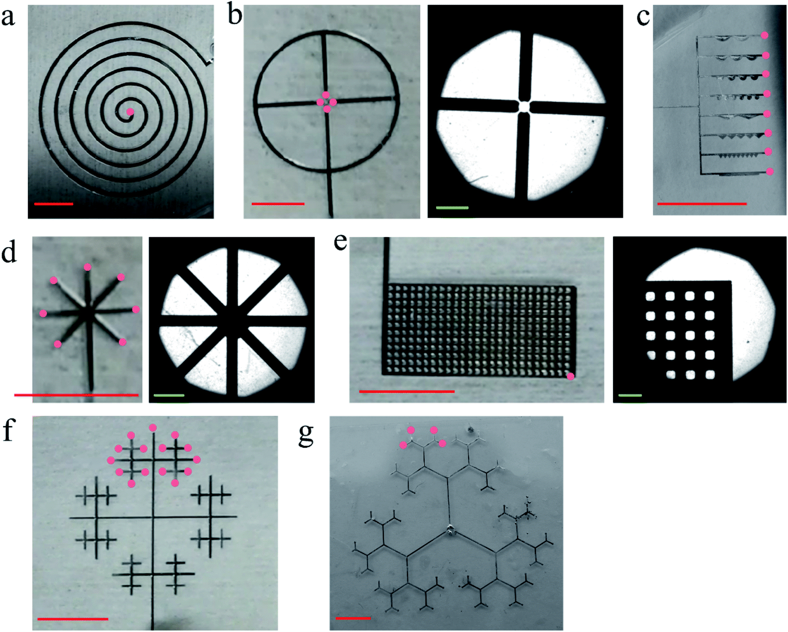 | ||
| Fig. 5 Photographs of some complicated microelectrodes. Red dots represent the position of laser drilling in each subfigure. (a) round antenna; (b) wheel design with four-channel ends and its detailed optical image; (c) detailed and small structure design with eight-channel ends; (d) multi bifurcation design and its detailed optical image; (e) large-area design and its detailed optical image; (f) complicated channel design with multi branches and channel ends; (g) thin snow-like design with multiple branches. Scale bars with red lines represent 5 mm, and green lines represent 500 μm. | ||
This section provides experimental confirmation about the stability and effectiveness of the laser drilling process for liquid metal electrode fabrication. The complicated and large structure shown in Fig. 5(g) is the design where laser ablation and thin fabrication process are involved. This structure has only one inlet in the middle of the structure. Three branches are then separated from the inlet hole and then, separated, again and again, finally leading to the construction of a complicated structure. The successful filling of liquid metal in the complicated structures makes it possible to be used in the construction of large-area, complicated, multi-branched, blind-end, and thin liquid metal microelectrodes.
(e) Application of thin flexible microelectrode: wearable stain sensor testing finger movement
To test the performance of the fabricated thin microelectrode in the realistic application, a capacitor strain sensor is developed with the thin microelectrode fabrication approach proposed in the present work. The sensor comprises a pair of comb-structure microelectrode arrays with more than 10 branches which are shown in Fig. 6(a).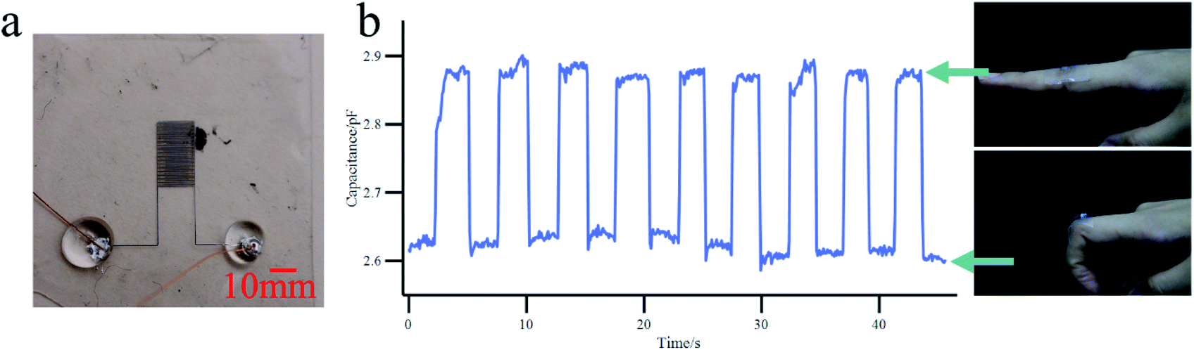 | ||
| Fig. 6 Application of thin liquid metal-based flexible microelectrode as a wearable strain sensor. (a) A photo of the come shape sensor; (b) measured capacitance at different finger positions. | ||
The sensor is tested as a wearable sensor for detecting finger movement. The sensor is worn on an index finger. Thanks to the thin structure of this sensor, it could stick to the skin by static electrical force, and no glue or other adherents are necessary. The sensor stays on the finger steadily owing to its flexibility and small thickness. The test is performed by moving the finger between two states i.e., straight and 90° as shown in the right images of Fig. 6(b). In the meanwhile, the capacitance between two electrodes is tested through an LCR instrument where the capacitance is collected at 50 kHz, 1 V voltage, and 5 data points per second.
The capacitance response of this wearable strain sensor is shown in the left image of Fig. 6(b). With finger movement, the sensor is deformed and strained. Correspondingly, the capacitance is changed between two different positions where the higher one represents the straight state of the finger and the lower capacitance represents 90°. This result indicates that the fabricated sensor is capable of detecting finger states and can be used as a wearable strain sensor. Moreover, this experiment substantiated the potential and effectiveness of the fabricated thin liquid metal microelectrodes for flexible electronics and wearable sensor applications owing to their high flexibility. The high degree of flexibility is due to the use of liquid metal and PDMS having relatively thin structures fabricated using the reversible PC membrane bonding process.
Wearable strain sensor has been a popular subject in soft electronics. Different from most strain sensors that need large structures like a glove, or adherents to fix the sensor on the skin, the stain sensor presented here could directly be fixed on the skin by statistical electric forces, and finish the sensing approach. Due to the thin structure of this sensor, it could fit different skin shapes and gestures, like the bending movement of the finger in Fig. 6. Besides, this application shows the potential of the approach proposed here, to work as a wearable sensor, to find its position in soft electronics and very thin electrical devices.
Conclusions
In the present work, an approach for fabricating high resolution, thin (119 μm), and blind-end liquid metal microelectrodes is proposed. The microelectrode is fabricated by injecting room temperature liquid metal into thin PDMS channels. The high resolution of the channels used to shape liquid metal is achieved by soft lithography. The thin electrode structure is developed with the assistance provided by the reversible PC membrane bonding process developed in our lab.26 Even though, there are several approaches reported for fabricating blind-end liquid metal electrode, the fabrication process and the thickness of the whole channel is found limited. In this regard, the present work deals with the use of the laser ablation technique to make small holes on the PDMS membrane that make the fabrication of blind-end liquid metal electrodes possible. The fabricated thin liquid metal electrode shows a high degree of flexibility that can withstand even after several folding. Also, it has a high strain withstanding ability, and hence, its potential for developing wearable sensors and flexible electronics is illustrated in the present work.Flexible microelectrodes have been a hot study topic for a long period, where liquid metal has been a commonly seen electrode material. To shape liquid metal, numerous researchers have mixed liquid metal with other particle materials or simply used liquid metal and dispersed them as nanoparticles using ultrasound for developing ink. The developed ink is either printed,37 transferred,38 or written39 in the required pattern with different approaches to form electrodes. Even though some of these electrodes show high flexibility, the printing resolution or fabrication complicity exists with this fabrication process. Microchannel has always been a good choice to develop liquid metal-based microelectrodes for more than 10 years. However, it is very difficult to fabricate a very thin microchannel structure, and hence, the flexibility of this type of electrode is limited.6,7 In the present work, these limitations are rectified and can fabricate liquid metal microelectrode with a thin structure, high resolution, and a simple and low-cost fabrication process. This approach is a new choice in the development of flexible microelectrode.
PDMS is a very common material that is used in flexible electronics. Its flexibility is found better when the thickness is small. To overcome the fragility of thin PDMS while removing from its molds, in some previous reports, soft membrane such as soluble PVA membrane is used to assist in removing the PDMS membrane from silicon wafer,40 where the thickness of a single layer structure is 30 μm (in the present work, it is 69 μm with higher microchannel) and the channel area is only 1 cm2 (9 cm2 in the present study). However, the PVA membrane is reported to be very soft, and therefore, during large-area fabrication, the soft structures are deformed. Consequently, the deformation also occurs to the PDMS membrane. In the present study, a PC membrane with a thickness of 1.5 mm is used. PC membrane is chosen as it has appropriate flexibility i.e., it is hard enough to support the large thin PDMS structure while peeling off and soft enough to ease the peeling process. After peeling off, the PC membrane removal procedure is even simpler for thin structures. Once in contact with water, the PC membrane is naturally released from PDMS without any applied force, and hence, the deformation or break of thin PDMS structure can be effectively avoided. For all the experimental set of conditions, the PC membrane assisted thin PDMS structure fabrication results in large and stable thin PDMS structures.
Blind-end design has always been an effective approach to reduce the microchannel size and increase the degree of freedom for channel design. In the present study, femtosecond laser ablation progress is employed to develop the blind-end design for liquid metal microelectrode fabrication. A hole is drilled by the femtosecond laser at the very end of every electrode channel and the average hole size made by laser ablation is tested to be ranging from 1500–3000 μm2 for the membrane having a thickness between 15 μm to 52 μm and the drilling time between 1 ms to 1000 ms. Due to the large surface tension of liquid metal, it doesn't flow through this hole at the pressure used to fill it inside microchannels. The femtosecond laser has been widely used in the microchannel fabrication process, but barely in liquid filling assistance. This new design is simple and effective in blind-end liquid metal electrode fabrication.
Soft electrodes are a very essential component for developing flexible electronics. The fabricated microelectrode is tested as a wearable finger movement sensor. Instead of using extra glue or adherents, statistical electrical force is enough for the sensor to fix on skin. This application presented in the article is just proof of the good performance or potential for this microelectrode to be used in real-time applications.
So far, there have been so many approaches to fabricate soft electronics, and none of them is perfect, so is this one. Even the fabrication process of the microchannel is simple, it does need a femtosecond laser to assist with the blind-end design. Compared with the soft lithography process, femtosecond laser might not be that commonly seen, so it might be hard to finish the whole process in some conditions. Moreover, because the whole structure is fabricated with PDMS, and they are very thin, the fabricated electrodes should be carefully preserved and gently used to prevent them from damaging or breaking. In the future, a tougher material could be expected.
Author contributions
Zi Ye: conceptualization, data curation, formal analysis, investigation, methodology, validation, writing-original draft, writing-review & editing; Qian Li: data curation, methodology, investigation; Renchang Zhang: methodology; Pan Zhang: data curation, validation; Lin Gui: conceptualization, funding acquisition, project administration, supervision, validation writing-review & editing.Conflicts of interest
There are no conflicts to declare.Acknowledgements
This work is supported by the National Key Research and Development Program of China (2019YFB2204903) and the Science and Technology Program from State Grid Corporation of China (No. 5700-202155453A-0-0-00).Notes and references
- J. Guo, Y. Yu, L. Cai, Y. Wang, K. Shi, L. Shang, J. Pan and Y. Zhao, Mater. Today, 2021, 44, 105–135 CrossRef CAS.
- J. Heikenfeld, A. Jajack, J. Rogers, P. Gutruf, L. Tian, T. Pan, R. Li, M. Khine, J. Kim, J. Wang and J. Kim, Lab Chip, 2018, 18, 217–248 RSC.
- A. Nathan, A. Ahnood, M. T. Cole, S. Lee, Y. Suzuki, P. Hiralal, F. Bonaccorso, T. Hasan, L. Garcia-Gancedo, A. Dyadyusha, S. Haque, P. Andrew, S. Hofmann, J. Moultrie, D. Chu, A. J. Flewitt, A. C. Ferrari, M. J. Kelly, J. Robertson, G. A. J. Amaratunga and W. I. Milne, Proc. IEEE, 2012, 100, 1486–1517 Search PubMed.
- F. Schmitt, O. Piccin, L. Barbé and B. Bayle, Front. Robot. AI, 2018, 5 DOI:10.3389/frobt.2018.00084.
- T. Someya, T. Sekitani, S. Iba, Y. Kato, H. Kawaguchi and T. Sakurai, Proc. Natl. Acad. Sci. U. S. A., 2004, 101, 9966–9970 CrossRef CAS PubMed.
- Y. L. Park, B. R. Chen and R. J. Wood, IEEE Sens. J., 2012, 12, 2711–2718 CAS.
- R. D. Ponce Wong, J. D. Posner and V. J. Santos, Sens. Actuators, A, 2012, 179, 62–69 CrossRef.
- T. Ha, J. Tran, S. Liu, H. Jang, H. Jeong, R. Mitbander, H. Huh, Y. Qiu, J. Duong, R. L. Wang, P. Wang, A. Tandon, J. Sirohi and N. Lu, Adv. Sci., 2019, 6(14) DOI:10.1002/advs.201900290.
- Y. Wang, Y. Qiu, S. K. Ameri, H. Jang, Z. Dai, Y. A. Huang and N. Lu, npj Flexible Electron., 2018, 2(1) DOI:10.1038/s41528-017-0019-4.
- B. Nie, R. Li, J. D. Brandt and T. Pan, Lab Chip, 2014, 14, 4344–4353 RSC.
- T. Guinovart, A. J. Bandodkar, J. R. Windmiller, F. J. Andrade and J. Wang, Analyst, 2013, 138, 7031–7038 RSC.
- R. K. Mishra, A. Martín, T. Nakagawa, A. Barfidokht, X. Lu, J. R. Sempionatto, K. M. Lyu, A. Karajic, M. M. Musameh, I. L. Kyratzis and J. Wang, Biosens. Bioelectron., 2018, 101, 227–234 CrossRef CAS PubMed.
- H. Jeong, T. Ha, I. Kuang, L. Shen, Z. Dai, N. Sun and N. Lu, Proc. Annu. Int. Conf. IEEE Eng. Med. Biol. Soc., 2017, 4094–4097 Search PubMed.
- L. Zhu, B. Wang, S. Handschuh-Wang and X. Zhou, Small, 2020, 16, 1–32 Search PubMed.
- R. Zhang, Z. Ye, M. Gao, C. Gao, X. Zhang, L. Li and L. Gui, Lab Chip, 2020, 20, 496–504 RSC.
- L. Zhang, M. Gao, R. Wang, Z. Deng and L. Gui, Sensors, 2019, 19(6) DOI:10.3390/s19061316.
- Q. Wang, Y. Yu, J. Yang and J. Liu, Adv. Mater., 2015, 27, 7109–7116 CrossRef CAS PubMed.
- M. Baharfar, M. Mayyas, M. Rahbar, F. M. Allioux, J. Tang, Y. Wang, Z. Cao, F. Centurion, R. Jalili, G. Liu and K. Kalantar-Zadeh, ACS Nano, 2021, 15, 19661–19671 CrossRef CAS PubMed.
- L. Johnston, J. Yang, J. Han, K. Kalantar-Zadeh and J. Tang, J. Mater. Chem. C, 2022, 10, 921–931 RSC.
- R. Guo, X. Sun, S. Yao, M. Duan, H. Wang, J. Liu and Z. Deng, Adv. Mater. Technol., 2019, 4, 1–11 Search PubMed.
- R. K. Kramer, C. Majidi and R. J. Wood, Adv. Funct. Mater., 2013, 23, 5292–5296 CrossRef CAS.
- L. Amato, S. S. Keller, A. Heiskanen, M. Dimaki, J. Emnéus, A. Boisen and M. Tenje, Microelectron. Eng., 2012, 98, 483–487 CrossRef CAS.
- J. B. Chossat, Y. Tao, V. Duchaine and Y. L. Park, Proc. - IEEE Int. Conf. Robot. Autom., 2015, 2015-June, 2568–2573 Search PubMed.
- J. Yin, V. J. Santos and J. D. Posner, Sens. Actuators, A, 2017, 264, 289–297 CrossRef CAS.
- K. Zheng, S. Chen, L. Zhu, J. Zhao and X. Guo, IEEE Electron Device Lett., 2018, 39, 424–427 CAS.
- J. Hong, J. Gong, Q. Li, Z. Deng and L. Gui, Lab Chip, 2021 10.1039/d1lc00726b.
- Z. Ye, R. Zhang, M. Gao, Z. Deng and L. Gui, Micromachines, 2019, 10, 1–10 Search PubMed.
- K. Khoshmanesh, S. Y. Tang, J. Y. Zhu, S. Schaefer, A. Mitchell, K. Kalantar-Zadeh and M. D. Dickey, Lab Chip, 2017, 17, 974–993 RSC.
- R. Wang, L. Gui, L. Zhang, Z. He, M. Gao, S. Chen, X. Zhou, Y. Cui and Z. Deng, Adv. Mater. Technol., 2019, 4, 1–8 Search PubMed.
- V. Bharambe, D. P. Parekh, C. Ladd, K. Moussa, M. D. Dickey and J. J. Adams, Addit. Manuf., 2017, 18, 221–227 CAS.
- X. Zhu, Microsyst. Technol., 2009, 15, 1459–1465 CrossRef CAS.
- B. Bin Xu, Y. L. Zhang, H. Xia, W. F. Dong, H. Ding and H. B. Sun, Lab Chip, 2013, 13, 1677–1690 RSC.
- G.-L. Roth, C. Esen and R. Hellmann, Opt. Express, 2017, 25, 18442 CrossRef CAS PubMed.
- Z. Y. Hong, K. Okano, D. Di Carlo, Y. Tanaka, Y. Yalikun and Y. Hosokawa, Sens. Actuators, A, 2019, 297, 111566 CrossRef CAS.
- C. Chen, L. A. Shi, Z. Huang, Y. Hu, S. Wu, J. Li, D. Wu and J. Chu, Adv. Mater. Interfaces, 2019, 6, 1–9 CrossRef.
- A. Wang, L. Jiang, X. Li, Y. Liu, X. Dong, L. Qu, X. Duan and Y. Lu, Adv. Mater., 2015, 27, 6238–6243 CrossRef CAS PubMed.
- L. Zhou, J. Fu, Q. Gao, P. Zhao and Y. He, Adv. Funct. Mater., 2020, 1906683 CrossRef CAS.
- M. Kim, H. Alrowais, S. Pavlidis and O. Brand, Adv. Funct. Mater., 2017, 27, 1604466 CrossRef.
- Y. Gao, H. Li and J. Liu, PLoS One, 2012, 7(9) DOI:10.1371/journal.pone.0045485.
- J. M. Karlsson, T. Haraldsson, C. F. Carlborg, G. Stemme and W. Van Der Wijngaart, 14th Int. Conf. Miniaturized Syst. Chem. Life Sci. 2010, MicroTAS 2010, 2010, 2, pp. 1202–1204 Search PubMed.
| This journal is © The Royal Society of Chemistry 2022 |