DOI:
10.1039/D1RA09392D
(Paper)
RSC Adv., 2022,
12, 19359-19374
Design optimization and efficiency enhancement of axial junction nanowire solar cells utilizing a forward scattering mechanism
Received
28th December 2021
, Accepted 27th June 2022
First published on 4th July 2022
Abstract
We report the design, optimization, and performance analysis of three axial junction nanowire solar cells (NW SCs) based on cadmium telluride (CdTe), copper indium gallium selenide (CIGS), and copper zinc tin sulfide (CZTS) with significant improvement in their optical and electrical characteristics compared to their planar counterparts. It is shown that the performance of these NW SCs can be further improved by incorporating a hemispherical indium doped tin oxide (ITO) forward scatterer on top of the ITO front contact of the solar cells. We also compare forward scatterer incorporated NW SCs with forward scatterer incorporated planar solar cells (PSCs) and observe that forward scatterers significantly enhance the absorption in both cases. We further study the optimum size and arrangement of ITO hemispheres that result in improved photocurrent. In optimum cases, the incorporation of forward scatterers leads to absorption enhancement of 7.8%, 5.36%, and 8.8% in PSCs, and 21.4%, 7.36%, and 6.02% in NW SCs, respectively, for CdTe, CIGS, and CZTS absorbers in the same order. From the absorption profile at various wavelengths, it is found that forward scatterers enhance absorption in the 450–600 nm wavelength range, while nanowires improve absorption in the 600–800 nm range, and their combination results in an improved absorption profile for the entire visible wavelength range. We also observe increased electron–hole-pair (EHP) generation rate due to increased field-scattering and light concentration at the center of the nanowire below forward scattering hemispheres, leading to 46%, 32%, and 82.5% improvement in power conversion efficiency (PCE) for the three absorber layers, respectively. The effects of Al2O3 and SiO2 passivation layers surrounding the nanowires of the optimized cells are observed, and we conclude that the CIGS absorber benefits the most when the SiO2 passivation layer is used, increasing its PCE from 29.72% to 32.43%, while the PCEs of CdTe and CZTS are unaffected by the passivation layer due to competing effects of reduced absorption and reduced surface recombination.
1. Introduction
Solar energy holds the key to a future powered entirely by renewable energy sources. Despite extensive research, solar cells continue to trail traditional fuel sources, owing to their greater cost per Watt peak.1 As a result, lowering the cost of solar cells while increasing their efficiency has been a major concern. Solar cells based on nanostructures have the potential to address this issue in a variety of ways. One approach is to use nanostructures such as nanospheres or nanorods to improve the absorption of planar solar cells via scattering and field enhancement through plasmon resonance or dielectric scattering.2–5 In another approach, the absorber layer can take the form of nanorods or nanopillars, resulting in NW SCs.6–9 Nanowires have superior optical, electrical, and mechanical properties due to their higher surface-to-volume ratio and smaller dimensions, making them ideal for solar cell applications.10
Three-dimensional structures show improved light absorption11–16 due to reduced reflection,12,17,18 light-concentration,19 wave-guiding effects,20 and resonance described by Mie theory.5,21,22 The reflection suppression achieved via scattering19,23 among neighboring nanostructures eliminates the need for conventional anti-reflection coating. NWs also favor elastic strain relaxation due to their geometry and free lateral surface, which prohibits the formation of dislocations. As a result, defect-free NWs can be grown on lattice-mismatched substrates14,24,25 allowing for a wide range of material choices for achieving optimum bandgaps.26 This can reduce production costs by allowing NW growth on earth-abundant substrates through bottom-up (e.g., vapor–liquid–solid process) or top-down (such as chemical etching) approaches. Furthermore, the aerotaxy (gas-phase epitaxy) method has been shown to be capable of fabricating nanowires without the usage of any substrate.27–29 NW SCs can play a significant role in powering modern, flexible electronic devices due to their inherent mechanical flexibility and ability to be fabricated on flexible substrates.30–32 Another advantage of NW SCs is their radiation tolerance, which makes them well-suited for space applications.33
In NW SCs, the p–n junction can be grown either radially around the axis, or axially along the length of the nanowire, giving rise to radial junction and axial junction NW SCs, respectively. Radial junction NW SCs have the added advantage of improved carrier collection due to the orthogonalization of charge carrier generation and collection directions, which makes them particularly useful for materials with very short minority carrier diffusion length.6,19,34,35 Despite their advantage, radial junction NW SCs lag behind their axial junction counterparts when traditional highly crystalline materials are used. Most of the research on axial junction NW SCs so far has been focused on III-V materials, with the highest recorded efficiency of 17.8% for InP36 and 15.3% for GaAs.37 These values indicate a large gap that still exists between experimental values and the Shockley–Queisser limit of 33.7% efficiency.38 Hence, there is still a need to search for various materials and approaches to improve the performance of NW SCs. One such approach capable of improving NW SC efficiency could be the usage of forward scatterers at the front surface of these cells.
ITO is being widely used as the transparent top contact of various solar cells due to its improved electrical and optical properties. Studies have shown that solar cells with textured ITO contact have better photocurrent due to forward Mie scattering than those with planar ITO contact.36,39 For PSCs, nanostructures on the surface result in improved absorption via reflection suppression, whereas for NW SCs forward scattering couples with light concentration effects. Using these forward scatterers in conjunction with absorber materials like CdTe, CIGS, and CZTS, the performance of NW SCs may be considerably improved. CdTe and CIGS based thin-film solar cells are the most promising contenders of Si for commercial large-scale solar module production.40,41 This is due to their direct bandgaps and high absorption coefficients, which allow for the use of a very thin absorber layer, considerably lowering production costs. So far, the highest reported efficiency values for these cells are 22.1% for CdTe42 and 23.35% for CIGS,43 respectively. CZTS, known as Kësterite, is another exciting material for low-cost solar cell production due to its earth-abundant non-toxic constituents and near-optimum bandgap of 1.4–1.6 eV. However, its efficiency is still relatively low, with 11.01% as the maximum reported efficiency.44 CdTe-based nanopillar radial junction solar cells with a conversion efficiency of 1.06% were initially reported in the literature utilizing a CdTe nanorod//poly(3-octylthiophene) composite layer by Kang et al.45 Other hybrid radial junction solar cells employing CdTe with nanowires composed of ZnO46 or TiO2![[thin space (1/6-em)]](https://www.rsc.org/images/entities/char_2009.gif) 47 have been developed since then. CIGS and CZTS nanowires in conjunction with Si48 or ZnO48,49 have also been reported. On the other hand, axial junction solar cells based on CdTe, CIGS and CZTS have not been explored yet. The promise of decreased costs by using these widely studied materials with inexpensive earth-abundant constituents coupled with the advantages of nanowires can represent sustainable technological enhancement for affordable solar power harvesting. This might be a challenge for nanowire solar cells made with other novel materials with limited availability.
47 have been developed since then. CIGS and CZTS nanowires in conjunction with Si48 or ZnO48,49 have also been reported. On the other hand, axial junction solar cells based on CdTe, CIGS and CZTS have not been explored yet. The promise of decreased costs by using these widely studied materials with inexpensive earth-abundant constituents coupled with the advantages of nanowires can represent sustainable technological enhancement for affordable solar power harvesting. This might be a challenge for nanowire solar cells made with other novel materials with limited availability.
One limiting factor of thin-film solar cell efficiency is the surface recombination arising from lattice mismatch and dangling bonds between the absorber and surrounding layers.50,51 This presents the need for surface passivation.52–54 Front and rear surface passivation of CdTe, CIGS and CZTS solar cells have been shown to have significant impacts on the open-circuit voltage and efficiency of these cells.55,56 Al2O3 and SiO2 are two of the most investigated materials used for the passivation of these cells due to their superior properties and the technological feasibility of using them for passivation using several processes including chemical bath deposition, gas phase epitaxy and sputtering.53,55–66 For nanowire solar cells, the enhanced surface area that improves utilization of solar spectrum also presents the challenge of enhanced surface recombination resulting in deterioration of external quantum efficiency of the solar cell due to lost charge carriers at the surface.67 Surface passivation is needed for the alleviation of surface recombination which can significantly improve the carrier collection efficiency.
Considering the above, we have explored the potential of CdTe, CIGS, and CZTS-based axial junction NW SCs in this work. We have optimized their designs incorporating forward scattering ITO hemispheres and compared their performances with those of planar cells using optoelectronic simulations. The effects of Al2O3 and SiO2 passivation layers (PLs) on the optical and electrical properties of the optimized solar cells have also been examined. Following section describes the device structures, optoelectronic simulation model, and figures of merit used to compare the solar cells. The simulation results are discussed and analyzed in the results and discussion section. Finally, the conclusion section summarizes the findings of this study.
2. Device design and modeling
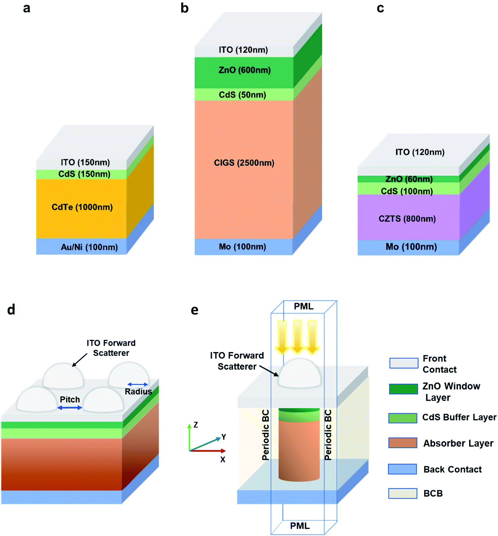
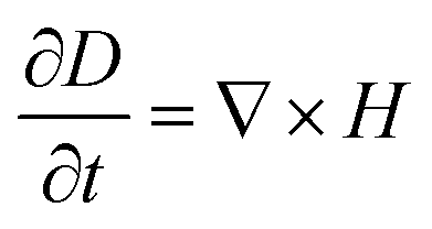
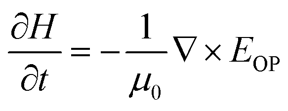
The effect of nanowires and forward scatterers were studied by comparing their performances with those of planar solar cells, the structures of whom were taken from experimentally reported devices.68–74 Fig. 1a–c depict the studied structures of CdTe, CIGS, and CZTS planar solar cells used as reference for comparison. In the layouts, CdTe, CIGS, and CZTS represent the p-type absorber layer. The thin CdS layer acts as the buffer layer in these cells. CIGS and CZTS cells have an additional window layer of ZnO. Both CdS and ZnO are n doped. The back contact is made up of Au/Ni combination for CdTe cell and Mo for CIGS and CZTS cells. The front contact of all the cells consists of the transparent conductive electrode of ITO. We then studied the effects of placing ITO forward scattering hemispheres on top of the PSCs and NW SCs. Fig. 1d and e depict the structure of planar and nanowire solar cells with ITO scatterers, respectively. The absorber, buffer, and window layers are axially stacked to form the nanopillar in the NW SCs.
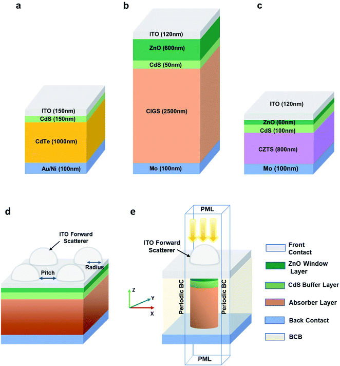 |
| | Fig. 1 Device structures of (a) CdTe,68,69 (b) CIGS,70–72,74 and (c) CZTS73 solar cells. (d) Planar solar cell with ITO forward scatterers. (e) Optical simulation unit of NW SC with forward scatterers (PML = Perfectly Matched Layer, BC = Boundary Condition, BCB = benzocyclobutene). | |
The nanopillars are arranged in square arrays in the solar cell structure and space between them is filled with benzocyclobutene (BCB), a polymer with an effective refractive index of 1.5. The polymer also performs the planarization of the cell. Through the ITO contact, the top surfaces of all the nanowires are linked. As far as the experimental viability of the proposed design is concerned, fabrication of GaAs and InP axial junction NW SCs with hemispherical ITO particles as forward scatterers has been demonstrated previously.36,75
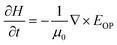
The performance of the solar cells was analyzed through optical and electrical stimulations. For optical simulation, three-dimensional finite difference time domain (FDTD) method was used. The solar cells were modeled using complex refractive index (ε(λ) = n(λ) + jk(λ)) of each layer, where ε, n, and k are the dielectric permittivity, refractive index, and extinction coefficient, respectively. AM 1.5G standard solar spectrum was used to model the perpendicularly incident solar irradiance. The computational domain and its boundary conditions are shown in Fig. 1e for the NW SC. Periodic boundary conditions were used along the horizontal dimensions due to the symmetry of the cell, whereas perfectly matched layers (PML) were placed at the top and bottom to avoid any reflection. Similar boundary conditions were employed for the PSCs with and without forward scatterers.
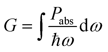
The FDTD simulator (implemented using ANSYS Lumerical in this work) is based on the simultaneous time-dependent solution of Maxwell's third and fourth equations, which are given by
| |
 | (1) |
| |
 | (2) |
Here, EOP is the optical electric field inside the structure, D is the displacement vector, H is the magnetic field intensity, ω is the angular velocity, ε0 is the permittivity of free space and εr is the relative permittivity of the material under consideration (ε = ε0εr). The electric field was obtained by simultaneously solving eqn (1) and (2), from which the optical power absorbed (Pabs) is calculated. The absorbed irradiance gives rise to electron–hole pair (EHP) generation measured by the generation rate (G),
| | |
Pabs(x, y, z, ω) = −0.5ω|EOP|2 × imag(ε)
| (3) |
| |
 | (4) |
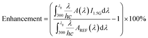
From the optical simulation results, we calculated the space integrated absorbed power A(λ) (λ representing wavelength) from reflection (R(λ)) and transmission monitor (T(λ)) data. Then, we evaluated the optical performance of various cells with respect to PSCs by using the following enhancement parameter based on the integrated quantum efficiencies of respective cells.
| | |
A(λ) = 1 − R(λ) − T(λ)
| (5) |
| |
 | (6) |
Here, AREF(λ) represents the integrated absorbed power for reference optimized planar solar cell. I1.5G is the AM 1.5G standard solar radiation and λg represents the wavelength corresponding to the bandgap of absorber material, beyond which absorption in a solar cell is negligible.
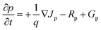
2D-axisymmetric simulation was performed to calculate the photocurrent (Jph) and other solar cell parameters by solving the drift-diffusion equations [eqn (7) and (8)], continuity equations [eqn (9) and (10)] and Poisson equation [eqn (11)], self-consistently.
| |
 | (9) |
| |
 | (10) |
| | |
−∇εE = E(p − n + Na − Nd)
| (11) |
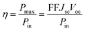
Here, Jn and Jp represent the current density due to electrons and holes, respectively. Rn(Rp) and Gn(Gp) are the recombination and generation rates for electrons (holes). p, n, Na and Nd are the hole, electron, acceptor, and donor concentrations, respectively. COMSOL Multiphysics Semiconductor module76 was used for obtaining the J–V characteristics of the solar cells by self-consistently solving eqn (7)–(11), using the Generation rate (G = Gn/Gp) imported from the optical simulation results of the FDTD solver and recombination rates obtained from literature. The addition of the PL has been modeled as a reduction in surface recombination velocity.52,53,62,77 The power conversion efficiency (η) and other parameters of interest were obtained from the J–V characteristics of the cell as follows:
| |
 | (12) |
where,
Jsc is short circuit current density,
Voc is the open circuit voltage, and FF is the fill factor.
Pmax is the output power of the solar cell at the maximum power point, while
Pin is the input power which represents the power of AM 1.5G solar spectrum.
3. Model verification
In order to verify the accuracy of our methodology, we first simulated planar cells with different absorber layers and benchmarked our simulation model and parameters. The performances of the simulated devices were compared with experimentally reported CdTe,78 CIGS,70 and CZTS79 cells. The electrical parameters used in simulation are listed in Table 1.62,68,73,80–95 Optical parameters such as refractive index (n) and extinction coefficients (k) were also taken from the literature.68,73,96 Table 2 represents a comparison between experimental reference cells and our simulated results, which are in good agreement with 2.94%, 1.918%, 1.63% relative error in efficiency for CdTe, CIGS, and CZTS, respectively. The verity of our method is also evident from the J–V curves shown in Fig. 2a–c. The benchmarked model parameters were used for the simulation and optimization of planar and nanowire cells with forward scatterers. The results of these simulations and optimizations were analyzed by comparing them to the respective benchmarked planar cell, which acted as the reference.
Table 1 Electrical parameters used in simulation
| Features |
CdTe68,80–82,97 |
CIGS83–87 |
CZTS73,88,89 |
CdS68,80,90,94 |
ZnO89,93,94 |
| Bandgap (eV) |
1.45 |
1.3 |
1.5 |
2.45 |
3.4 |
| DC permittivity |
10 |
13.6 |
10 |
10 |
9 |
| Electron affinity (eV) |
4.3 |
4.5 |
4.58 |
4.5 |
4.55 |
| Electron mobility (cm2 V−1 s−1) |
50 |
100 |
50 |
50 |
50 |
| Hole mobility (cm2 V−1 s−1) |
30 |
25 |
20 |
20 |
20 |
| NC (cm−3) |
1.3 × 10¹⁸ |
2.2 × 10¹⁸ |
2.2 × 10¹⁸ |
1.8 × 10¹⁹ |
4 × 10¹⁸ |
| NV (cm−3) |
7.6 × 10¹⁸ |
1.8 × 10¹⁹ |
1.8 × 10¹⁹ |
1.5 × 10¹⁸ |
9 × 10¹⁸ |
| NA (cm−3) |
1 × 10¹³ |
1 × 10¹⁵ |
5 × 10¹⁴ |
— |
— |
| ND (cm−3) |
— |
— |
— |
1 × 10¹⁷ |
5 × 10¹⁴ |
| SRH recombination lifetime, (ns) |
10 |
10 |
0.27 |
0.75 |
0.5 |
| Direct recombination factor (EHP capture rate cm3 s−1) |
3 × 10⁻¹⁰ |
2 × 10⁻¹⁰ |
3 × 10⁻¹⁰ |
2–6 × 10⁻¹⁰ |
2–3 × 10⁻¹⁰ |
| Bandgap (eV) |
1.45 |
1.3 |
1.5 |
2.45 |
3.4 |
| Surface recombination velocity (cm s−1) |
104 to 105 |
104 to 105 |
104 to 105 |
— |
— |
Table 2 Comparison of simulated results with reference
| Absorber layer |
Parameter |
Simulation |
Experimental |
| CdTe78 |
Jsc (mA cm−2) |
28 |
28.56 |
| Voc (volts) |
0.84 |
0.8524 |
| η |
18.12% |
18.67% |
| FF |
77% |
76.69% |
| CIGS70 |
Jsc (mA cm−2) |
38.85 |
38.9 |
| Voc (volts) |
0.732 |
0.74 |
| η |
22.5% |
22.94% |
| FF |
79.1% |
79.68% |
| CZTS79 |
Jsc (mA cm−2) |
19.93 |
19.7 |
| Voc (volts) |
0.65 |
0.658 |
| η |
8.46 |
8.6% |
| FF |
65.2% |
66.3% |
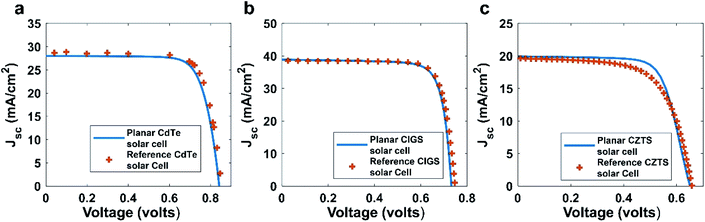 |
| | Fig. 2 Benchmarking of J–V characteristics of (a) CdTe, (b) CIGS, and (c) CZTS planar solar cells. The blue lines indicate results obtained from our simulation model, and red markers represent reference J–V characteristics extracted from reported studies in the literature. | |
4. Results and discussion
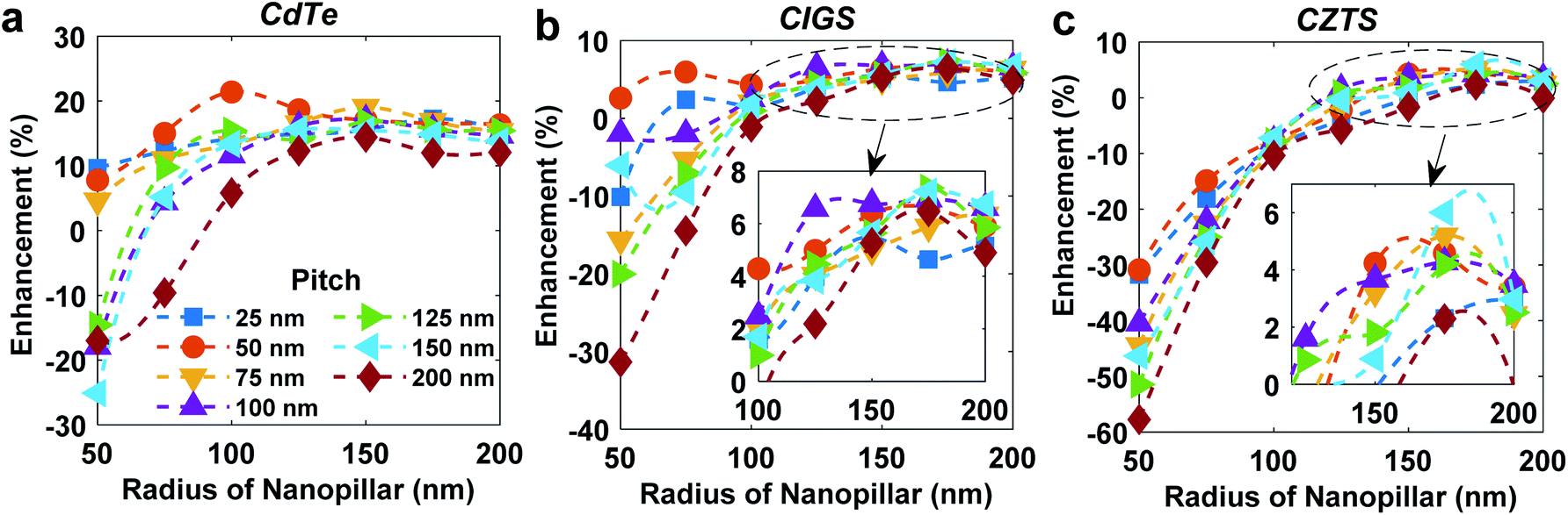
The dimensions of forward scatterer and nanopillars have been optimized to maximize the optical absorption in the solar cells. The effects of these optimizations on optical and electrical parameters are reported in this section. During the optimization, the lengths of all the PSCs or NW SCs were kept constant at the value of reference solar cell for rational comparison. The optimum sizes of hemispheres and nanopillars for different absorbers in terms of radius (r) and pitch (p, the shortest distance among adjacent hemispheres or nanopillars) are tabulated in Table 3, along with corresponding absorption enhancement values. The results are also illustrated in Fig. 3–6.
Table 3 Dimensions for optimum absorption enhancement
| |
Material |
Optimum radius (nm) |
Optimum pitch (nm) |
Enhancement (%) |
| Planar solar cell with forward scatterers |
CdTe |
175 |
75 |
7.8 |
| CIGS |
150 |
100 |
5.36 |
| CZTS |
175 |
75 |
8.8 |
| Bare nanowire solar cell |
CdTe |
100 |
50 |
15.1 |
| CIGS |
75 |
50 |
3.01 |
| CZTS |
175 |
150 |
−0.72 |
| Nanowire solar cell with forward scatterers |
CdTe |
100 |
50 |
21.4 |
| CIGS |
175 |
125 |
7.36 |
| CZTS |
175 |
150 |
6.02 |
| Decoupled enhancement for nanowire solar cell with forward scatterers |
CdTe |
125 |
75 |
5.7 |
| CIGS |
175 |
50 |
5.2 |
| CZTS |
150 |
50 |
8.01 |
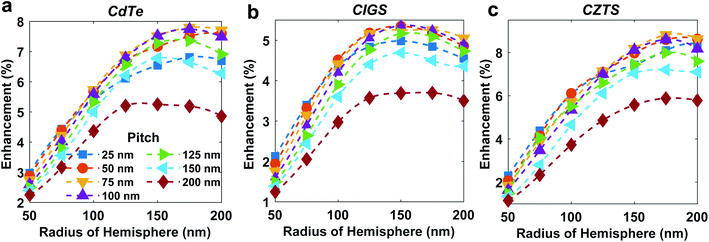 |
| | Fig. 3 Absorption enhancement for forward scatterer incorporated (a) CdTe, (b) CIGS, and (c) CZTS planar solar cells with respect to corresponding reference cells. | |
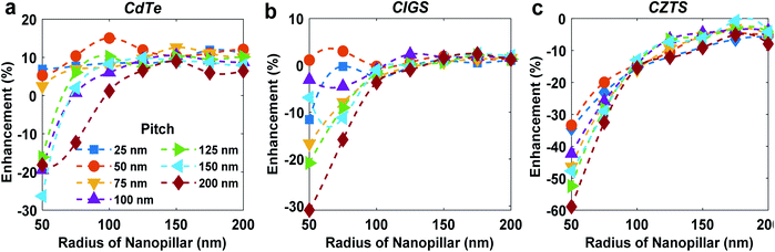 |
| | Fig. 4 Absorption enhancement for bare (a) CdTe, (b) CIGS, and (c) CZTS nanowire solar cells with respect to corresponding reference cells. | |
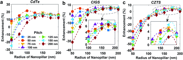 |
| | Fig. 5 Coupled absorption enhancement for forward scatterer incorporated (a) CdTe, (b) CIGS, and (c) CZTS nanowire solar cells with respect to corresponding reference cells. | |
 |
| | Fig. 6 Decoupled absorption enhancement for forward scatterer incorporated (a) CdTe, (b) CIGS, and (c) CZTS NW SCs with respect to corresponding bare NW SCs. | |
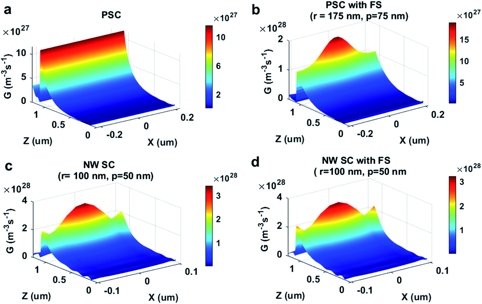
Fig. 3a–c show the optical absorption enhancement parameter (eqn (6)) variation with forward scatterer radius for various pitch values of CdTe, CIGS, and CZTS planar solar cells, respectively. The maximum absorption enhancement is 7.8% for CdTe PSC, 5.36% for CIGS PSC, and 8.8% for CZTS PSC. Mie theory suggests that for spherical nanoparticles, the scattering cross-section increases with particle dimension.98 This increased scattering results in an enhanced optical electric field, which improves optical power absorption. As a result, the absorption enhancement increases with increasing radius and reaches an optimum value for all the absorbers. The optimum radius is 175 nm for both CdTe and CZTS solar cells and 150 nm for CIGS solar cells, with the optimum pitch falling in the 75–100 nm range. Absorption decreases beyond the optimum radius because the light intensity reaching the absorber layers is reduced due to the existence of large hemispheres on top of a partially transparent front contact.
For NW SC, the optimum dimension at which optical absorption reaches the maximum value significantly varies for different absorber layers, which is evident from Fig. 4a–c. Negative enhancement implying a reduction in absorption at smaller radiuses for large pitch values is due to the absence of sufficient absorber material, which counteracts any benefit from field enhancement mechanisms. CdTe cell benefits the most from nanowire configuration with a 15.1% improvement in absorption (Fig. 4a). Enhancement for CZTS NW SC remains negative throughout the entire range of simulation values (Fig. 4c). The dimension (r = 175 nm, p = 150 nm) at which absorption of CZTS NW SC becomes equal to the PSC value has a volume filling factor of only 38.5%, indicating that the nanowire requires almost three times less material than the PSC for similar absorption. Hence the advantage of nanowire structure persists for CZTS solar cells due to lower material requirements.
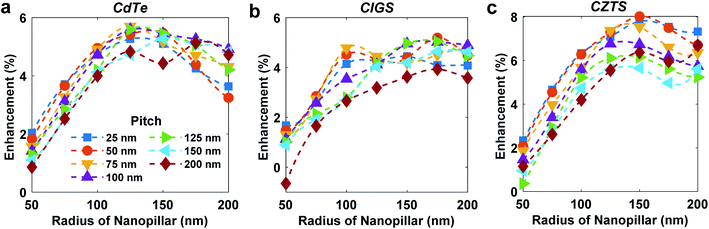
The effect of forward scatterer incorporation on NW SCs was also studied via simulation. However, the dimension of the ITO hemisphere for NW SCs was fixed by the underlying nanopillar's dimension since the hemisphere radius and pitch were kept equal to the corresponding parameters of NW SC. For these cells, two different mechanisms (forward scattering due to ITO hemispheres and light concentration due to nanowires) contribute to absorption enhancement; hence two different enhancement parameters are considered. The coupled enhancement parameter (Fig. 5a–c) represents the enhancement due to the combined effects of forward scatterers and nanowires. The improvement due to ITO hemisphere incorporation in these cells decoupled from the advantage of nanowire structures can be observed in Fig. 6a–c, which show the decoupled enhancement of NW SCs with forward scatterers with respect to the respective bare NW SCs.
The coupled enhancement (Fig. 5a–c) resembles the enhancement of bare NW SCs (Fig. 4a–c) with an upward shift. A maximum 21.4% coupled absorption enhancement is found for CdTe NW SC with forward scatterer (Fig. 5a) at a dimension (r = 100 nm and p = 50 nm) which coincides with the dimension for peak enhancement of bare CdTe NW SC (Fig. 4a). Fig. 6a shows that the decoupled enhancement is maximized around 5.7% (r = 125 nm, p = 50–100 nm) for CdTe NW SC. The pitch that results in maximum enhancement due to forward scatterer individually is similar for CdTe PSC (75–100 nm) and NW SC (50–100 nm). However, the optimum radius gets left shifted (from r = 175 nm to 125 nm) for nanowires, which individually show maximum enhancement at lower radiuses (r = 100 nm). For CIGS NW SC with forward scatterers, the maximum coupled enhancement is 7.36% (r = 175 nm and p = 125 nm) (Fig. 5b), while the maximum decoupled enhancement is 5.2% (r = 175 nm and p = 50 nm) (Fig. 6b). The CZTS NW SC benefits the most from the incorporation of forward scatterer, with a maximum decoupled enhancement of 8.01% (r = 150 nm and p = 50 nm) (Fig. 6c), while the maximum coupled improvement is 6.02% (r = 175 nm and p = 150 nm) (Fig. 5c). Considering the fact that the nanopillar structure for maximized coupled enhancement requires almost three times less material while giving almost 6% improvement in absorption, CZTS NW SC significantly benefits from the combined effects of nanowire structure and forward scattering.
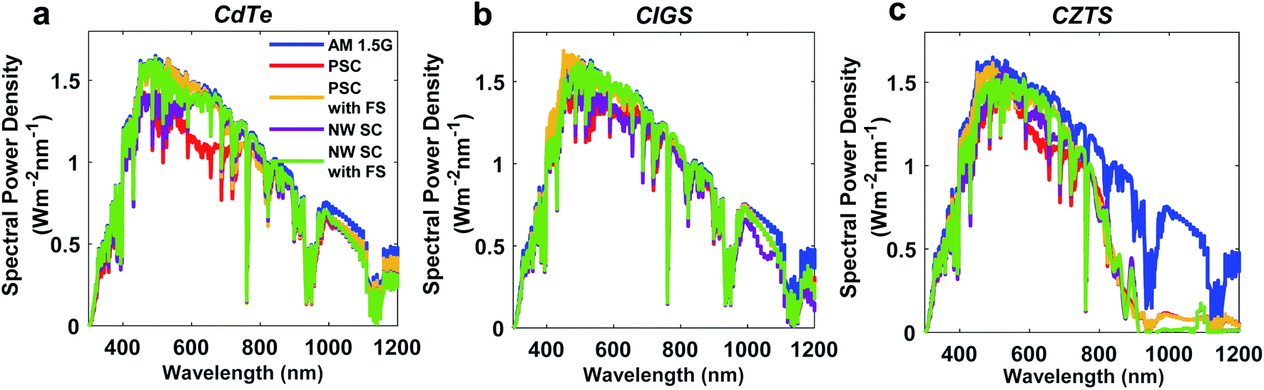
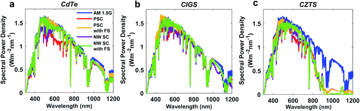
Fig. 7a–c show the absorbed power density at various wavelengths for the optimum cases, along with the standard AM 1.5G spectral power density for different absorber layers. For bare PSC, the CIGS absorber has the highest absorption for most of the wavelength range. The absorption in the CZTS absorber becomes insignificant beyond 800 nm, corresponding to the band edge. For CdTe solar cell, incorporating forward scatterer increases the absorption around 450–600 nm wavelength, whereas nanowire structure increases absorption in the 600–800 nm range. The combined effect is pronounced in forward scatterer incorporated NW SC giving improved absorption in the whole 450–800 nm visible wavelength region. Van Dam et al. showed that ITO hemispheres scatter most in the 400–700 nm wavelength range with peak scattering efficiency around 500 nm.36 Fig. 7a–c show that for all planar cells with forward scatterers, absorbed spectral power density is significantly improved in the 450–650 nm range. Hence our results conform with the predicted outcomes. For CIGS and CZTS, a similar trend is observed with absorption peak due to nanowires placed slightly right to that due to forward scatterers on PSCs. The difference between absorption spectra and AM 1.5G starts to get more pronounced beyond 1000 nm wavelength, where the extinction coefficients of these materials are extremely low.
 |
| | Fig. 7 Solar irradiance and absorbed power density for various (a) CdTe, (b) CIGS, and (c) CZTS solar cells (FS = Forward Scatterer). | |
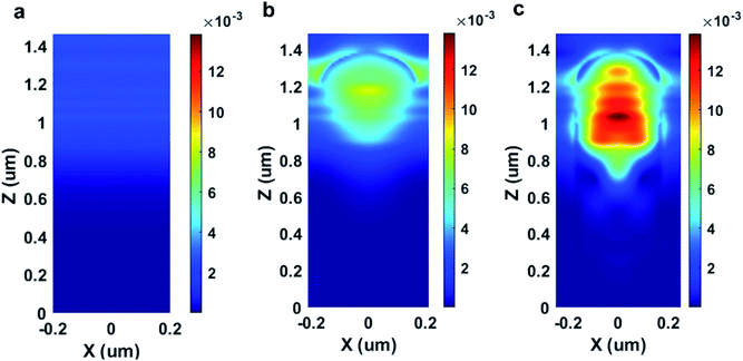
Fig. 8a–c, 9a–c, and 10a–c show the cross-sectional views of the electric field Poynting vector (W m−2) at 516 nm (optimum wavelength for absorption enhancement due to combined effects of nanowires and ITO hemispheres) wavelength for the different configurations of the three absorbers. The light concentration and field scattering effects are evident in these figures. For PSCs, light is concentrated below the center of the ITO hemispheres, along with the entrapment of scattered light between adjacent hemispheres (Fig. 8b, 9b, and 10b). For NW SC, both these effects persist (Fig. 8c, 9c, and 10c). However, the amount of light concentration around the center of the nanowire is higher due to the coupling of forward scattering and nanowire effects on light concentration. For NW SC, scattered light is also trapped in the space between adjacent nanowires, improving the light absorption around the edges of the nanowires. Hence, a much larger absorption cross-section is available for NW SCs, adding to its benefits.
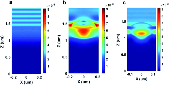 |
| | Fig. 8 Cross-sectional view of optical electric field power density (W m−2) at 516 nm wavelength for CdTe (a) bare PSC, (b) PSC with forward scatterer, and (c) NW SC with forward scatterer. | |
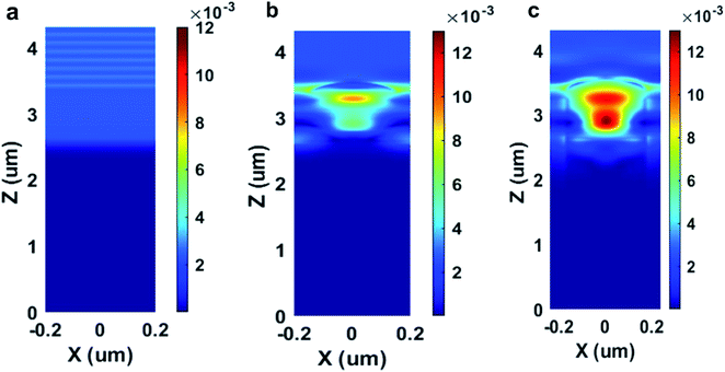 |
| | Fig. 9 Cross-sectional view of optical electric field power density (W m−2) at 516 nm wavelength for CIGS (a) bare PSC, (b) PSC with forward scatterer, and (c) NW SC with forward scatterer. | |
 |
| | Fig. 10 Cross-sectional view of optical electric field power density (W m−2) at 516 nm wavelength for CZTS (a) bare PSC, (b) PSC with forward scatterer, and (c) NW SC with forward scatterer. | |
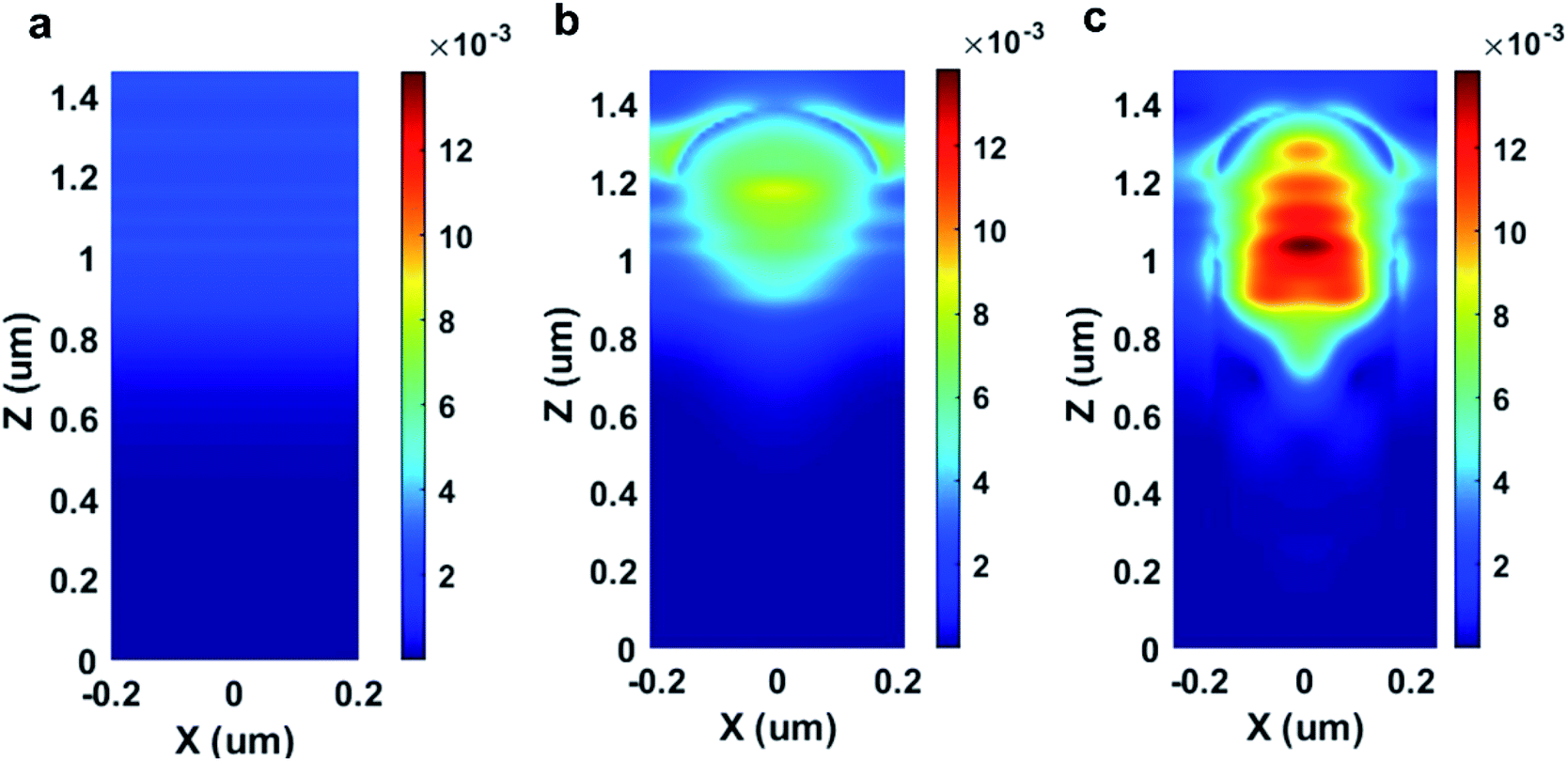
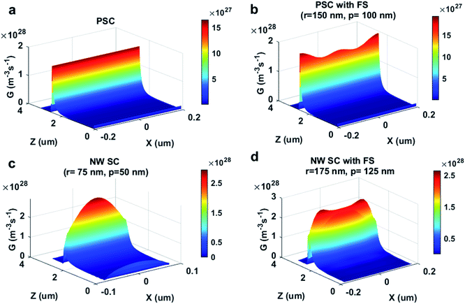
The enhanced electric field and light concentration get translated into an improved electron–hole-pair (EHP) generation rate (Fig. 11–13). The improvement can be observed through the maximum generation rate values. For CdTe, the highest EHP generation is below the center of the forward scattering hemisphere in planar cell (Fig. 11b) or at the center of NW SC (Fig. 11c and d). The improvement in absorption at the edges of the nanowires caused by light trapping is evident from Fig. 11c and d. When it comes to the CdTe absorber, the PSC with forward scatterer generates nearly twice as much EHP as the bare PSC, and both the bare and forward scatterer included NW SCs generate roughly three times as much EHP as the reference cell.
 |
| | Fig. 11 Cross-sectional views of EHP generation rate for CdTe (a) PSC, (b) PSC with forward scatterers, (c) bare NW SC, (d) NW SC with forward scatterers. For NW SCs, the cross-section goes through the center of the nanowire (FS = Forward Scatterer). | |
 |
| | Fig. 12 Cross-sectional view of EHP generation rate for CIGS (a) PSC, (b) PSC with forward scatterer, (c) bare NW SC, (d) NW SC with forward scatterer. For NW SCs, the cross-section goes through the center of the nanowire (FS = Forward Scatterer). | |
 |
| | Fig. 13 Cross-sectional view of EHP generation rate for CZTS (a) PSC, (b) PSC with forward scatterer, (c) bare NW SC, (d) NW SC with forward scatterer. For NW SCs, the cross-section goes through the center of the nanowire (FS = Forward Scatterer). | |
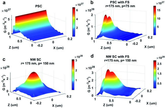
For CIGS absorber, bare PSC and PSC with forward scatterer show a similar range of generation rate, whereas NW SCs show 1.5-fold improvement in maximum generation rate than the planar cells (Fig. 12a–d). CIGS shows a higher generation below the edge of the hemispheres than their centers for both planar and NW SC (Fig. 12b and d). In the case of CZTS, a 5-fold improvement is found in the maximum generation rate for NW SC (Fig. 13c). The two peaks in generation rate of CZTS PSC with forward scatterer is due to the CdS absorber layer, which becomes significant for CZTS solar cell in the presence of forward scatterer (Fig. 13b). Thus, CZTS benefits the most in terms of maximum generation rate due to nanowire configuration (Fig. 13c) when compared to CdTe and CIGS, despite having the least enhancement in absorption (Fig. 5c).
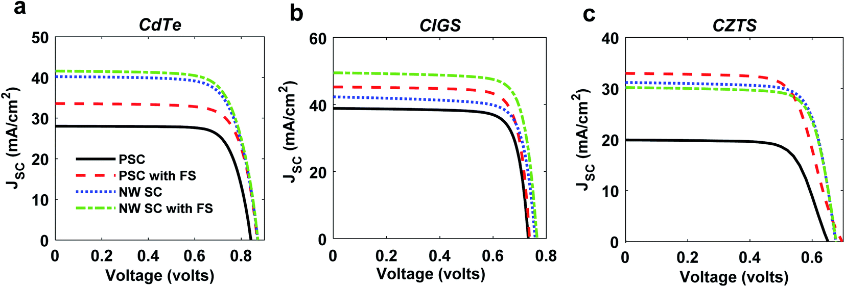
The generation rates were exported to COMSOL Multiphysics software to investigate the electrical properties of the solar cells. The obtained J–V characteristics are shown in Fig. 14a–c. Table 4 compares the improvement in PCEs for various cell types. For CdTe and CIGS solar cells, the maximum PCE is obtained for the case of NW SC with forward scatterer. For CdTe, the PCE enhances from 18.12% (Jsc = 28 mA cm−2) of reference cell to 26.45% (Jsc = 41.56 mA cm−2) for NW SC with forward scatterer, demonstrating a relative increase of 45.97%. In the case of CIGS, 32.05% improvement in PCE is observed as it increases from 22.5% to 29.7%, whereas Jsc increases from 38.85 mA cm−2 to 49.5 mA cm−2. However, for CZTS, the three cases exhibit similar improvement, with bare NW SC slightly leading with 87.94% PCE improvement (from 8.46% to 15.9%). Among the planar solar cells, the incorporation of forward scatterer benefits CZTS the most, with an 85.3% improvement in PCE. The CIGS absorber is least benefited from nanowire structure with only 9.91% improvement in PCE, yet this value may become significant considering material and cost reduction. These PCE enhancement values conform with the trend observed in maximum generation rate values of Fig. 11–13, where CZTS showed 5 times increase in maximum generation rate for bare NW SC (87.94% increase in PCE), while CdTe and CIGS showed 3 times and 1.5 times enhancement for NW SC with forward scatterer (45.97% and 32.09% increase in PCE, respectively). Thus, all the NW SCs show promising potential, which, coupled with the benefits of forward scatterers, greatly enhance their performance.
 |
| | Fig. 14 J–V and characteristics of (a) CdTe, (b) CIGS, and (c) CZTS solar cells (FS = Forward Scatterer). | |
Table 4 Comparison of improvement of electrical properties of various cells
| |
Parameters of interest |
Jsc (mA cm−2) |
Voc (volts) |
FF |
PCE (%) |
Improvement in PCE (%) |
| CdTe |
Planar solar cell |
28.00 |
0.84 |
0.77 |
18.12 |
— |
| Planar solar cell with forward scatterers |
33.59 |
0.869 |
0.755 |
22.04 |
21.63 |
| Nanowire solar cell |
40.20 |
0.87 |
0.73 |
25.57 |
41.11 |
| Nanowire solar cell with forward scatterers |
41.56 |
0.871 |
0.731 |
26.45 |
45.97 |
| CIGS |
Planar solar cell |
38.85 |
0.732 |
0.791 |
22.5 |
— |
| Planar solar cell with forward scatterers |
45.25 |
0.737 |
0.794 |
26.49 |
17.73 |
| Nanowire solar cell |
42.28 |
0.758 |
0.771 |
24.73 |
9.91 |
| Nanowire solar cell with forward scatterers |
49.5 |
0.765 |
0.784 |
29.72 |
32.09 |
| CZTS |
Planar solar cell |
19.93 |
0.651 |
0.652 |
8.46 |
— |
| Planar solar cell with forward scatterers |
32.98 |
0.698 |
0.681 |
15.68 |
85.3 |
| Nanowire solar cell |
31.18 |
0.676 |
0.754 |
15.90 |
87.94 |
| Nanowire solar cell with forward scatterers |
30.21 |
0.678 |
0.753 |
15.44 |
82.5 |
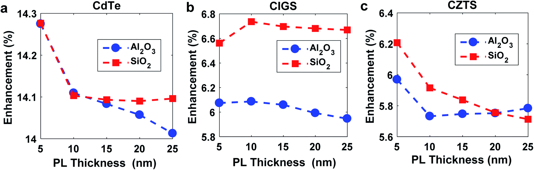
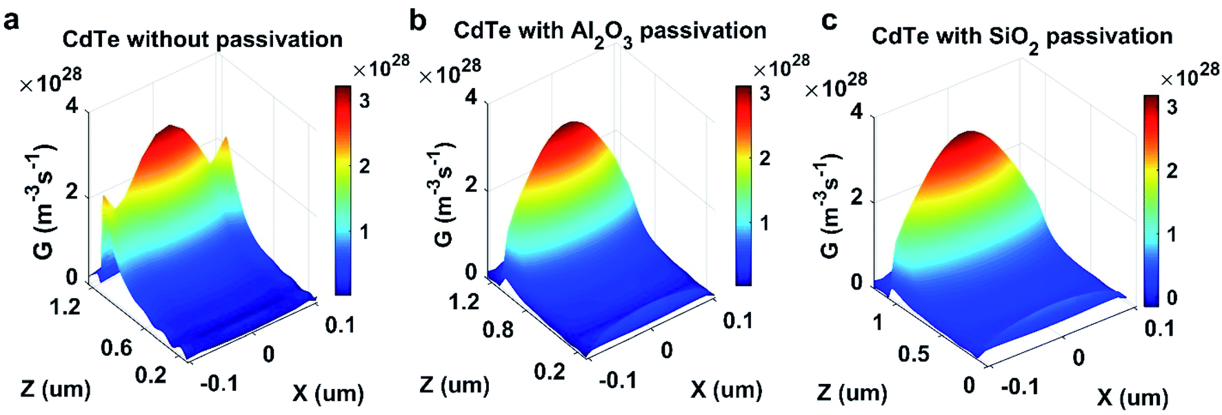
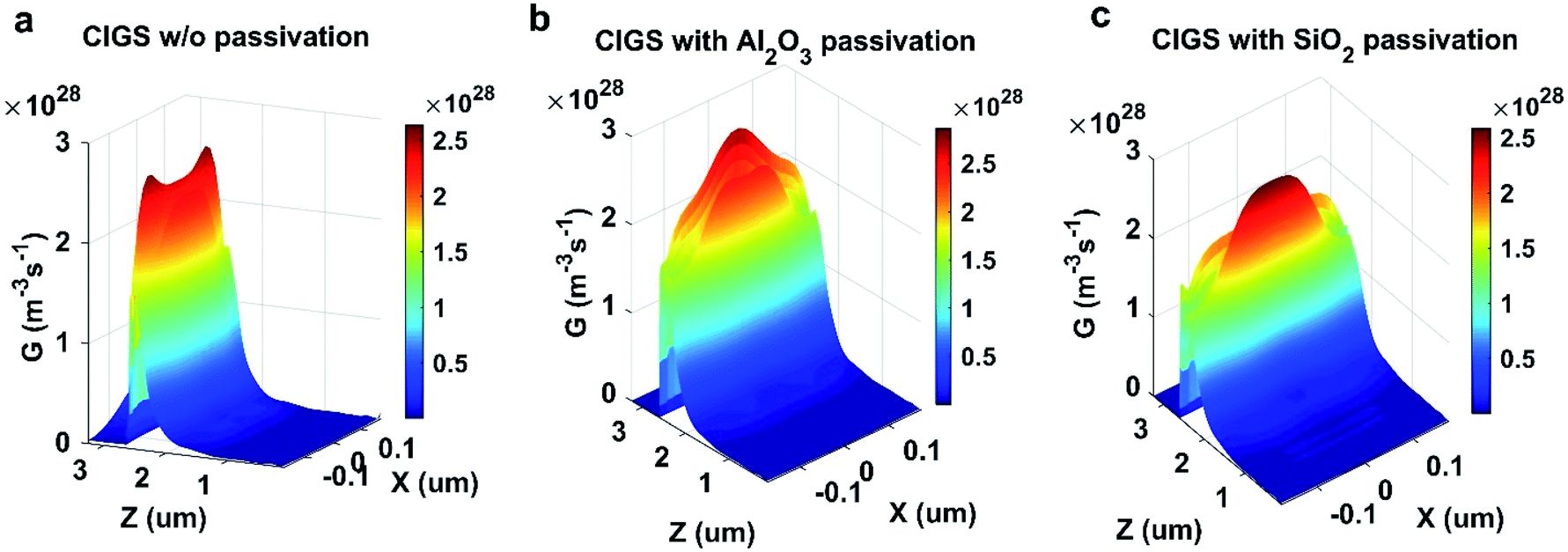
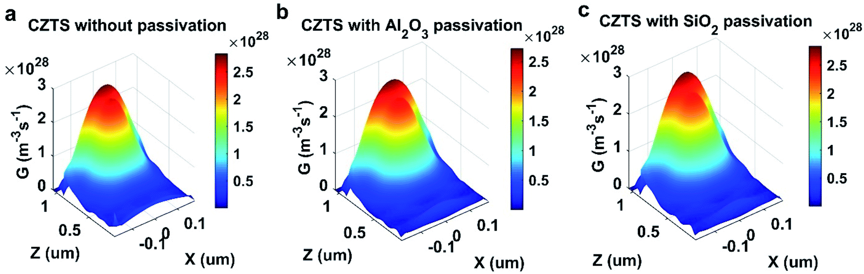
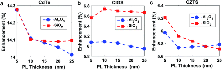
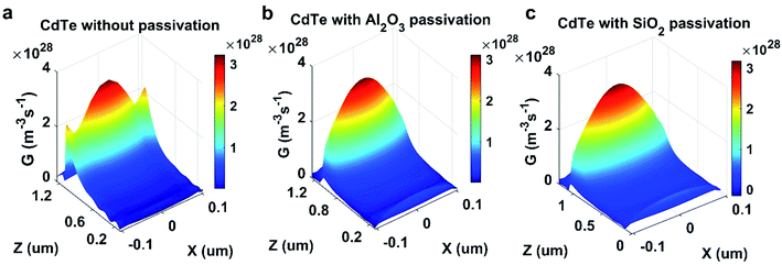
In order to study the effects of passivation on the NW SCs, Al2O3 and SiO2 PL surrounding the nanowires were added to previously optimized structures. The optical performance of the passivated cells were examined by varying the thickness of the PL from 5 nm to 25 nm, since most experimental studies have used a thickness of PL within this range. The enhancement in optical performance of these passivated cells compared to planar reference cells can be observed in Fig. 15. It is evident that both Al2O3 and SiO2 show very similar performance since the difference in their enhancement factor is negligible, with maximum difference of 0.6% obtained for CIGS solar cell. CdTe and CZTS cells show similar trend in enhancement factor variation with deteriorating enhancement at higher PL thickness and maximum enhancement at 5 nm PL. SiO2 as the PL shows slightly better performance in terms of optical characteristics in all three cases. This could be due to the fact that the relative permittivity of SiO2 (1.45704) at studied wavelengths is closer to that of the surrounding polymer (1.5). The maximum enhancement found after adding PL for CdTe and CIGS (14.28%, 6.9%) are lower than those of optimized structure for these two materials (21.4%, 7.36%), whereas maximum enhancement increases for CZTS at 5 nm thickness of PL (6.2% from 6.02%). The EHP generation rate profile for 10 nm PL can be observed in Fig. 16–18. The generation rate in CZTS after adding PL is negligibly altered (Fig. 18) validating the similar enhancement factors for optimized NW SC with and without PL (Fig. 15c). For CdTe and CIGS, the generation at the edges of nanowires diminish (Fig. 16 and 17), indicating that the scattering effect of nanowires has reduced.
 |
| | Fig. 15 Coupled absorption enhancement for Al2O3 and SiO2 passivated optimized (a) CdTe, (b) CIGS, and (c) CZTS nanowire solar cells with respect to corresponding reference cells. | |
 |
| | Fig. 16 Cross-sectional view of EHP generation rate for CdTe optimized FS incorporated NWSC with (a) no passivation (b) Al2O3 passivation (c) SiO2 passivation. | |
 |
| | Fig. 17 Cross-sectional view of EHP generation rate for CIGS optimized FS incorporated NWSC with (a) no passivation (b) Al2O3 passivation (c) SiO2 passivation. | |
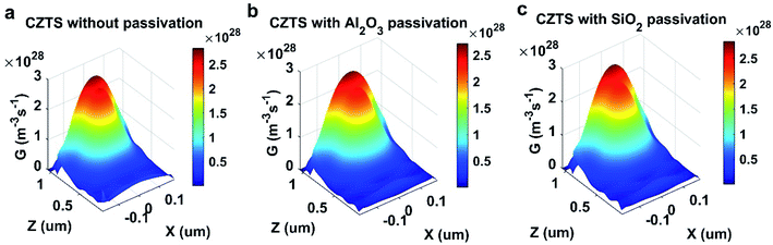 |
| | Fig. 18 Cross-sectional view of EHP generation rate for CZTS optimized FS incorporated NWSC with (a) no passivation (b) Al2O3 passivation (c) SiO2 passivation. | |
The generation rates from optical analyses were used to calculate the electrical parameters of passivated NW SC, which can be observed from Fig. 19. The layer thickness was chosen to be 10 nm since experimental studies have shown improved surface characteristics at this thickness. The J–V curves of CdTe and CZTS show a decrease in the Jsc value due to slightly reduced optical absorption. However, the Voc values for these materials remain unchanged after adding the PL, indicating that the reduction of surface recombination has resulted in the improvement of Voc despite lower current density. For CIGS, the effect of passivation is most prominent with SiO2 PL, enhancing the PCE from 29.72% for non-passivated cell to 32.47% for the passivated one (Table 5). The generation rate profiles of CIGS (Fig. 17a and b) demonstrated that addition of PL moves the location of peak EHP generation away from the CIGS/CdS interface. As a result, the number of charge carriers lost at this interface due to recombination at the surface defects is reduced. This coupled with lower recombination at passivated nanowire surface, results in the improvement of both Jsc and Voc, consequently improving the PCE (Table 5).
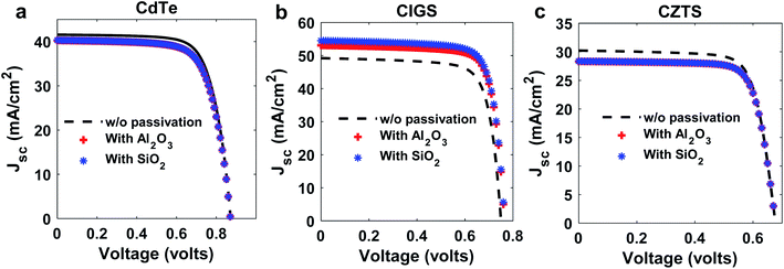 |
| | Fig. 19 J–V characteristics with and without PL for optimized (a) CdTe, (b) CIGS, and (c) CZTS NW SCs with FS. | |
Table 5 Effect of passivation layer on the electrical properties of optimized cells
| |
Parameters of interest |
Jsc (mA cm−2) |
Voc (volts) |
FF |
PCE (%) |
Improvement in PCE (%) |
| CdTe |
Optimized NW SC with FS |
41.56 |
0.871 |
0.731 |
26.45 |
45.97 |
| Optimized NW SC with FS and Al2O3 passivation |
40.26 |
0.871 |
0.717 |
25.13 |
38.69 |
| Optimized NW SC with FS and SiO2 passivation |
40.32 |
0.871 |
0.717 |
25.17 |
38.90 |
| CIGS |
Optimized NW SC with FS |
49.5 |
0.765 |
0.784 |
29.72 |
32.09 |
| Optimized NW SC with FS and Al2O3 passivation |
53.08 |
0.767 |
0.779 |
31.74 |
41.06 |
| Optimized NW SC with FS and SiO2 passivation |
54.52 |
0.768 |
0.775 |
32.47 |
44.31 |
| CZTS |
Optimized NW SC with FS |
30.21 |
0.678 |
0.753 |
15.44 |
82.5 |
| Optimized NW SC with FS and Al2O3 passivation |
28.32 |
0.678 |
0.767 |
14.73 |
74.09 |
| Optimized NW SC with FS and SiO2 passivation |
28.35 |
0.678 |
0.766 |
14.75 |
74.29 |
5. Conclusion
In summary, the performances of solar cells with three different absorber layers have been enhanced with two different mechanisms – using ITO hemispheres as forward scatterers and incorporating a nanowire-shaped absorber layer instead of the planar absorber. The optimum arrangement of ITO forward scatterers for improvement in optical absorption was consistent for all the absorbers with 150–175 nm radius and 75–100 nm pitch. However, the optimum dimension of nanowires varies significantly among the three absorber layers. The ultimate power conversion efficiency values predicted by our model are 26.45% and 29.72% for CdTe and CIGS NW SCs with forward scatterer, respectively. For CZTS, a maximum PCE of 15.9% was observed for bare NW SC, which used three times less material than the planar reference cell with 8.46% PCE. The significant reduction in material requirement coupled with increased efficiency can immensely impact the generation cost of solar power. The addition of passivation layer was found to be beneficial for the improvement of open-circuit voltage with a slight reduction in optical absorption and corresponding short-circuit current density. CIGS nanowire cell was most positively impacted by the addition of passivation layer with PCE improving to 32.47%. It is expected that this work will aid in the development of specific guidelines for the design of axial junction nanowire solar cells and help experimentalists comprehend the effects and potential of forward scatterers on the improvement of optical absorption in CdTe, CIGS, and CZTS axial junction nanowire solar cells.
Conflicts of interest
There are no conflicts to declare.
References
- M. A. Green, Prog. Photovoltaics, 2001, 9, 123–135 CAS.
- K. R. Catchpole and A. Polman, Appl. Phys. Lett., 2008, 93, 191113 CrossRef.
- K. Nakayama, K. Tanabe and H. A. Atwater, Appl. Phys. Lett., 2008, 93, 121904 CrossRef.
- D. M. Schaadt, B. Feng and E. T. Yu, Appl. Phys. Lett., 2005, 86, 1–3 CrossRef.
- S. A. Maier, in Plasmonics: Fundamentals and Applications, Springer US, New York, NY, 2007 Search PubMed.
- B. M. Kayes, H. A. Atwater and N. S. Lewis, J. Appl. Phys., 2005, 97, 114302 CrossRef.
- L. Tsakalakos, J. Balch, J. Fronheiser, B. A. Korevaar, O. Sulima and J. Rand, Appl. Phys. Lett., 2007, 91, 233117 CrossRef.
- E. Garnett and P. Yang, Nano Lett., 2010, 10, 1082–1087 CrossRef CAS PubMed.
- W. Wang, S. Wu, R. J. Knize, K. Reinhardt, Y. Lu, S. Chen, A. v Shah, H. Schade, M. Vanecek, J. Meier, E. Vallat-Sauvain, N. Wyrsch, U. Kroll, C. Droz and J. Bailat, Opt. Express, 2008, 20, 3733–3743 CrossRef PubMed.
- G. Otnes and M. T. Borgström, Nano Today, 2017, 12, 31–45 CrossRef CAS.
- P. Krogstrup, H. I. Jørgensen, M. Heiss, O. Demichel, J. v. Holm, M. Aagesen, J. Nygard and A. Fontcuberta I Morral, Nat. Photonics, 2013, 7, 306–310 CrossRef CAS.
- H. Lu and C. Gang, Nano Lett., 2007, 7, 3249–3252 CrossRef PubMed.
- J. M. Spurgeon, H. A. Atwater and N. S. Lewis, J. Phys. Chem. C, 2008, 112, 6186–6193 CrossRef CAS.
- L. Tsakalakos, J. Nanophotonics, 2007, 1, 013552 CrossRef.
- J. Zhu, Z. Yu, G. F. Burkhart, C. M. Hsu, S. T. Connor, Y. Xu, Q. Wang, M. McGehee, S. Fan and Y. Cui, Nano Lett., 2009, 9, 279–282 CrossRef CAS PubMed.
- N. Anttu and H. Q. Xu, Opt. Express, 2013, 21, A558 CrossRef CAS PubMed.
- V. T. Pham, M. Dutta, H. T. Bui and N. Fukata, Adv. Nat. Sci.: Nanosci. Nanotechnol., 2014, 5, 045014 CAS.
- Z. Fan, H. Razavi, J. W. Do, A. Moriwaki, O. Ergen, Y. L. Chueh, P. W. Leu, J. C. Ho, T. Takahashi, L. A. Reichertz, S. Neale, K. Yu, M. Wu, J. W. Ager and A. Javey, Nat. Mater., 2009, 8, 648–653 CrossRef CAS PubMed.
- G. Mariani, Z. Zhou, A. Scofield and D. L. Huffaker, Nano Lett., 2013, 13, 1632–1637 CrossRef CAS PubMed.
- K. Seo, M. Wober, P. Steinvurzel, E. Schonbrun, Y. Dan, T. Ellenbogen and K. B. Crozier, Nano Lett., 2011, 11, 1851–1856 CrossRef CAS PubMed.
- G. Brönstrup, C. Leiterer, N. Jahr, C. Gutsche, A. Lysov, I. Regolin, W. Prost, F. J. Tegude, W. Fritzsche and S. Christiansen, Nanotechnology, 2011, 22, 385201 CrossRef PubMed.
- L. Cao, J. S. White, J. S. Park, J. A. Schuller, B. M. Clemens and M. L. Brongersma, Nat. Mater., 2009, 8, 643–647 CrossRef CAS PubMed.
- O. L. Muskens, J. G. Rivas, R. E. Algra, E. P. A. M. Bakkers and A. Lagendijk, Nano Lett., 2008, 8, 2638–2642 CrossRef CAS PubMed.
- L. C. Chuang, M. Moewe, C. Chase, N. P. Kobayashi, C. Chang-Hasnain and S. Crankshaw, Appl. Phys. Lett., 2007, 90, 043115 CrossRef.
- T. Mårtensson, C. P. T. Svensson, B. A. Wacaser, M. W. Larsson, W. Seifert, K. Deppert, A. Gustafsson, L. R. Wallenberg and L. Samuelson, Nano Lett., 2004, 4, 1987–1990 CrossRef.
- T. J. Kempa, B. Tian, D. R. Kim, H. Jinsong, Z. Xiaolin and C. M. Lieber, Nano Lett., 2008, 8, 3456–3460 CrossRef CAS PubMed.
- E. Barrigón, L. Hrachowina and M. T. Borgström, Nano Energy, 2020, 78, 105191 CrossRef.
- M. Heurlin, M. H. Magnusson, D. Lindgren, M. Ek, L. R. Wallenberg, K. Deppert and L. Samuelson, Nature, 2012, 492, 90–94 CrossRef CAS PubMed.
- W. Metaferia, A. R. Persson, K. Mergenthaler, F. Yang, W. Zhang, A. Yartsev, R. Wallenberg, M.-E. Pistol, K. Deppert, L. Samuelson and M. H. Magnusson, Nano Lett., 2016, 16, 5701–5707 CrossRef CAS PubMed.
- R. Kapadia, Z. Fan and A. Javey, Appl. Phys. Lett., 2010, 96, 103116 CrossRef.
- S. A. Moiz, A. M. Nahhas, H. D. Um, S. W. Jee, H. K. Cho, S. W. Kim and J. H. Lee, Nanotechnology, 2012, 23, 145401 CrossRef PubMed.
- Y. Sun and J. A. Rogers, Semiconductor Nanomaterials for Flexible Technologies, William Andrew Publishing, Oxford, 1st edn, 2010, pp. 159–196 Search PubMed.
- P. Espinet-Gonzalez, I. Aberg, M. Borgstrom, L. Samuelson, H. A. Atwater, E. Barrigon, Y. Chen, G. Otnes, G. Vescovi, C. Mann, J. v. Lloyd, D. Walker and M. D. Kelzenberg, IEEE J. Photovoltaics, 2020, 10, 502–507 Search PubMed.
- V. Raj, K. Vora, L. Fu, H. H. Tan and C. Jagadish, ACS Nano, 2019, 13, 12015–12023 CrossRef CAS PubMed.
- E. C. Garnett and P. Yang, J. Am. Chem. Soc., 2008, 130, 9224–9225 CrossRef CAS PubMed.
- D. van Dam, N. J. J. van Hoof, Y. Cui, P. J. van Veldhoven, E. P. A. M. Bakkers, J. Gómez Rivas and J. E. M. Haverkort, ACS Nano, 2016, 10, 11414–11419 CrossRef CAS PubMed.
- I. Aberg, G. Vescovi, D. Asoli, U. Naseem, J. P. Gilboy, C. Sundvall, A. Dahlgren, K. E. Svensson, N. Anttu, M. T. Bjork and L. Samuelson, IEEE J. Photovoltaics, 2016, 6, 185–190 Search PubMed.
- S. Rühle, Sol. Energy, 2016, 130, 139–147 CrossRef.
- Z. Kordrostami and A. Yadollahi, Opt. Commun., 2020, 459, 125059 CrossRef CAS.
- T. D. Lee and A. U. Ebong, Renew. Sustain. Energy Rev., 2017, 70, 1286–1297 CrossRef CAS.
- M. Powalla, S. Paetel, E. Ahlswede, R. Wuerz, C. D. Wessendorf and T. Magorian Friedlmeier, Appl. Phys. Rev., 2018, 5, 041602 Search PubMed.
- M. Green, E. Dunlop, J. Hohl-Ebinger, M. Yoshita, N. Kopidakis and X. Hao, Prog. Photovoltaics Res. Appl., 2021, 29, 3–15 CrossRef.
- M. Nakamura, K. Yamaguchi, Y. Kimoto, Y. Yasaki, T. Kato and H. Sugimoto, IEEE J. Photovoltaics, 2019, 9, 1863–1867 Search PubMed.
- C. Yan, J. Huang, K. Sun, S. Johnston, Y. Zhang, H. Sun, A. Pu, M. He, F. Liu, K. Eder, L. Yang, J. M. Cairney, N. J. Ekins-Daukes, Z. Hameiri, J. A. Stride, S. Chen, M. A. Green and X. Hao, Nat. Energy, 2018, 3(9), 764–772 CrossRef CAS.
- Y. Kang, N. G. Park and D. Kim, Appl. Phys. Lett., 2005, 86, 1–3 Search PubMed.
- R. Salazar, A. Delamoreanu, C. L. Clément and V. Ivanova, Energy Proc., 2011, 10, 122–127 CrossRef CAS.
- M. Zhang, Y. N. Wang, E. Moulin, D. Grützmacher, C. J. Chien, P. C. Chang, X. Gao, R. Carius and J. G. Lu, J. Mater. Chem., 2012, 22, 10441–10443 RSC.
- A. Melliti, Opt. Quant. Electron., 20121, 53, 91 CrossRef.
- T. J. Hsueh, J. M. Shieh and Y. M. Yeh, Prog. Photovoltaics Res. Appl., 2015, 23, 507–512 CrossRef CAS.
- R. Cohen, V. Lyahovitskaya, E. Poles, A. Liu and Y. Rosenwaks, Appl. Phys. Lett., 1998, 73, 1400–1402 CrossRef CAS.
- P. M. P. Salomé, B. Vermang, R. Ribeiro-Andrade, J. P. Teixeira, J. M. v. Cunha, M. J. Mendes, S. Haque, J. Borme, H. Águas, E. Fortunato, R. Martins, J. C. González, J. P. Leitão, P. A. Fernandes, M. Edoff and S. Sadewasser, Adv. Mater. Interfaces, 2018, 5, 1701101 CrossRef.
- M. O. Reese, C. L. Perkins, J. M. Burst, S. Farrell, T. M. Barnes, S. W. Johnston, D. Kuciauskas, T. A. Gessert and W. K. Metzger, J. Appl. Phys., 2005, 118, 155305 CrossRef.
- J. M. Kephart, A. Kindvall, D. Williams, D. Kuciauskas, P. Dippo, A. Munshi and W. S. Sampath, IEEE J. Photovoltaics, 2018, 8, 587–593 Search PubMed.
- H. Li, J. Chen, Y. Zhang, W. Wang and H. Gu, ACS Appl. Energy Mater., 2020, 3, 9459–9467 CrossRef CAS.
- E. Ojeda-Durán, K. Monfil-Leyva, J. Andrade-Arvizu, I. Becerril-Romero, Y. Sánchez, R. Fonoll-Rubio, M. Guc, Z. Jehl, J. A. Luna-López, A. L. Muñoz-Zurita, J. A. D. Hernández-de la Luz, V. Izquierdo-Roca, M. Placidi and E. Saucedo, Sol. Energy, 2020, 198, 696–703 CrossRef.
- J. M. Burst, J. N. Duenow, D. S. Albin, E. Colegrove, M. O. Reese, J. A. Aguiar, C. S. Jiang, M. K. Patel, M. M. Al-Jassim, D. Kuciauskas, S. Swain, T. Ablekim, K. G. Lynn and W. K. Metzger, Nat. Energy, 2016, 1, 16015 CrossRef CAS.
- N. M. Martin, C. Platzer-Björkman, K. Simonov, H. Rensmo and T. Törndahl, Phys. Status Solidi B, 2020, 257, 2000308 CrossRef CAS.
- J. Park, J. Huang, J. Yun, F. Liu, Z. Ouyang, H. Sun, C. Yan, K. Sun, K. Kim, J. Seidel, S. Chen, M. A. Green and X. Hao, Adv. Energy Mater., 2018, 8, 1701940 CrossRef.
- Y. S. Lee, T. Gershon, T. K. Todorov, W. Wang, M. T. Winkler, M. Hopstaken, O. Gunawan and J. Kim, Adv. Energy Mater., 2016, 6, 1600198 CrossRef.
- D. G. Buldu, J. de Wild, T. Kohl, G. Birant, G. Brammertz, M. Meuris, J. Poortmans and B. Vermang, IEEE J. Photovoltaics, 2022, 12, 301–308 Search PubMed.
- F. K. Alfadhili, A. B. Phillips, K. K. Subedi, C. L. Perkins, A. I. Halaoui, M. K. Jamarkattel, B. M. Anwar, G. K. Liyanage, D. B. Li, C. R. Grice, Y. Yan, R. J. Ellingson and M. J. Heben, ACS Appl. Mater. Interfaces, 2020, 12, 51337–51343 CrossRef CAS PubMed.
- M. A. Curado, J. P. Teixeira, M. Monteiro, E. F. M. Ribeiro, R. C. Vilão, H. v. Alberto, J. M. V. Cunha, T. S. Lopes, K. Oliveira, O. Donzel-Gargand, A. Hultqvist, S. Calderon, M. A. Barreiros, W. Chiappim, J. P. Leitão, A. G. Silva, T. Prokscha, C. Vinhais, P. A. Fernandes and P. M. P. Salomé, Appl. Mater. Today, 2020, 21, 100867 CrossRef.
- G. Zeng, X. Hao, S. Ren, L. Feng and Q. Wang, Energies, 2019, 12, 1123 CrossRef CAS.
- K. Oliveira, J. P. Teixeira, W. C. Chen, J. Lontchi Jioleo, A. J. N. Oliveira, I. Caha, L. D. Francis, D. Flandre, M. Edoff, P. A. Fernandes and P. M. P. Salome, IEEE J. Photovoltaics, 2022, 12, 954–961 Search PubMed.
- T. Pu, H. Shen and Q. Tang, Silicon, 2022, 14, 3339–3348 CrossRef CAS.
- V. Budhraja, Int. J. Eng. Res., 2015, 4, 10–12 Search PubMed.
- J. E. M. Haverkort, E. C. Garnett and E. P. A. M. Bakkers, Appl. Phys. Rev., 2018, 5, 031106 Search PubMed.
- A. Acevedo-Luna, R. Bernal-Correa, J. Montes-Monsalve and A. Morales-Aceved, J. Appl. Res. Technol., 2017, 15, 599–608 CrossRef.
- E. Akbarnejad, Z. Ghorannevis, E. Mohammadi and L. Fekriaval, J. Electroanal. Chem., 2019, 849, 113358 CrossRef CAS.
- M. W. Bouabdelli, F. Rogti, M. Maache and A. Rabehi, Optik, 2020, 216, 164948 CrossRef CAS.
- A. Kumar, A. Kumar Goyal, U. Gupta, Tanya, N. Gupta and R. Chaujar, Mater. Today: Proc., 2020, 28, 361–365 CAS.
- T. Nakada, Y. Hirabayashi, T. Tokado, D. Ohmori and T. Mise, Sol. Energy, 2004, 77, 739–747 CrossRef CAS.
- R. Bernal-Correa, A. Morales-Acevedo and J. Montes-Monsalve, in International Conference on Electrical Engineering, Computing Science and Automatic Control (CCE), 2018, pp. 1–7 Search PubMed.
- J. K. Sim, D. Y. Um, J. W. Kim, J. S. Kim, K. U. Jeong and C. R. Lee, J. Alloys Compd., 2019, 779, 643–647 CrossRef CAS.
- G. Mariani, P.-S. Wong, A. M. Katzenmeyer, F. Léonard, J. Shapiro and D. L. Huffaker, Nano Lett., 2011, 11, 2490–2494 CrossRef CAS PubMed.
- Comsol Multiphysics 5.4, Comsol Inc., 2018 Search PubMed.
- J. M. V. Cunha, K. Oliveira, J. Lontchi, T. S. Lopes, M. A. Curado, J. R. S. Barbosa, C. Vinhais, W. C. Chen, J. Borme, H. Fonseca, J. Gaspar, D. Flandre, M. Edoff, A. G. Silva, J. P. Teixeira, P. A. Fernandes and P. M. P. Salomé, Sol. RRL, 2021, 5, 2000534 CrossRef CAS.
- M. Gloeckler, I. Sankin and Z. Zhao, IEEE J. Photovoltaics, 2013, 3, 1389–1393 Search PubMed.
- F. Liu, J. Huang, K. Sun, C. Yan, Y. Shen, J. Park, A. Pu, F. Zhou, X. Liu, J. A. Stride, M. A. Green and X. Hao, NPG Asia Mater., 2017, 9, 401 CrossRef.
- M. Burgelman, P. Nollet and S. Degrave, Appl. Phys. A, 1999, 69, 149–153 CrossRef CAS.
- A. Kanevce and T. A. Gessert, IEEE J. Photovoltaics, 2011, 1, 99–103 Search PubMed.
- J. Sites and J. Pan, Thin Solid Films, 2007, 515, 6099–6102 CrossRef CAS.
- Md. Asaduzzaman, M. Hasan and A. N. Bahar, SpringerPlus, 2016, 5, 1–8 CrossRef CAS PubMed.
- M. A. Halim, M. M. Islam, X. Luo, T. Sakurai, N. Sakai, T. Kato, H. Sugimoto, H. Tampo, H. Shibata, S. Niki and K. Akimoto, AIP Adv., 2016, 6, 035216 CrossRef.
- M. Mostefaoui, H. Mazari, S. Khelifi, A. Bouraiou and R. Dabou, Energy Proc., 2015, 74, 736–744 CrossRef CAS.
- T. P. Weiss, R. Carron, M. H. Wolter, J. Löckinger, E. Avancini, S. Siebentritt, S. Buecheler and A. N. Tiwari, Sci. Technol. Adv. Mater., 2019, 20, 313–323 CrossRef CAS PubMed.
- F. Werner, B. Veith-Wolf, M. Melchiorre, F. Babbe, J. Schmidt and S. Siebentritt, Sci. Rep., 2020, 10, 1–14 CrossRef PubMed.
- M. Jiang and X. Yan, Solar Cells – Research and Application Perspectives, InTech, Croatia, 2013 Search PubMed.
- U. Saha and Md. K. Alam, RSC Adv., 2017, 7, 4806–4814 RSC.
- W. Martienssen and H. Warlimont, Handbook of condensed matter and materials
data, Springer Science & Business Media, Berlin, 2005 Search PubMed.
- R. L. Williams, Can. J. Phys., 1958, 36, 1536–1550 CrossRef CAS.
- B. Hussain, A. Aslam, T. M. Khan, M. Creighton and B. Zohuri, Electronics, 2019, 8, 238 CrossRef CAS.
- A. Janotti and C. G. van de Walle, Reports on Progress in Physics, IOP Publishing Ltd, Brostol, United Kingdom, 2009, vol. 72, p. 126501 Search PubMed.
- O. Madelung, Semiconductors: Data Handbook, Springer, Berlin, 2004 Search PubMed.
- A. Benmir and M. S. Aida, Energy Proc., 2013, 36, 618–627 CrossRef CAS.
- R. Carron, E. Avancini, T. Feurer, B. Bissig, P. A. Losio, R. Figi, C. Schreiner, M. Bürki, E. Bourgeois, Z. Remes, M. Nesladek, S. Buecheler and A. N. Tiwari, Sci. Technol. Adv. Mater., 2018, 19, 396 CrossRef CAS PubMed.
- C. H. Swartz, M. Edirisooriya, E. G. LeBlanc, O. C. Noriega, P. A. R. D. Jayathilaka, O. S. Ogedengbe, B. L. Hancock, M. Holtz, T. H. Myers and K. N. Zaunbrecher, Appl. Phys. Lett., 2014, 105, 222107 CrossRef.
- X. Fan, W. Zheng and D. J. Singh, Light: Sci. Appl., 2014, 3, e179 CrossRef CAS.
Footnote |
| † Present Address: Department of Electrical Engineering, Stanford University, Stanford, California 94305, USA. |
|
| This journal is © The Royal Society of Chemistry 2022 |
Click here to see how this site uses Cookies. View our privacy policy here. 
 Open Access Article
 This Open Access Article is licensed under a Creative Commons Attribution-Non Commercial 3.0 Unported Licence
 *
*