
 Open Access Article
 This Open Access Article is licensed under a Creative Commons Attribution-Non Commercial 3.0 Unported Licence
Improved phase purity and film quality in quasi-2D perovskite light-emitting diodes by an additive with the trimethacrylate group†
Xiaofeng Huangab,
Wu Liuab,
Wei Wangab,
Yao Luab,
Jie Dong ab,
Yueqiao Liab,
Dong Weic,
Bo Qiaoab,
Suling Zhaoab,
Zheng Xuab and
Dandan Song*ab
ab,
Yueqiao Liab,
Dong Weic,
Bo Qiaoab,
Suling Zhaoab,
Zheng Xuab and
Dandan Song*ab
aKey Laboratory of Luminescence and Optical Information, Beijing Jiaotong University, Ministry of Education, Beijing 100044, China. E-mail: ddsong@bjtu.edu.cn
bInstitute of Optoelectronics Technology, Beijing Jiaotong University, Beijing 100044, China
cCollege of Physics and Energy, Fujian Normal University, Fuzhou, 350117, China
First published on 24th January 2022
Abstract
Quasi-2D perovskites are potential materials for optoelectronics like light-emitting diodes (LEDs); compared to their 3D counterparts, they are considered more stable against the atmosphere and more efficient in exciton confining. However, the simultaneous formation of different phases in the quasi-2D perovskite film, i.e., the phase impurity issue, lowers the device performance. We propose using a small molecule additive, trimethylolpropane trimethacrylate (TMPTA), to suppress the phase impurity by mixing it into the antisolvent. The phase pure quasi-2D perovskite film was obtained, and meanwhile, the film quality was also improved. Moreover, the ester functional groups in TMPTA also passivate the charged defects in the perovskite film, minimizing the carrier recombination in the device. Correspondingly, with TMPTA modification, the maximum current efficiency is increased by 25%, and the half lifetime of the PeLEDs is prolonged by three times.
1. Introduction
As a new generation of optoelectronic materials, perovskites have advantages including efficient carrier transportability, adjustable exciton binding energy, and low trap state density.1–4 Hence, they have been widely used in light-emitting diodes (LEDs),5 solar cells,6 photodetectors,7 lasers,8 etc. The chemical formula of three-dimensional (3D) perovskite materials is ABX3, where A is a monovalent cation, B is a divalent metal cation (typically Pb2+or Sn2+), and X is a halogen ion (I−, Br−, Cl−). By inserting large aliphatic or aromatic organic ammonium cations A′(n-butylammonium BA+ and phenylethylammonium PEA+, etc.) into 3D perovskites, quasi-2D perovskites can be formed, with the chemical formula of An−1BnX3n+1, compared with 3D perovskite, quasi-2D perovskites have superior performance due to the quantum confinement effect and dielectric confinement effect.9–11
In recent years, high-performance quasi-2D perovskite LEDs (PeLEDs) have been achieved through a variety of strategies, including additive engineering,12 solvent engineering,13 interface modification,14 chemometric engineering,15 solvent vapor assisted crystallization,16 etc., and these methods help to improve the perovskite morphology and passivate defects. For example, You et al. inserted the organic molecule trioctyl phosphine oxide (TOPO) on top of the quasi-2D perovskite layer. Thus, the unbonded lead is passivated through coordinating the P![[double bond, length as m-dash]](https://www.rsc.org/images/entities/char_e001.gif) O functional group in TOPO.17 As a result, the device external quantum efficiency (EQE) reached 14.36%.
O functional group in TOPO.17 As a result, the device external quantum efficiency (EQE) reached 14.36%.
Nonetheless, quasi-2D PeLEDs still face severe challenges due to the mediocre film quality and the quasi-2D perovskite emission layer (EML) phase impurity. Due to the reduced grain size and the thin thickness of quasi-2D perovskite film, defects tend to form at the grain boundaries and interfaces;18,19 meanwhile, small pinholes may be formed and lead to the current leakage from the EML.20 Moreover, the quasi-2D perovskite film typically suffers from phase impurity, i.e., many unexpected phases formed simultaneously with the expected phase. For instance, for the precursor solution to make  An−1BnX3n+1 (n = 4 or 5) phase, both larger n (n = 6, …, ∞) and smaller n (n = 2, 3) phases are formed in the film. Different phases have different optical and electrical properties, and the distribution and arrangement of layer impurities have an essential impact on the film's performance.21 On one hand, these unexpected phases may induce carrier trapping and/or increase sheet resistance due to the different energy levels of different n phases. On the other, the EQE may also be reduced as the exciton binding energy, and the photoluminescence quantum yield (PLQY) of the large n phases are low.22 The formation of different n phases from the stoichiometric ratio is probably due to the different solubilities of A′ and A cations, making their consumption rates different during the crystallization process, leading to the formation of different n phases. In addition, since the formation energies of different n phases are also different,23 this also promotes the formation of different n phases. Approaches on minimizing the phase purity are less learnt compared to other aspects like the film quality control. Present attempts show that the following methods are probably efficient: (1) adjusting the organic spacer cations to affect the formation of phase impurities by changing the crystallization process, interlayer interaction and formation energy of the quasi-2D dimensional perovskite film;24 (2) using additives to reduce phase impurities by interacting with ions in the solution to slow down crystal growth,25,26 thereby controlling the nucleation and minimizing phase segregation.
Here, we use a new type of insulating organic small molecule additive, trimethylolpropane trimethacrylate (TMPTA), to modify the quasi-2D perovskite layer. TMPTA was dissolved in ethyl acetate antisolvent to minimize phase impurities and improve the film quality of the quasi-2D perovskite film. TMPTA contains a ternary CO functional group, which can coordinate with the ions in the precursor solution to modify the crystallization process; moreover, these functional groups can also passivate the defects in the perovskite EML. Compared with the control device, the improved device shows better performance with the maximum luminance of 14![[thin space (1/6-em)]](https://www.rsc.org/images/entities/char_2009.gif) 790 cd m−2 and the maximum current efficiency of 22.3 cd A−1.
790 cd m−2 and the maximum current efficiency of 22.3 cd A−1.
2. Experimental section
2.1. Materials
Trimethylolpropane trimethacrylate (TMPTA, stabilized with MEHQ) was purchased from Innochem. PbBr2, CsBr, FABr, GABr, ethyl acetate (EA), chlorobenzene (CB) and 2,2′,2′′-(1,3,5-benzinetriyl)-tris(1-phenyl-1-H-benzimidazole) (TPBi) were purchased from Xi'an Polymer Light Technology Corp. PEABr was purchased from Dyesol. PEDOT:PSS (Clevious P VP Al 4083) was fabricated by Heraeus. Dimethyl sulfoxide (DMSO) was purchased from Alfa Aesar.2.2. Device fabrication
The perovskite precursor solution was prepared by mixing PbBr2:FABr:CsBr:GABr:PEABr = 1:0.7:0.25:0.05:0.4 in DMSO with stirring. TMPTA was dissolved in the antisolvent with a 0.25% and 0.5% volume ratio, respectively. First, m-PEDOT:PSS (PEDOT:PSS doped with PSS–Na) layer was spin-coated on the pre-cleaned ITO (135 nm) coated glass substrate at 3000 rpm for 40 s, and annealed at 150° for 15 minutes. Then they were quickly transferred to a nitrogen-filled glove box. The perovskite precursor solution was dynamically spin-coated at 4000 rpm for 60 seconds, and at 20th second, 100 μL of antisolvent was added dropwise. Then the samples were annealed at 70° for 10 minutes to obtain quasi-2D perovskite film. Finally, the samples were transferred to a vacuum thermal evaporation system to deposit TPBi (30 nm), LiF (0.8 nm), and Al (100 nm) layers in sequence at a pressure of 5 × 10⁻⁴ Pa. All measurements were carried out in ambient conditions at room temperature without encapsulation unless otherwise specified. The active area of the PeLEDs, depending on the deposition mask, is 9 mm2.
2.3. Characterization
The current density–voltage–luminance characteristics, the external quantum efficiency data and the electroluminescence spectra were recorded by a Newport 1830-R optical power meters equipped with 918D calibrated photodiode and Keithley 2400 Source Meter. Scanning electron microscope measurements were performed by a Hitachi 4800. The atomic force microscope images of the perovskite films were obtained using a Bruker atomic force microscope. X-ray diffraction patterns were collected with a D/max 2200 V X-ray powder diffractometer with Cu-Kα radiation. The absorption spectra were measured using an ultraviolet-visible spectrophotometer (UV-3101PC). The steady-state photoluminescence spectra were recorded on a Hitachi F4500 fluorescence spectrophotometer with a Xe lamp coupled to a monochromator. Time-resolved photoluminescence was achieved through the TBX picosecond photon detection module and single-photon counting controller Fluoro Hub. X-ray photoelectron spectrometer was obtained by routine measurement (ESCALAB 250Xi, Thermo Fisher Scientific). The AC impedance spectrum of the device was obtained by electrochemical workstation (Zahner, Germany) under no light conditions, and the frequency range was 100 kHz to 100 MHz.3. Results and discussion
The device structure of the PeLEDs is ITO/m-PEDOT:PSS/quasi-2D perovskite EML/TPBi/LiF/Al, as shown in Fig. 1a. Here, m-PEDOT:PSS is used as the hole transport layer (HTL) and TPBi as the electron transport layer (ETL); quasi-2D perovskite film was fabricated either without or with TMPTA modified ethyl acetate (EA) antisolvent, and is used as emission layer (EML). The corresponding energy level diagram is shown in Fig. 1b. From Fig. 1b, it can be seen that the different n phases have different energy levels, which will affect the device performance through modifying the carrier transport and recombination processes. The cross-sectional scanning electron microscope (SEM) image of the device is shown in Fig. 1c. The molecular structure of TMPTA is shown in Fig. 1d. It has 6 hydrogen bond acceptors and ternary ester functional groups, which benefit for passivating the charged defects in the film. In addition, it can also affect the crystallization process by interacting with the ions in the fabrication process. It has a value of 3.8 for XLogP3,27 which means that it is facile to be dissolved in lipophilic solvents while it is difficult in hydrophilic solvents. Hence, it was dissolved in the EA antisolvent to modify the perovskite EML. | ||
| Fig. 1 (a and b) Schematic device structure (a) and energy level diagram (b) of quasi-2D PeLEDs. (c) Cross-sectional SEM image of the device. (d) Molecular structure of TMPTA. | ||
The electroluminescence (EL) performance of the PeLEDs without or with TMPTA modification is shown in Fig. 2a and b. The exact values of the EL parameters are listed in Table 1. The results show that when the proportion of additive in the antisolvent is 0.25%, the overall device performance is optimal. The optimal device shows a maximum luminance (Lmax) of 14790 cd m−2, a maximum current efficiency (CEmax) of 22.3 cd A−1, and a maximum external quantum efficiency (EQE) of 6.05%. From Fig. 2a, it can also be seen that when the additive ratio in antisolvent is 0.25%, both the current density and the luminance at low voltages are increased, probably due to the improved film conductivity by TMPTA modification. Simultaneously, the turn-on voltage of the corresponding device is lowered. However, as TMPTA has poor conductivity, which inhibits carrier transport at a high concentration of 0.5%, the corresponding device shows low current density. Hence, the increased current density at 0.25% TMPTA condition can be ascribed to its modification on the perovskite layer other than the carrier transportability of TMPTA. The change on the perovskite layer probably correlates with defect passivation and/or improved film quality, which will be explored later. It shall be noted that all the L–V curves descend at high voltages, which can be ascribed to the reduced radiative efficiency at high temperatures induced by Joule heating at high current densities. The 0.25% TMPTA modification device has the largest current density at a specific voltage, so the luminance decreases more seriously at high voltages. This is a problem that needs to be solved in the future. The normalized EL spectra of the PeLEDs under 4.8 V are shown in Fig. 2c. There is a slight blue shift in the peak wavelength (λEL) with increasing TMPTA concentration. This is a typical signal for the defect passivation of the perovskite film.28,29
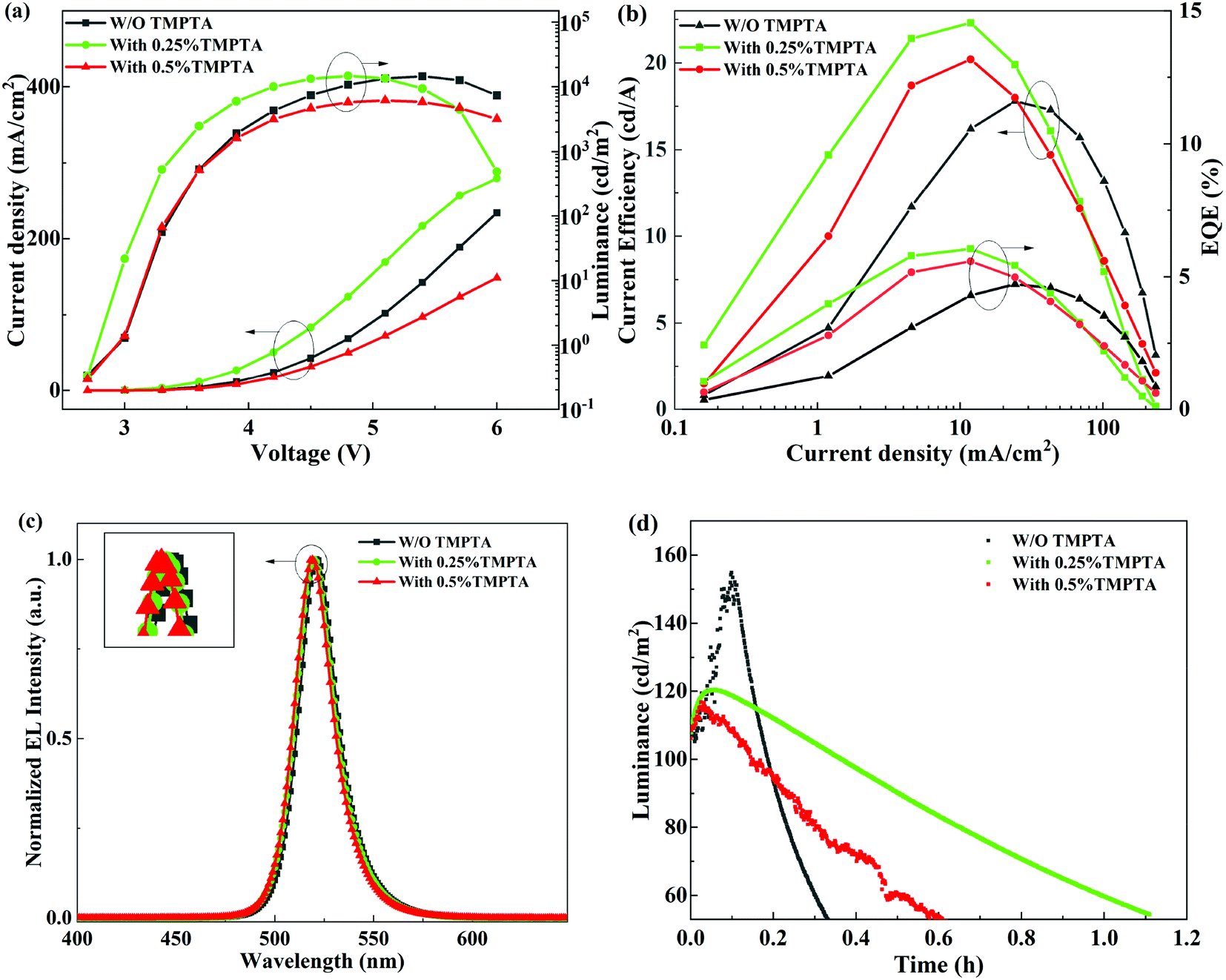 | ||
| Fig. 2 (a) Current density–voltage–luminance (J–V–L) curves, (b) current efficiency and external quantum efficiency versus current density (CE–J and EQE–J) curves, (c) normalized EL spectra, and (d) device degradation profiles aged under a constant current enabling an initial luminance of 100 cd m−2 of the PeLEDs without and with TMPTA modification. The ratio of TMPTA is its concentration in antisolvent. | ||
| Device | Von (V) | Lmax (cd m−2) | CEmax (cd A−1) | EQE (%) | FWHM (nm) | λEL (nm) |
|---|---|---|---|---|---|---|
| Control | 2.9 | 14607 |
17.8 | 4.72 | 23 | 521 |
| 0.25% TMPTA | 2.8 | 14790 |
22.3 | 6.05 | 22 | 520 |
| 0.5% TMPTA | 2.9 | 6214 | 20.2 | 5.58 | 22 | 519 |
Apart from the improved device EL performance, the device stability is also improved by TMPTA modification. As shown in Fig. 2d, the device luminance first increases with the degradation time at a constant current density enabling the initial luminance of 100 cd m−2, and then decreases. The increase in the luminance at the initial degradation stage can be ascribed to the defect healing effect in many kinds of LEDs. The device degradation induces a subsequent decrease in luminance. The half lifetime at which the luminance decreases to half of the initial value is increased obviously, which is nearly three times higher from the device modified with 0.25% TMPTA than from the standard device without modification. The long duration of the PeLEDs with TMPTA modification, especially at 0.25% TMPTA, reveals that the device stability is greatly improved. It is not mainly caused by the hydrophobicity of TMPTA, as the device stability of the PeLEDs modified with more TMPTA (0.5%) is inferior to that with less TMPTA (0.25%). The improved device stability by TMPTA modification can result from the reduced defects and/or the enhanced film quality that minimizes the film degradation of perovskite, and/or the modified interfaces that minimize interface degradation.
In order to have a deep understanding of the internal mechanism of TMPTA on the improvement of device EL performance and stability, the morphology of the perovskite film was firstly characterized by scanning electron microscope (SEM) and atomic force microscope (AFM). As shown in Fig. 3a–c, it can be seen that the quasi-2D perovskite film without TMPTA modification is not dense and uniform, and there is obvious unevenness on the surface. This may be because the crystal growth with the assistance of the antisolvent is too fast to cause continuous and uniform growth, so the unevenness and defects can be formed on the surface of the perovskite. With 0.25% TMPTA modification, the perovskite film grows densely and uniformly, and the grain size is also decreased small. AFM images shown in Fig. 3d–f also reveal the reduced surface roughness by TMPTA modification, which shows that the mean roughness (Ra) is reduced from 0.413 nm from the standard film without change to 0.115 nm from the film with 0.25% TMPTA modification. These modifications in the perovskite film benefit for better EL performance through enhancing carrier transport, reducing current leakage and enlarging exciton confinement. As the ester functional groups contained in TMPTA can form chemical bonds with the ions like Pb2+ in the perovskite precursor, which limits the crystallization speed of the perovskite, probably responsible for the improved film quality.
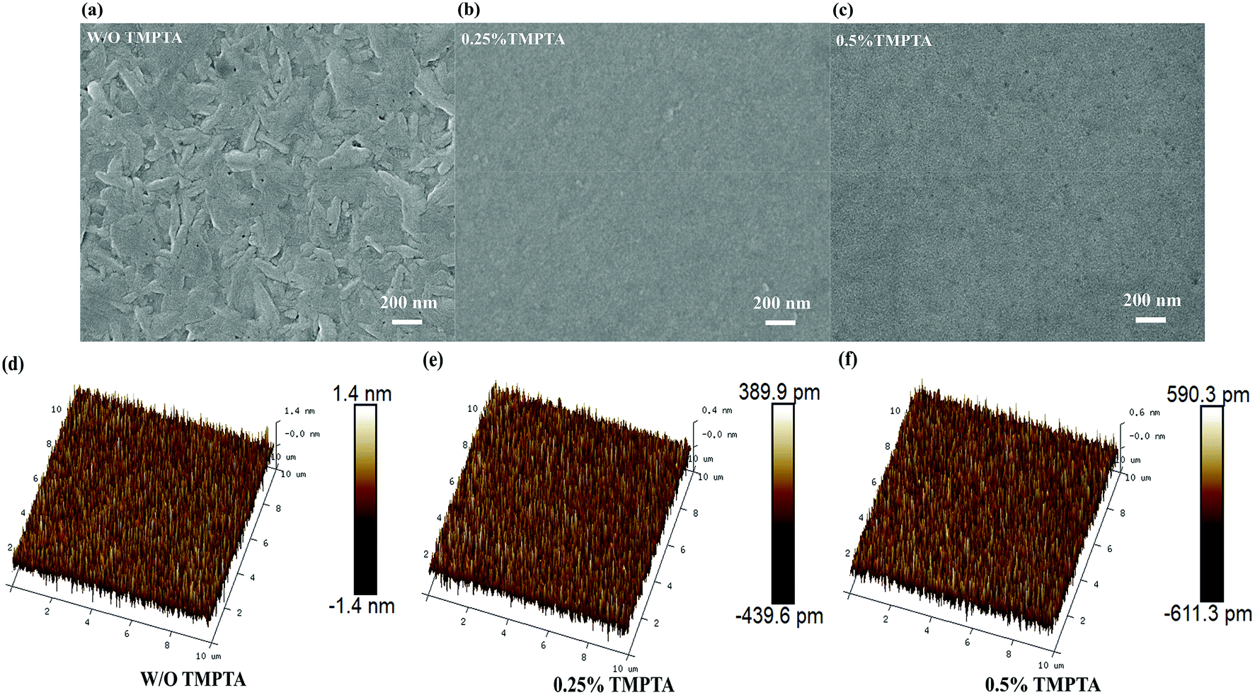 | ||
| Fig. 3 (a–c) Top-view SEM images and (d–f) 3D topographical AFM images of the quasi-2D perovskite films without or with TMPTA modification. | ||
X-ray diffraction (XRD) patterns were further characterized to learn the crystallinity of the quasi-2D perovskite films in Fig. 4a. In the standard perovskite film without TMPTA modification, both diffraction peaks from small n and large n phases (similar to 3D perovskite) can be observed. The diffraction peaks of CsPbBr3 and FAPbBr3 can be seen at 2θ of 22.3° and 33.6°,30–32 respectively, the full widths at half maximum (FWHM) of the peaks are 0.351° and 0.592°, respectively. After adding TMPTA, the positions of the diffraction peaks have not changed. The FWHMs of CsPbBr3 and FAPbBr3 increase correspondingly, which are 0.351° and 0.682°, respectively. These indicate that TMPTA does not change the lattice structure of the inner CsFAPbBr3 layers, while it makes the grain size smaller. With TMPTA modification (0.25% condition), the diffraction peak from n = 2 near 12.2° is suppressed. Meanwhile, the diffraction peak from TMPTA at 33.1° is also observed, revealing the existence of TMPTA in the modified perovskite film. These indicate that the modification of TMPTA in the crystallization process may modify the film quality and change the phase impurity of the perovskite film. To verify this, the absorption spectra of the quasi-2D perovskite film are shown in Fig. 4b. It can be seen that the quasi-2D perovskite film without TMPTA modification suffers obvious phase impurity, i.e., the absorption from n = 2, 3, 4 at short wavelengths and large n phases at the absorption edge can be observed. Compared to TMPTA modification, the absorption from small and large n phases are minimized and the absorption edge is blue shifted. This reveals that the phase impurity is reduced by TMPTA modification.
 | ||
| Fig. 4 (a) XRD patterns, (b) absorption spectra, (c) PL spectra and (d) normalized PL spectra of the quasi-2D perovskite films modified without and with 0.25% TMPTA. Inset of (c) is the photograph of the quasi-2D perovskite films excited by an ultraviolet lamp with a wavelength of 365 nm. | ||
The reduced phase impurity benefits from increasing the perovskite film's radiative efficiency, which can be further proved by photoluminescence (PL) measurements. As shown in Fig. 4c and d, the PL intensity of the main emission peak is enhanced, and the emission intensity is enhanced as revealed by the photographs inset Fig. 4c under excitation of an ultraviolet lamp; meanwhile, the emission from n = 2 phase at 438 nm is suppressed. Moreover, the peak wavelength (λPL) of the main emission peak is blue shifted from 525 nm to 516 nm. This blue shift is by that of the EL emission peak and the absorption edge. Therefore, it can be concluded that TMPTA modification can inhibit the formation of unexpected n phases and increase PL efficiency.
Time-resolved PL (TRPL) decay profiles of the quasi-2D perovskite films are shown in Fig. 5a, which reveal the reduced nonradiative recombination in perovskite films by TMPTA modification. The average carrier lifetimes of the films without and with 0.25%, 0.5% TMPTP modification are 5.97 ns, 7.01 ns, 10.51 ns, respectively. The carrier lifetime is governed by both the radiative recombination and nonradiative recombination rates. Decreasing both of them can be responsible for increasing the resultant carrier lifetime. In the condition of TMPTA modification, the radiative rate can not be reduced, as TMPTA modification makes the grain size much smaller, which may lead to the enhanced confinement of carriers inside the grain and increase the radiative recombination rate. Hence, the increase of the carrier lifetime is induced by the decreased nonradiative recombination rate. The reduced nonradiative recombination rate increase the PL intensity and PL quantum yield (PLQY), especially in the condition of 0.25% TMPTA, as revealed by Fig. 4c and 5b. The decreased nonradiative recombination rate may correlate with two functions of TMPTA: (1) reducing phase impurity as revealed by the absorption and PL spectra shown in Fig. 4b–d, which minimizes the carrier recombination on less efficient large n phases; (2) defect passivation through ester functional groups, which can form bonds with charged defects and thus inhibit nonradiative recombination.
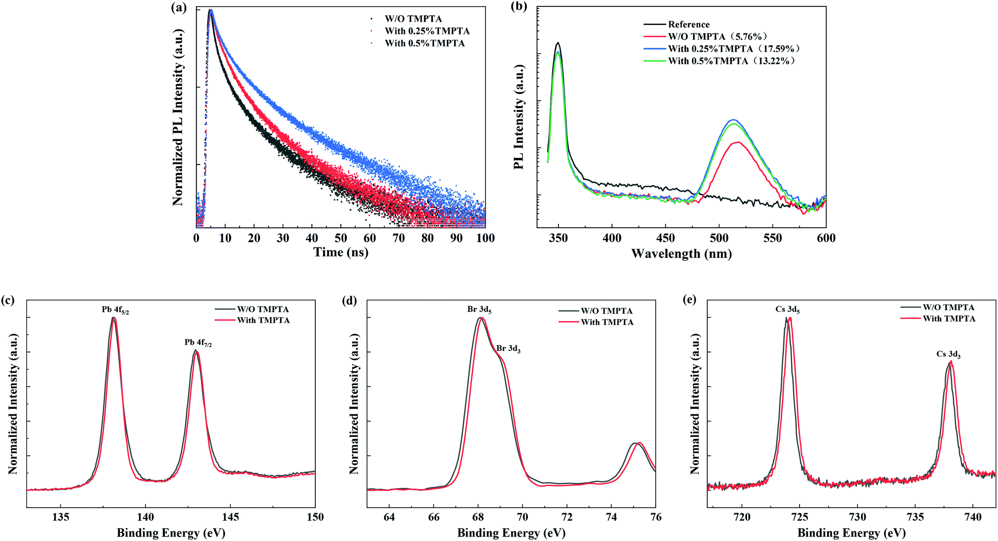 | ||
| Fig. 5 (a) Time-resolved PL (TRPL) decay profiles, (b) PL quantum yield, and (c–e) XPS spectra from Pb 4f, Br 3d, and Cs 3d orbitals of the quasi-2D perovskite films without and with TMPTA modification (0.25%). | ||
In order to verify the bonding between ester groups of TMPTA and the possible charged defects, we measured the Fourier transform infrared (FTIR) spectra from pure TMTPA, individual substances that existed in the perovskite precursor (including PbBr2, CsBr, FABr, PEABr), the perovskite precursor and their mixed solutions in DMSO solvent. As shown in Fig. S1,† by mixing TMPTA and individual substances that existed in the perovskite precursor, it is found that the absorption peak of the CO bond shows detectable shifts, indicating the coordination of CO with the ions in the perovskite precursor. Moreover, X-ray photoelectron spectra (XPS) also reveal the function of TMPTA on the perovskite film, as shown in Fig. 5c–e, which show the shifts in the binding energies of Pb 4f, Br 3d, and Cs 3d orbitals. In principle, the shifts of Pb 4f, Br 3d, and Cs 3d orbitals to their higher binding energies by TMPTA modification indicate the reduced electron density on these elements. Considering the interactions of CO functional group of TMPTA and these ions as revealed by FTIR, the shifts in binding energies induced by TMPTA are probably induced by much stronger interaction between these elements and the CO functional group of TMPTA. Here, a larger shift in the binding energy of Cs 3d orbitals probably indicate that TMPTA interacts more with Cs+ at the perovskite surface. Hence, it can be deduced that the introduction of TMPTA in the antisolvent can coordinate with the ions like Pb2+ in the perovskite precursor and passivates the charged defects in the perovskite film through its CO functional groups. The passivation effect by TMPTA contributes to the enhanced PL intensity and prolonged carrier lifetime.
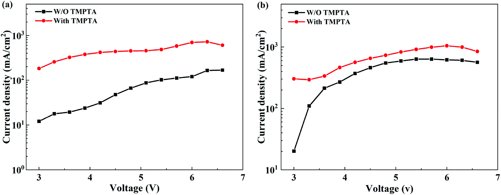
The improved film quality and the reduced phase impurity favor carrier transport in the perovskite EML, increasing current density at certain voltages. Hence, we use a single carrier device to verify the role of TMPTA in the carrier transport process. The structure of the electron-only device is ITO/ZnO/perovskite/TPBi (10 nm)/LiF (0.8 nm)/Al (100 nm), while that the hole-only device is ITO/m-PEDOT:PSS/perovskite/MoO3 (10 nm)/Al (100 nm). As shown in Fig. 6a and b, the electron current density is greatly improved with TMPTA modification, and the hole current density is also increased. These indicate that TMPTA modification can indeed improve carrier transport.
 | ||
| Fig. 6 Current density–voltage curves from (a) electron-only and (b) hole-only devices without or with TMPTA modification (0.25%). | ||
Electrochemical impedance spectra (EIS) were also measured to show the changes in the carrier dynamics by TMPTA modification. As shown in Fig. 7a, the recombination resistance (R-rec presented in the equivalent circuit) of the PeLED determined by the diameter of the semicircle in the EIS spectra is greatly decreased, benefiting from the reduced carrier recombination and the improved carrier transport in the perovskite EML. Furthermore, the EIS spectra from degraded PeLEDs were also measured. As shown in Fig. 7a, the recombination resistance increased after aging, leading to the degraded device performance. The increased recombination resistance can be induced by the increased defects inside the perovskite layer either through the increased point defects, the enhanced phase impurity and/or the morphology evolution of the film. To get further insights into these possible origins, we measured the PL spectra of the perovskite films from the fresh and the degraded devices. As shown in Fig. 7b, the main emission peaks of these devices show a negligible change in the peak wavelength and width. As the enhanced phase impurity typically induces emission at short wavelengths and the red shift in the main emission peak, the negligible change indicates that the phase impurity may not be enhanced during the degradation process, and it is not the main origin for the device degradation. The emission locates at the wavelengths shorter than 450 nm deriving from the intrinsic emission from TPBi, as it may not be washed away clearly. The morphology evolution of the perovskite films was characterized by AFM, as shown in Fig. 7c–f. The perovskite films generally show a minor change in the morphology without pinholes or other detectable changes arising. Hence, the degradation of the PeLEDs may mainly derive from the increased point defects in the perovskite layer. The point defects can be the result of slight material degradation, irreversible ion migration, etc. TMPTA can passivate the defects and confine the mobile ions by interacting with them, enhancing the device's stability.
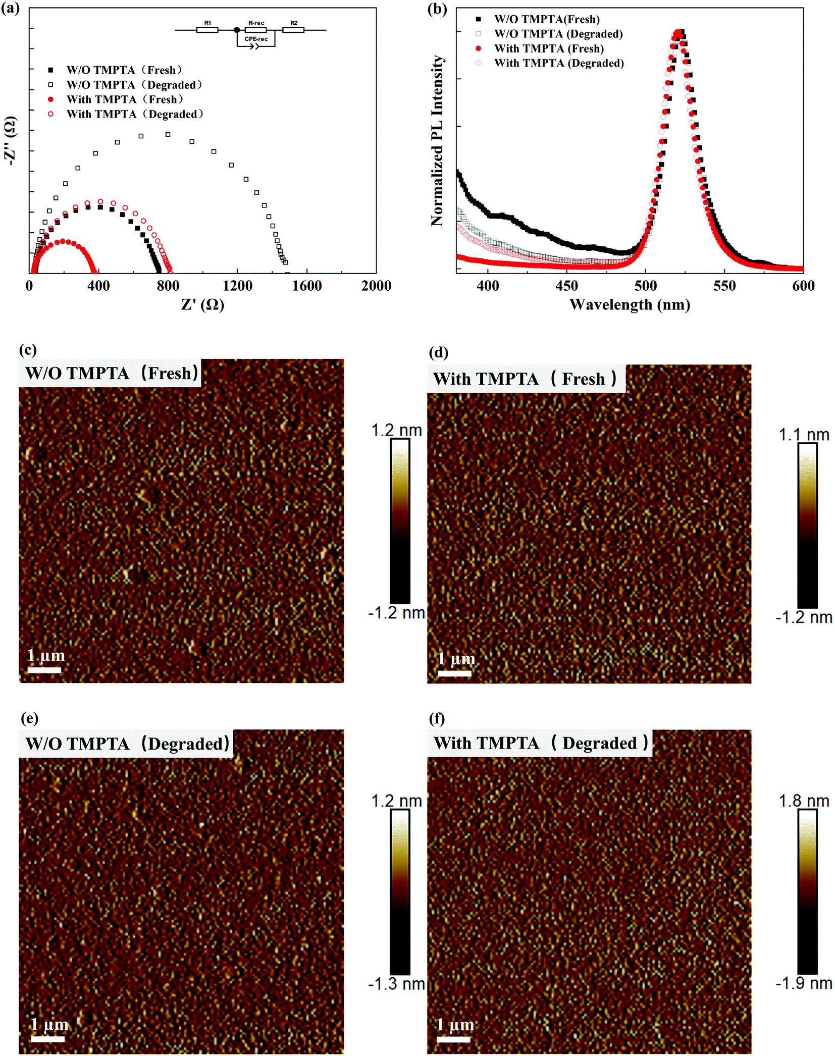 | ||
| Fig. 7 (a) EIS spectra of the PeLEDs without and with TMPTA modification before and after aging. (b) PL spectra and (c–f) AFM images of the perovskite films obtained from the fresh and degraded PeLEDs. The perovskite films were obtained by peeling off the metal cathode and washing away the organic electron transport materials. | ||
In addition, TMPTA modification is also proved to be efficient in other antisolvents like the typically used chlorobenzene (CB) antisolvent. The EL performance of the PeLEDs fabricated using CB as the antisolvent is shown in Fig. S2.† The device performance is also improved by TMPTA modification. The device efficiency is lower than that using EA solvent, which may be due to the intermiscibility between TMPTA and EA as they both have methyl groups. TMPTA can better passivate perovskite defects by penetrating the film with EA. Similar film quality improvements are observed by SEM images and XRD patterns shown in Fig. S3 and S4.† The films with TMPTA modification are also dense and uniform.
To verify the universality of TMPTA in different perovskite systems, TMPTA was added to the CsPbBr3 precursor solution to fabricate 3D inorganic perovskite EML. It is found that TMPTA can also improve the EL performance of the device, as shown in Fig. S5.† At the same time, the SEM images of the perovskite film shown in Fig. S6† reveal that TMPTA can also improve the quality of the perovskite film, making the grains more uniform. Therefore, TMPTA can be used as an effective material to improve the performance of PeLEDs.
4. Conclusion
In this work, when the volume ratio of the insulating organic small molecule TMPTA added to the antisolvent is 0.25%, the device obtains the best performance. The maximum luminance is 14790 cd m−2, the maximum current efficiency is 22.3 cd A−1, and the maximum EQE is 6.05%. By dissolving in the antisolvent, TMPTA improves the film quality and reduces the phase impurity of the quasi-2D perovskite layer, together with its defect passivation functional through the ester groups leading to increased device efficiency and stability. TMPTA is also effective in other perovskite films, proving its universality in modifying the perovskite layer. This work provides an efficient approach to improve the device performance of PeLEDs and highlights the importance of improving the phase impurity in quasi-2D perovskite films.
Conflicts of interest
There are no conflicts to declare.Acknowledgements
This work was supported by Beijing Natural Science Foundation No. 2192045, the National Natural Science Foundation of China under Grant No. 61775013, and 62075006, the Educational Research Project of Young and Middle-Aged Teachers in Fujian Province No. JAT190072, National Natural Science Foundation No. 52002070.Notes and references
- K. Y. Yang, F. S. Li, H. L. Hu, T. L. Guo and T. W. Kim, Nano Energy, 2019, 65, 104029 CrossRef CAS.
- J. E. Jeong, J. H. Park, C. H. Jang, M. H. Song and H. Y. Woo, Adv. Mater., 2020, 32, 2002176 CrossRef CAS PubMed.
- V. Adinolfi, W. Peng, G. Walters, O. M. Bakr and E. H. Sargent, Adv. Mater., 2018, 30, 1700764 CrossRef PubMed.
- V. D'Innocenzo, A. R. Srimath Kandada, M. De Bastiani, M. Gandini and A. Petrozza, J. Am. Chem. Soc., 2014, 136, 17730–17733 CrossRef PubMed.
- Z. Xiao, R. A. Kerner, L. Zhao, N. L. Tran, K. M. Lee, T.-W. Koh, G. D. Scholes and B. P. Rand, Nat. Photonics, 2017, 11, 108–115 CrossRef CAS.
- M. Yang, T. Zhang, P. Schulz, Z. Li, G. Li, D. H. Kim, N. Guo, J. J. Berry, K. Zhu and Y. Zhao, Nat. Commun., 2016, 7, 12305 CrossRef CAS PubMed.
- S. Yakunin, M. Sytnyk, D. Kriegner, S. Shrestha, M. Richter, G. J. Matt, H. Azimi, C. J. Brabec, J. Stangl, M. V. Kovalenko and W. Heiss, Nat. Photonics, 2015, 9, 444–449 CrossRef CAS PubMed.
- S. W. Eaton, M. Lai, N. A. Gibson, A. B. Wong, L. Dou, J. Ma, L. W. Wang, S. R. Leone and P. Yang, Proc. Natl. Acad. Sci. U. S. A., 2016, 113, 1993–1998 CrossRef CAS PubMed.
- K. Shibuya, M. Koshimizu, H. Murakami, Y. Muroya, Y. Katsumura and K. Asai, J. Appl. Phys., 2004, 43, L1333–L1336 CrossRef.
- S. Zhang, C. Yi, N. Wang, Y. Sun, W. Zou, Y. Wei, Y. Cao, Y. Miao, R. Li, Y. Yin, N. Zhao, J. Wang and W. Huang, Adv. Mater., 2017, 29, 1606600 CrossRef PubMed.
- B. Traore, L. Pedesseau, L. Assam, X. Che, J. C. Blancon, H. Tsai, W. Nie, C. C. Stoumpos, M. G. Kanatzidis, S. Tretiak, A. D. Mohite, J. Even, M. Kepenekian and C. Katan, ACS Nano, 2018, 12, 3321–3332 CrossRef CAS PubMed.
- B. Liu, X. Zou, D. Chen, T. Liu, Y. Zuo, J. Zheng, Z. Liu and B. Cheng, Tsinghua Sci. Technol., 2021, 26, 496–504 CAS.
- H. Yue, D. Song, S. Zhao, Z. Xu, B. Qiao, S. Wu and J. Meng, RSC Adv., 2019, 9, 8373–8378 RSC.
- Y. Huang, W. Luan, M. Liu and L. Turyanska, J. Mater. Chem. C, 2020, 8, 2381–2387 RSC.
- Q. Wang, J. Ren, X. F. Peng, X. X. Ji and X. H. Yang, ACS Appl. Mater. Interfaces, 2017, 9, 29901–29906 CrossRef CAS PubMed.
- M. Karlsson, Z. Yi, S. Reichert, X. Luo, W. Lin, Z. Zhang, C. Bao, R. Zhang, S. Bai, G. Zheng, P. Teng, L. Duan, Y. Lu, K. Zheng, T. Pullerits, C. Deibel, W. Xu, R. Friend and F. Gao, Nat. Commun., 2021, 12, 361 CrossRef CAS PubMed.
- X. Yang, X. Zhang, J. Deng, Z. Chu, Q. Jiang, J. Meng, P. Wang, L. Zhang, Z. Yin and J. You, Nat. Commun., 2018, 9, 570 CrossRef PubMed.
- H. Kim, K. A. Huynh, S. Y. Kim, Q. V. Le and H. W. Jang, Phys. Status Solidi RRL, 2019, 14, 1900435 CrossRef.
- P. Chen, Y. Meng, M. Ahmadi, Q. Peng, C. Gao, L. Xu, M. Shao, Z. Xiong and B. Hu, Nano Energy, 2018, 50, 615–622 CrossRef CAS.
- Q. Xu, R. Wang, Y.-L. Jia, X.-L. He, Y.-H. Deng, F.-X. Yu, Y. Zhang, X.-J. Ma, P. Chen, Y. Zhang, Z.-H. Xiong and C.-H. Gao, Org. Electron., 2021, 98, 10629 CrossRef.
- A. Z. Chen and J. J. Choi, J. Vac. Sci. Technol., 2020, 38, 010801 CrossRef CAS.
- D. Zhang, Y. Fu, C. Liu, C. Zhao, X. Gao, J. Zhang, W. Guo, J. Liu, C. Qin and L. Wang, Adv. Funct. Mater., 2021, 31, 2103890 CrossRef CAS.
- G. Wu, X. Li, J. Zhou, J. Zhang, X. Zhang, X. Leng, P. Wang, M. Chen, D. Zhang, K. Zhao, S. F. Liu, H. Zhou and Y. Zhang, Adv. Mater., 2019, 31, 1903889 CrossRef CAS PubMed.
- J. Hu, I. W. H. Oswald, S. J. Stuard, M. M. Nahid, N. Zhou, O. F. Williams, Z. Guo, L. Yan, H. Hu, Z. Chen, X. Xiao, Y. Lin, Z. Yang, J. Huang, A. M. Moran, H. Ade, J. R. Neilson and W. You, Nat. Commun., 2019, 10, 1276 CrossRef PubMed.
- P. Mao, J. Zhuang, Y. Wei, N. Chen, Y. Luan and J. Wang, Sol. RRL, 2019, 3, 1800357 CrossRef.
- Y. Hu, L. M. Spies, D. Alonso-Álvarez, P. Mocherla, H. Jones, J. Hanisch, T. Bein, P. R. F. Barnes and P. Docampo, J. Mater. Chem. A, 2018, 6, 22215–22225 RSC.
- Trimethylolpropane trimethacrylate, https://pubchem.ncbi.nlm.nih.gov/compound/18689#section=Chemical-and-Physical-Properties, accessed 17 October 2021.
- A. Liang, K. Wang, Y. Gao, B. P. Finkenauer, C. Zhu, L. Jin, L. Huang and L. Dou, Angew. Chem., Int. Ed., 2021, 60, 8337–8343 CrossRef CAS PubMed.
- X. Peng, X. Yang, D. Liu, T. Zhang, Y. Yang, C. Qin, F. Wang, L. Chen and S. Li, ACS Energy Lett., 2021, 6, 4187–4194 CrossRef CAS.
- D. Han, M. Imran, M. Zhang, S. Chang, X. G. Wu, X. Zhang, J. Tang, M. Wang, S. Ali, X. Li, G. Yu, J. Han, L. Wang, B. Zou and H. Zhong, ACS Nano, 2018, 12, 8808–8816 CrossRef CAS PubMed.
- H. Alehdaghi, A. Kanwat, M. Zirak, E. Moyen, W.-C. Choi and J. Jang, Org. Electron., 2020, 79, 105626 CrossRef CAS.
- J. Wang, C. Song, Z. He, C. Mai, G. Xie, L. Mu, Y. Cun, J. Li, J. Wang, J. Peng and Y. Cao, Adv. Mater., 2018, 30, 1804137 CrossRef PubMed.
Footnote |
| † Electronic supplementary information (ESI) available. See DOI: 10.1039/d1ra09040b |
| This journal is © The Royal Society of Chemistry 2022 |