
 Open Access Article
 This Open Access Article is licensed under a Creative Commons Attribution-Non Commercial 3.0 Unported Licence
Improved microstructure and significantly enhanced dielectric properties of Al3+/Cr3+/Ta5+ triple-doped TiO2 ceramics by Re-balancing charge compensation
Porntip Siriyaa,
Atip Pengpada,
Pornjuk Srepusharawoot a,
Narong Chanlekb and
Prasit Thongbai*a
a,
Narong Chanlekb and
Prasit Thongbai*a
aGiant Dielectric and Computational Design Research Group (GD-CDR), Department of Physics, Faculty of Science, Khon Kaen University, Khon Kaen 40002, Thailand. E-mail: pthongbai@kku.ac.th
bSynchrotron Light Research Institute (Public Organization), 111 University Avenue, Muang District, Nakhon Ratchasima 30000, Thailand
First published on 9th February 2022
Abstract
The charge compensation mechanism and dielectric properties of the (AlxCr0.05−x)Ta0.05Ti0.9O2 ceramics were studied. The mean grain size slightly changed with the increase in the Al3+/Cr3+ ratio, while the porosity was significantly reduced. The dielectric permittivity of the co-doped Cr0.05Ta0.05Ti0.9O2 ceramic was as low as ε′∼ 103, which was described by self-charge compensation between Cr3+–Ta5+, suppressing the formation of Ti3+. Interestingly, ε′ can be significantly increased (6.68 × 10⁴) by re-balancing the charge compensation via triple doping with Al3+ in the Al3+/Cr3+ ratio of 1.0, while a low loss tangent (∼0.07) was obtained. The insulating grains of [Cr0.053+Ta0.055+]Ti0.94+O12 has become the semiconducting grains for the triple-doped Alx3+[Cr0.05−x3+Ta0.05−x5+][Tax5+Tix3+Ti0.9+x4+]O12+3x/2. Considering an insulating grain with low ε′ of the Cr0.05Ta0.05Ti0.9O2 ceramic, the electron-pinned defect-dipoles and interfacial polarization were unlikely to exist supported by the first principles calculations. The significantly enhanced ε′ value of the triple-doped ceramic was primarily contributed by the interfacial polarization at the interface between the semiconducting and insulating parts, which was supported by impedance spectroscopy. This research gives an underlying mechanism on the charge compensation in the Al3+/Cr3+/Ta5+-doped TiO2 system for further designing the dielectric and electrical properties of TiO2-based ceramics for capacitor applications.
1. Introduction
Recently, a large number of accepter/donor co-doped TiO2 ceramics have been widely investigated due to a potential application in ceramic capacitors such as In3+/Nb5+,1–4 Al3+/Nb5+,5–7 Ga3+/Nb5+,8,9 Sc3+/Nb5+,10 Fe3+/Nb5+,11,12 Er3+/Nb5+,13,14 Zn2+/Nb5+,15,16 Dy3+/Nb5+,17 Gd3+/Nb5+,18 Mg2+/Nb5+,19,20 Ag+/Nb5+,21,22 Li+/Nb5+,23 Pr3+/Nb5+,24 Ga3+/Ta5+,25 Al3+/Ta5+,26 Mg2+/Ta5+,27,28 Co2+/Nb5+,29 and Bi3+/Sb5+ (ref. 30) co-doped TiO2 ceramics. All these ceramic systems exhibited a high dielectric constant (ε′ > 104), low loss tangent (tan![[thin space (1/6-em)]](https://www.rsc.org/images/entities/char_2009.gif) δ < 0.1), and good temperature stability of ε′. The giant dielectric (GD) behavior of these co-doped TiO2 systems have been explained using several models such as electron-pinned defect-dipoles (EPDDs),1,16,28 surface barrier layer capacitors (SBLCs),31,32 internal barrier layer capacitors (IBLCs),33–36 and small polaron hopping models.8
δ < 0.1), and good temperature stability of ε′. The giant dielectric (GD) behavior of these co-doped TiO2 systems have been explained using several models such as electron-pinned defect-dipoles (EPDDs),1,16,28 surface barrier layer capacitors (SBLCs),31,32 internal barrier layer capacitors (IBLCs),33–36 and small polaron hopping models.8
According to the previous studies, the Al3+/Nb5+ (ANTO) and Al3+/Ta5+ co-doped TiO2 (ATTO) ceramics with different co-doping concentrations can exhibit a high ε′ (>104) and low tanδ (<0.05).5–7,26 Using impedance spectroscopy, the semicircular arc of the grain (Rg) and grain boundary (Rgb) were found, which Rg ≪ Rgb.5,7,26 This means that the GD response of the ATTO ceramics is caused by the interfacial polarization between the semiconducting and insulating parts. On the other hand, the observed GD response with low tanδ in the Al3+/Nb5+ co-doped TiO2 (ANTO) with various co-doping concentrations.6 It was clearly demonstrated that the surface layer on the ANTO has a remarkable impact on the tanδ value, which would be increased after removing the surface layer. Accordingly, the important role of Al3+ is to form the insulative surface layer without the formation of oxygen vacancies.6 The GD response in the ANTO was further shown to be caused by the insulating grain boundaries (GBs),5,7 whereas the low tanδ was due to the synergistic effect of insulating GBs (IBLC) and insulative surface layer (SBLC).5–7,26
Most recently, the high ε′ (>104), low tanδ (∼0.06) as well as the ε′ value can be stable in the temperature range from −60 to 150 °C were achieved in the 1.0%Cr3+/Ta5+ co-doped TiO2 ceramics (1% CTTO).37 According to the first principles calculation and impedance spectroscopy, the GD properties of 1% CTTO were not attributed to the EPDD effect but can be described by internal polarization at the internal interfaces following the IBLC and SBLC effects. It was also found that the GD response in the CTTO decreased with the increase in the co-doping concentration, which might be due to the self-change compensation between the Cr3+ and Ta5+ doping ions as the co-doping concentration increased.37 Unfortunately, this issue has never been discussed in detail. On the other hand, the GD responses of the ATTO and ANTO tended to increase with the increase in the co-doping concentration,5,26 which might be due to the interstitial Al3+ ions. The formation of defects and charge compensation in rutile-TiO2 ceramics has great effects on their dielectric and electrical properties. Thus, it is important to study the possible mechanisms of the charge compensations in different co-doped TiO2 systems, which have different defect formations, to better understand the defect formation in co-doped rutile-TiO2 ceramics.
In the present study, the dielectric and electrical properties of Al3+/Cr3+/Ta5+ triple-doped TiO2 ceramics with various Al3+/Cr3+ doping ratios have been investigated. Their phase composition, microstructure, and chemical composition were systematically analyzed. Notably, a low ε′ value at 1 kHz of the Cr3+/Ta5+ co-doped TiO2 ceramic (∼1 × 10³) owing to the self-charge compensation between the dopants was greatly enhanced to 6.68 × 10⁴ by triple doping with Al3+, which was due to the re-balance of the charge compensation. Furthermore, the tanδ value at 1 kHz was decreased from 0.239 to 0.070.
2. Experimental details
Triple-doped AlxCr0.05−xTa0.05Ti0.9O2 ceramics with x = 0, 0.005, and 0.025, (abbreviated as the CTTO, ACTTO-1 and ACTTO-2, respectively) were prepared by a conventional solid–state reaction method. TiO2 (Sigma-Aldrich, >99.9% purity), Al2O3 (Sigma-Aldrich, 99.99% purity), Cr2O3 (Sigma-Aldrich, ≥98% purity), and Ta2O5 (Sigma-Aldrich, 99.99% purity) were used as the starting raw materials. A wet ball milling method was used to mix the starting oxides. First, the starting raw oxides (∼10 g) were mixed by the ball milling method in ethanol (50 mL) for 24 h using ZrO2 balls (2 mm in diameter) as a grinding media. Second, the ZrO2 balls were separated. Third, ethanol was evaporated in an oven at 90 °C for 24 h. Details of the preparation route were previously reported.26,37 Next, the mixture of dried powders was pressed into the pellets without calcination. Finally, all the pellet samples were sintered at 1450 °C for 5 h at a heating rate of 3 °C min−1 to form the ceramic samples.The phase composition and crystal structures of the sintered samples were analyzed by X-ray diffraction (XRD, PANalytical, EMPYREAN). Field emission scanning electron microscopy (FESEM, Helios nanoLab, G3 CX) and energy-dispersive X-ray analysis (EDS-Mapping) were used to characterize the surface morphologies and dopant distribution of the ceramic samples, respectively. The oxidation state was investigated by X-ray photoelectron spectroscopy (XPS, AXIS Ultra DLD, UK) at Synchrotron Light Research Institute (SLRI), Thailand.
The parallel plate electrodes on the as-sintered samples were coated with Ag paint by heating at 600 °C for 30 min. The dielectric properties of all the samples were quantified using an impedance analyzer (KEYSIGHT, E4990A) over the frequency and temperature ranges of 102–106 Hz and −60 to 210 °C, respectively. The impedance calculation of all the ceramic samples was as follows:
 | (1) |
3. Results and discussion
Fig. 1(a) shows the XRD patterns of all sintered ceramics. A rutile-TiO2 (JCPDS 21-1276)1,2,16 with no impurity phase was observed in all samples. Fig. 1(b) and (c) display the Rietveld profile fitting for the CTTO, ACTTO-1, and ACTTO-2 ceramics, respectively. The results are well-fitted with the goodness of fit (GOF) of ∼1.483–2.127. The lattice parameters (a and c values) and the structural data, which were obtained from the Rietveld refinement, are summarized in Table 1. For the CTTO, the a and c values are larger than those of the undoped TiO2 ceramic and Cr0.005Ta0.005Ti0.99O2.37 This result is due to the relatively large ionic radii of the Cr3+ (r6 = 61.5 pm) and Ta5+ (r6 = 64.0 pm) dopants compared to that of the Ti4+ (r6 = 60.5 pm)39 host ion and a high co-doping concentration. After the replacement of Cr3+ with Al3+, the a and c values slightly decreased with the increase in the Al3+/Cr3+ ratio concentration because of the relatively low ionic radius of Al3+ (r6 = 53.5 pm).26,39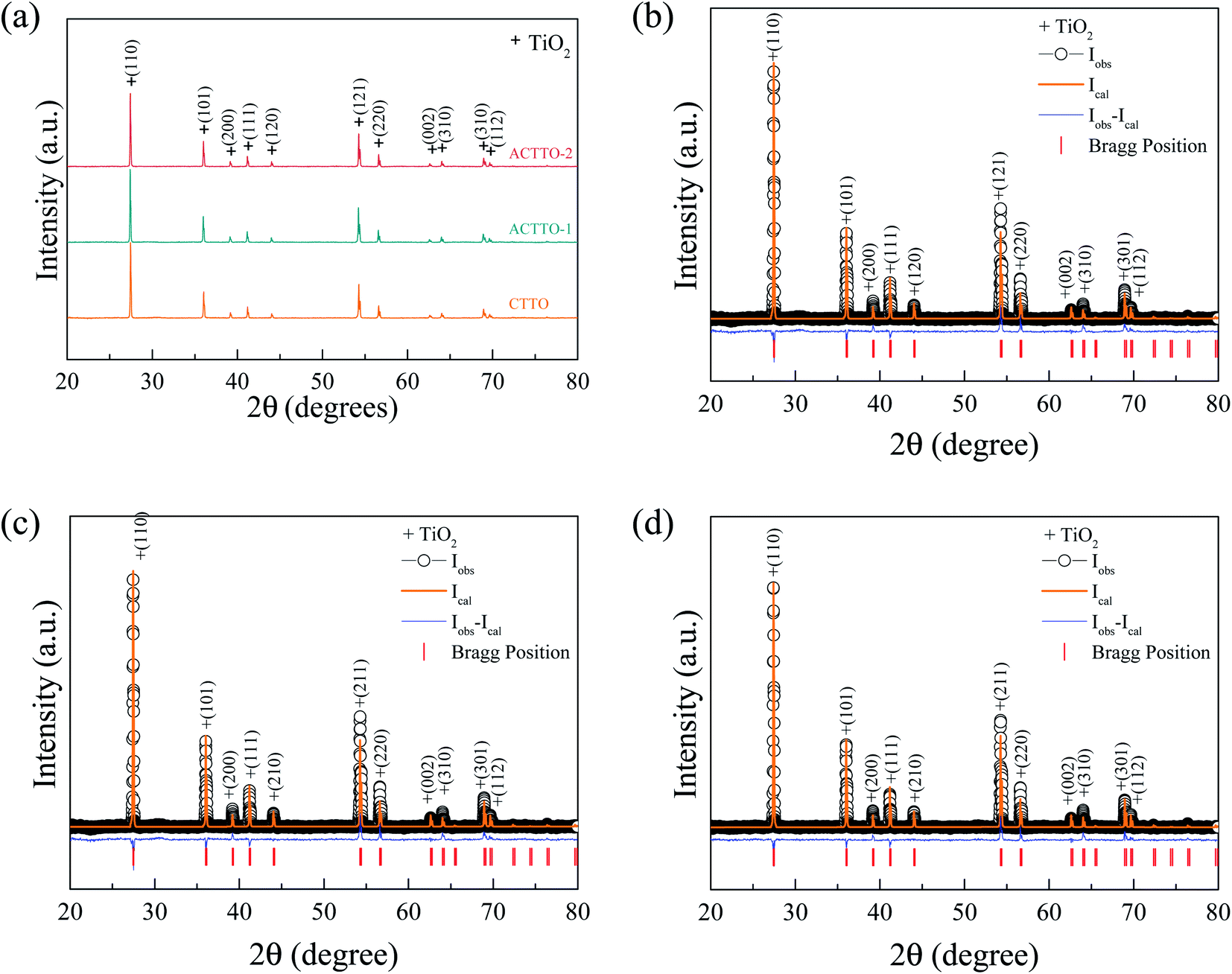 | ||
| Fig. 1 (a) XRD patterns of CTTO, ACTTO-1, and ACTTO-2 ceramics. (b–d) Rietveld profile fitting for CTTO, ACTTO-1, and ACTTO-2 ceramics, respectively. | ||
| Structural data/Ceramic samples | TiO2 | CTTO | ACTTO-1 | ACTTO-2 |
|---|---|---|---|---|
| a = b (Å) | 4.591(1) | 4.598(0) | 4.597(6) | 4.594(5) |
| c (Å) | 2.958(9) | 2.966(1) | 2.966(1) | 2.964(5) |
| GOF | 1.483 | 1.994 | 2.127 | 1.815 |
|
||||
| Bond length (Å), A = Ti, Al, Cr, Ta | ||||
| A(0,0,0)–O(0.19480,−0.19480,0.50000) | 1.946(0) | 1.950(0) | 1.950(0) | 1.949(0) |
| A(0,0,0)–O(0.30520,0.30520,0.00000) | 1.982(0) | 1.985(0) | 1.984(0) | 1.983(0) |
| A(0,0,0)–O(0.30520,−0.69480,0.00000) | 3.484(0) | 3.489(0) | 3.489(0) | 3.487(0) |
| A(0,0,0)–A(0,0,1) | 2.959(0) | 2.966(0) | 2.966(0) | 2.964(0) |
| Grain size (μm) | — | 5.8 ± 1.4 | 5.5 ± 1.5 | 7.0 ± 2.1 |
| Relative density (%) | — | 79.68 | 80.10 | 89.03 |
The most preferential rutile structure of the rutile-TiO2 structure doping with Al and Cr was studied via first principles calculations. As illustrated in Fig. 2, four different structures (S1–S4) of the Al- or Cr-doped TiO2 were designed by adding an oxygen vacancy (Vo). The total energies of different structures (S1–S4) were calculated by ΔE = E − E(S1), where E and E(S1) are total energies of various structures and structure,1 respectively. For the S1 structure, the triangular-shaped (2Al)VoTi or (2Cr)VoTi defect complex was set. This defect structure is the essential part of the EPDD structure,1 which will be formed only if (2Al)VoTi or (2Cr)VoTi was created and correlated to the diamond-shaped 2NbTi3+ATi (A = Ti4+/Ti3+/In3+) defect complex.40 In the S2–S4 structures, the different structures were designed without forming the triangular-shaped defect complex. According to the total energy calculations, the structures S2 and S3 of the Al- or Cr-doped TiO2 have the lowest total energy, respectively. For the S2 structure of the Al-doped TiO2, although two Al atoms prefer to occupy close together, they do not prefer to stay with Vo. Accordingly, this result indirectly indicated that the Al atom is an interstitial atom, which does not require Vo for charge compensation.6 Furthermore, the Cr atoms do not prefer to occupy close together. If Vo exists in the structure of the Cr-doped TiO2, the Cr atoms do not prefer to stay close to Vo. According to the fundamental concept, EPDDs cannot be formed in the AlxCr0.05−xTa0.05Ti0.9O2 structure. Thus, the dielectric properties of AlxCr0.05−xTa0.05Ti0.9O2 should be associated with the extrinsic effect of their ceramic microstructure.
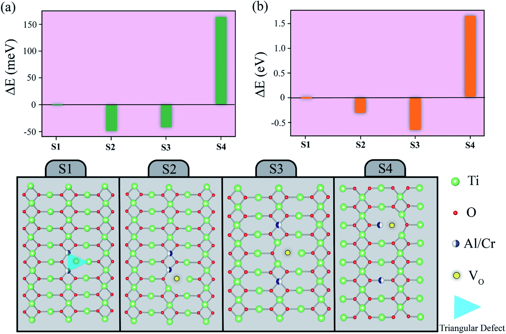 | ||
| Fig. 2 Total energies of different structures (S1–S4) for TiO2 substituted with Al and Cr atoms. | ||
As illustrated in Fig. 3, the grain shape of all the ceramics exhibited a relatively similar shape. Numerous small-sized pores in the CTTO ceramic are observed even when the ceramic was sintered at a temperature as high as 1450 °C for 5 h. This observation is in contrast to those reported in other co-doped TiO2 systems,9,10,20,21,25,35 which for a highly dense microstructure is usually obtained when sintering at high temperatures >1400 °C. This result indicates that the Cr3+ and Ta5+ dopants inhibited the sintering (or densification) rate of the TiO2 ceramic. Usually, the sintering rate of polycrystalline ceramic oxides is dependent on the diffusion rate of ions.41 The concentration of oxygen vacancies that were produced by the Cr3+ doping ions may not be high enough, which might be due to the self-charge compensation between the Cr3+ and Ta5+ dopants. Then, the number of pores decreased with the increase in the Al3+/Cr3+ ratio. This result is due to the increase in oxygen vacancies, which will be confirmed by the XPS technique in the next part. As shown in the inset of Fig. 3(a)–(c), the grain size distributions of all the sintered ceramics are narrow. The mean grain sizes of all the sintered ceramics are summarized in Table 1. The mean grain sizes of the CTTO and ACTTO-1 samples are nearly the same, while the mean grain size of the ACTTO-2 sample increased slightly compared to the CTTO sample. This result revealed that the Al3+/Cr3+ ratio has a slight effect on the grain growth, but it has a strong effect on the densification process.41 We reported that the Ta5+ dopant has a remarkable effect on the reduction in the grain size of the TiO2 ceramics,25,26,37 while the mean grain size of the Al3+-doped TiO2 was significantly increased compared to that of TiO2.26 The slightly increased mean grain size of ACTTO-2 was likely caused by the replacement of Cr3+ with Al3+.
 | ||
| Fig. 3 SEM images of the surface morphologies of (a) CTTO, (b) ACTTO-1, and (c) ACTTO-2 ceramics; insets show their grain size distribution. | ||
As demonstrated in Fig. 4, all dopant elements in the microstructures of the CTTO, which consisted of Cr and Ta dispersed well in both the grain and grain boundary of the CTTO and ACTTO-2. After triple-doping with Al, no segregation of any element in the grains and GBs was observed.
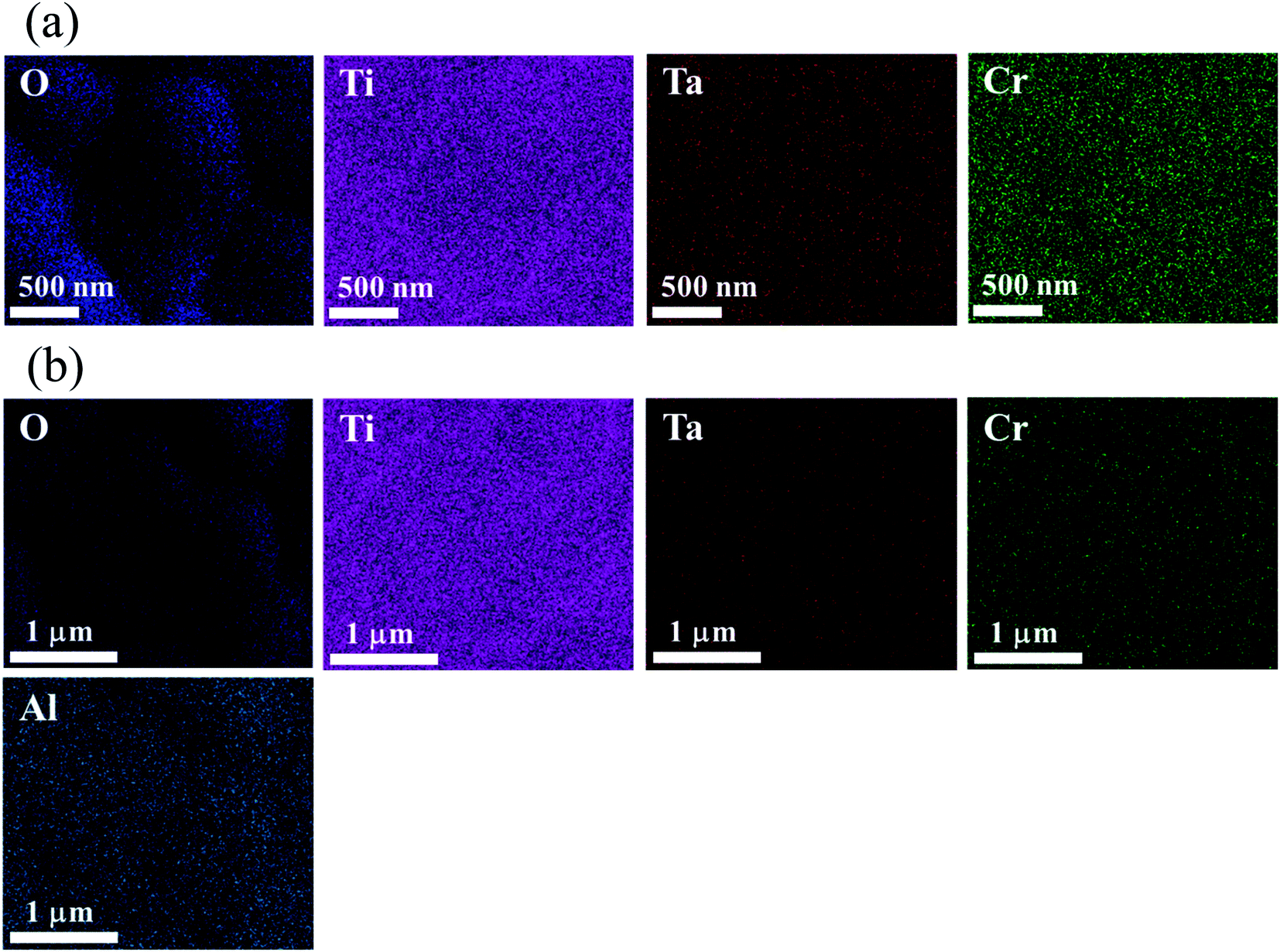 | ||
| Fig. 4 EDS-SEM mapping images of major and dopant element of (a) CTTO and (b) ACTTO-2 ceramics. | ||
Fig. 5 displays the frequency dependence of ε′ (at 25 °C). The dielectric parameters at 1 kHz of all the samples are summarized in Table 2. The ε′ values of the CTTO and ACTTO-1 (AlxCr0.05−xTa0.05Ti0.9O2 with x = 0.005, Al3+/Cr3+ ratio = 0.11) are nearly the same in value (∼103) over the measured frequency range. The ε′ value of the CTTO sintered at 1450 °C, co-doped with 10%(Cr + Ta), was much lower than that of the 1.0%(Cr + Ta) co-doped TiO2.37 As shown in the inset of Fig. 5, the tanδ values of the CTTO and ACTTO-1 are huge (>0.1), which is unsuitable for capacitor applications.2,42 This observation has never been explained in detail. Surprisingly, when increasing the Al3+/Cr3+ ratio to 1.0 (x = 0.025), the large ε′ of ∼6 × 10⁴ with a low tanδ of ∼0.07 was obtained. Such a large ε′ of ACTTO-2 can be comparable to those observed in several co-doped TiO2 ceramics.5,8,9,13,14,21,22,25,27–29,35,38 Furthermore, the rapid decrease in ε′ is observed at the frequency range of 104 Hz, indicating the additional polarization in the low-frequency range below 104 Hz. This result is caused by the replacement of a half Cr3+ with Al3+ ions. The significantly increased ε′ of ACTTO-2 may be correlated to a change in the charge compensation in the rutile-TiO2 structure, which were triple-doped with Al3+, Cr3+, and Ta5+.
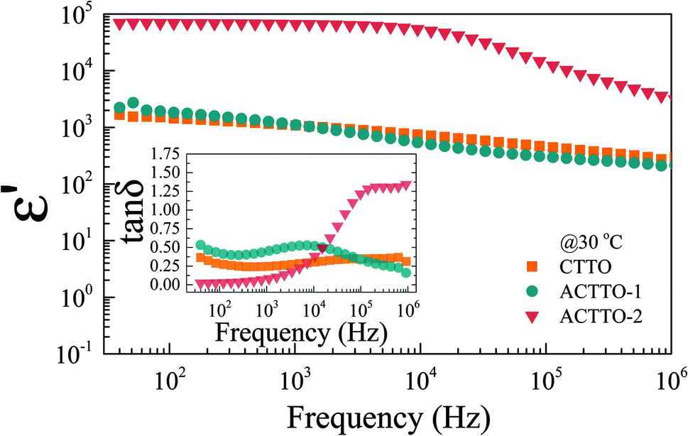 | ||
| Fig. 5 Frequency dependence of dielectric permittivity (ε′) at 30 °C of all ceramics; inset shows the frequency dependence of tanδ at 30 °C. | ||
δ) at 1 kHz, and activation energy of the insulating part (Ei) of all samples
| Sample | Dielectric Properties at 30 °C | Ei of the grain (eV) | |
|---|---|---|---|
| ε′ | tanδ |
||
| CTTO | 1080 | 0.239 | 0.705 |
| ACTTO-1 | 1107 | 0.442 | 0.686 |
| ACTTO-2 | 66811 |
0.070 | — |
Fig. 6 shows the temperature dependence of dielectric properties for all the samples. The ε′ values of CTTO and ACTTO-1 are strongly dependent on the temperature in the range from −60 to 210 °C. Notably, ACTTO-2 shows better temperature stability of ε′ than CTTO and ACTTO-1. As depicted in the inset of Fig. 6, two relaxation peaks of tanδ around 0 °C and 150 °C can be observed in the CTTO and ACTTO-1 samples, while only a low-temperature relaxation peak of the ACTTO-2 sample was observed. A low-temperature relaxation is likely associated with the dielectric response at the internal interfaces such as GBs and/or surface layer.2,27
 | ||
| Fig. 6 Temperature dependence of dielectric permittivity (ε′) at 103 Hz of all ceramics; inset shows the tanδ at 103 as a function of frequency. | ||
To clarify the origin of the abnormally enhanced GD properties of ACTTO-2 compared to that of CTTO and ACTTO-1, impedance spectroscopy was used to examine the electrical properties of the grains and GBs.5,7,32,35 As shown in Fig. 7(a) and (c), at −50 °C, a nonzero intercept on the Z′ axis in the complex impedance plane (Z*) of the CTTO and ACTTO plots disappeared. Only a part of a semicircular arc due to the grain response at high frequencies was found, indicating a large resistivity of the grains.43 When the measuring temperature was increased to 150 °C, the semicircular arc of the grain response can be observed in the Z* plots of CTTO and ACTTO-1. Furthermore, a tail of the relatively large semicircular arc of the GBs was observed.43 At 150 °C, the Rg values for CTTO and ACTTO-1 are about 3.5 × 10⁵ and 1.2 × 10⁵ Ω, respectively, indicating that the grains of these two samples are the insulators. This result indicates that there are no semiconducting grains in CTTO and ACTTO-1.1,43 For the In3+/Nb5+ co-doped TiO2,1 although the grains are insulators, the GD response was observed due to the creation of EPDDs. From the first principles calculation and impedance spectroscopy, the EPDDs and strong interfacial polarization cannot be pronounced in CTTO and ACTTO, giving rise to a low ε′ value. According to the previous study,37 we found that the semiconducting grains, which were confirmed by the observed nonzero intercept in Z* plots, can be created in the 1.0%(Cr + Ta) co-doped TiO2 sintered at 1400–1500 °C. This result means that there were no free charge carriers in the grains of CTTO and ACTTO-1. It is likely that with the increase in the co-doping concentration of Cr and Ta, self-charge compensation may occur, which can be expressed as follows:44
 | (2) |
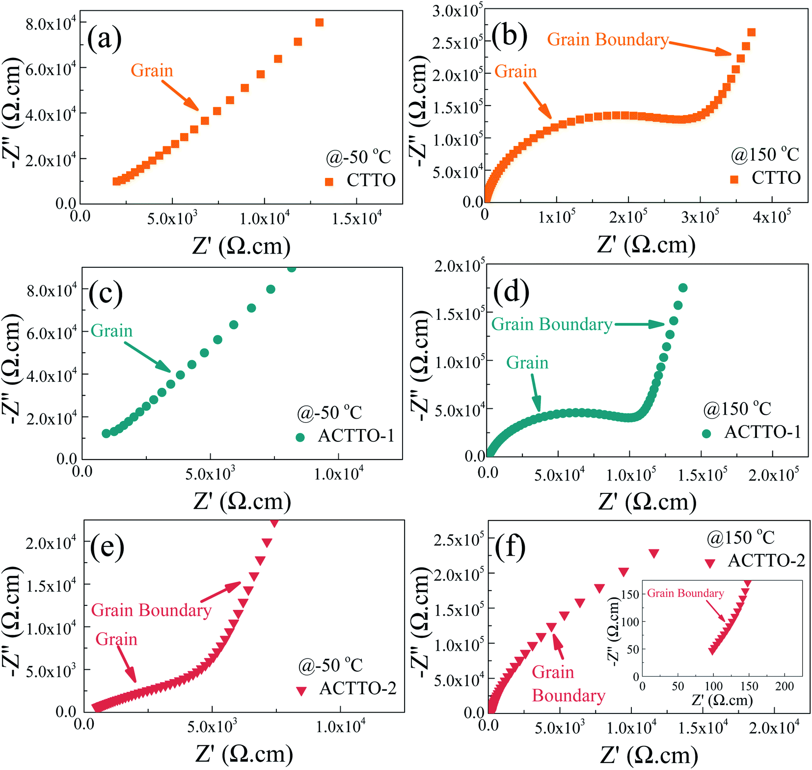 | ||
| Fig. 7 Impedance complex plane (Z*) plots at 50 °C and 150 °C of (a and b) CTTO, (c and d) ACTTO-1, and (e and f) ACTTO-2 ceramics; inset of (f) shows Z* plots at high frequencies. | ||
The charge balance equation of the 10%(Cr + Ta) co-doped TiO2 can be expressed as [Cr0.053+Ta0.055+]Ti0.94+O12. As summarized in Table 2, the Rg value of ACTTO-1 was reduced by a factor of ∼3 compared to that of CTTO. This result indicates that the replacement of Cr3+ with a small amount of Al3+ can cause an increase in the free charge carriers inside the grains. Furthermore, the conduction activation energies of the insulating grains (Ei) of CTTO and ACTTO-1 were calculated to be 0.705 and 0.686 eV, respectively. This decreased Ei is consistent with the observed decrease in Rg.
In contrast to those of CTTO and ACTTO-1, as shown in Fig. 7(e), a small arc can be observed in the Z* plot of the ACTTO-2 at −50 °C with Rg of ∼5 × 10³ Ω. At 150 °C, the large arc and nonzero intercept can be observed, as shown in Fig. 7(f) and its inset, respectively. The Rg value of ACTTO-2 was extremely reduced by three orders of magnitude compared to those of CTTO and ACTTO-1. The insulating grins of CTTO can be transformed to semiconducting grains by replacing a half of Cr3+ with Al3+.43 Therefore, the GD properties of ACTTO-2 are attributed to the interfacial polarization at internal interfaces such as insulating GBs and insulative outer surface layer.31,32,35 An applied electric field forces a large number of free charges in the semiconducting grains to move and accumulate at the insulating GB layers or surface layers, giving rise to the significantly increased ε′. According to the previous work6 and the first principles calculation in this study, the Al3+ doping ions did not prefer to occupy at the Ti4+ sites due to a relatively smaller ionic radius of Al3+. Instead, the Al3+ ions behave as interstitial ions. Thus, the charge compensation in the Al0.025Cr0.025Ta0.05Ti0.9O2 composition (ACTTO-2) has been re-balanced due to a relatively high concentration of the donor Ta5+ doping ions compared to that of the acceptor Cr3+ doping ions since Al3+ prefers to act as an interstitial ion rather than the doping ion. Accordingly, the self-charge compensation partially occurred, following the relationship Al0.0253+[Cr0.0253+Ta0.0255+][Ta0.0255+Ti0.0253+Ti0.9254+]O12.0375. Free electrons can be produced by the excessive Ta5+ doping ions (2.5%), following the equations:25,26
 | (3) |
| Ti4+ + e− → Ti3+ | (4) |
It is important to note that the critical role of the Al3+ doping ions is to produce the insulating layers on the outer surface6 and/or at the GBs.5,7 Song et al.7 have suggested that the Al3+ doping ions in AlxNb0.03Ti0.97−xO2 did not prefer to create a  structure. Hence, the role of Al3+ was not to form the EPDD in the rutile structure. They suggested that Al3+ acted as an acceptor dopant and captured the free electrons, which were produced by Nb5+. It is worth noting that the use of organic solvents such as ethanol in the milling process with precursors can generate surface defects.45
Furthermore, the substitution of TiO2 with Al3+ can produce the concentration gradient of Ti3+ from the outer surface to the inner core.6 No Ti3+ was detected on the outer surface, while more Ti3+ detected in the inner core. Fig. 8(a) and (b) show the XPS spectra of Ti 2p for the CTTO and ACTTO ceramics. As expected, Ti3+ cannot be fitted in the XPS spectra. For the CTTO ceramic, the disappearance on Ti3+ is due to the self-charge compensation between the Cr3+ and Ti5+ dopants, confirming the insulating grains in the Z* plot of the CTTO. On the other hand, for the ACTTO-2 ceramic, Al3+ doping into may cause the composition gradient of Ti3+ and Ti4+, just as reported in the Al3+/Nb5+ co-doped TiO2.6 The remarkably enhanced dielectric response in the triple-doped ceramic is therefore attributed to the re-balancing charge compensation. Fig. 8(c) and (d) illustrate the XPS spectra of O 1s of the CTTO and ACTTO-2 ceramics, respectively. For the CTTO and ACTTO-2 samples, the peak that referred to oxygen lattice (Ti–O) appeared at the binding energies of 529.94 and 530.15 eV, respectively.5,7,10,25 The oxygen vacancy  peak of the CTTO and ACTTO-2 samples was found at the binding energies of 531.68 and 531.89 eV,1,25 respectively. The percentage ratios of the
  and oxygen lattice for the CTTO and ACTTO-2 ceramics were about 8.90% and 13.03%, respectively. It is likely that the detected
  in the CTTO and ACTTO-2 ceramics may be caused by oxygen loss during the sintering at a high temperature.4,33 According to the impedance spectroscopy, the semiconducting grains of the CTTO ceramic was not formed due to the self-charge compensation between the dopants. Therefore, the disappearance of Ti3+ was likely caused by the charge compensation between Ti vacancy
  and
and  . According to the XPS results, the relative atomic percentage (%) ratio of Cr/Ta/Ti in the CTTO ceramic is 0.092/0.089/1.00, while that of the ACTTO-2 ceramic is 0.112/0.108/0.122/1.00. The Cr/Ti and Ta/Ti ratios of the CTTO ceramic are slightly higher than those of the theoretical ratio. It was found that the Al/Ti and Cr/Ti ratios of the ACTTO-2 ceramic are much higher than that of the theoretical ratio. Thus, this result may confirm the hypothesis that Al preferred to segregate near the surface on the ACTTO ceramics.
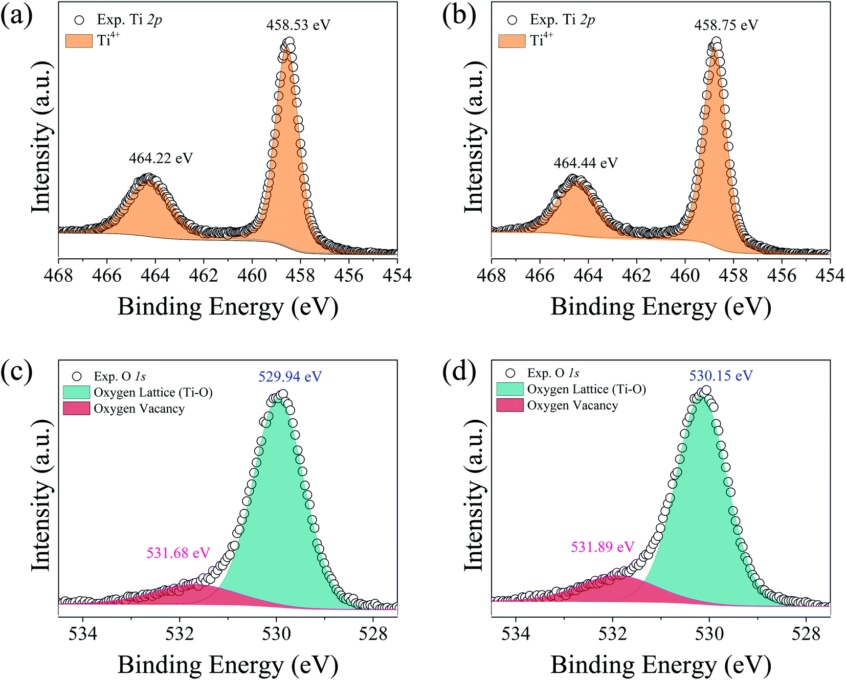 | ||
| Fig. 8 XPD spectra of Ti 2p for (a) CTTO and (b) ACTTO-2 ceramics and O 1s for (c) CTTO and (d) ACTTO-2 ceramics. | ||
4. Conclusions
The charge compensation of the (AlxCr0.05−x)Ta0.05Ti0.9O2 ceramics was re-balanced by increasing the Al3+/Cr3+ ratio to increase ε′. The increased Al3+/Cr3+ ratio caused a slight change in the mean grain size but had a pronounced effect on the densification process. The self-charge compensation between Cr3+–Ta5+ in (Cr0.05)Ta0.05Ti0.9O2 did not cause significant increase in the GD response due to the absence of Ti3+ (or very small amount) because it has a ε′ value of ∼103. The low ε′ value was due to a large Rg and very high conduction activation of the grains, which can create the interfacial polarization. Nevertheless, the ultra-high ε′ ∼ 6.68 × 10⁴ can be achieved by re-balancing the charge compensation via the partial replacement of Cr3+ with Al3+ with the Al3+/Cr3+ ratio of 1.0. The semiconducting grains can be produced due to the interstitial Al3+ ions. Hence, the self-charge compensation (Cr3+–Ta5+) has partially existed, and the Ta5+ left can produce the semiconducting grains. The GD properties were therefore attributed to the interfacial polarization at the interface between the semiconducting and insulating parts, as supported by impedance spectroscopy.Conflicts of interest
The authors declare no competing financial interests.Acknowledgements
This project is funded by the National Research Council of Thailand (NRCT): (N41A640084). This work has also received funding support from the Fundamental Fund of Khon Kaen University and the National Science, Research and Innovation Fund (NSRF). P. Siriya expresses her gratitude to the Science Achievement Scholarship of Thailand (SAST) for a PhD scholarship in Physics.References
- W. Hu, Y. Liu, R. L. Withers, T. J. Frankcombe, L. Norén, A. Snashall, M. Kitchin, P. Smith, B. Gong, H. Chen, J. Schiemer, F. Brink and J. Wong-Leung, Nat. Mater., 2013, 12, 821–826 CrossRef CAS PubMed.
- W. Tuichai, S. Danwittayakul, N. Chanlek, P. Srepusharawoot, P. Thongbai and S. Maensiri, RSC Adv., 2017, 7, 95–105 RSC.
- J. Li, Z. Xu, F. Li, X. Zhu and S. Zhang, RSC Adv., 2016, 6, 20074–20080 RSC.
- W. Tuichai, S. Danwittayakul, S. Maensiri and P. Thongbai, RSC Adv., 2016, 6, 5582–5589 RSC.
- G. Liu, H. Fan, J. Xu, Z. Liu and Y. Zhao, RSC Adv., 2016, 6, 48708–48714 RSC.
- W. Hu, K. Lau, Y. Liu, R. L. Withers, H. Chen, L. Fu, B. Gong and W. Hutchison, Chem. Mater., 2015, 27, 4934–4942 CrossRef CAS.
- Y. Song, X. Wang, X. Zhang, Y. Sui, Y. Zhang, Z. Liu, Z. Lv, Y. Wang, P. Xu and B. Song, J. Mater. Chem. C, 2016, 4, 6798–6805 RSC.
- W. Dong, W. Hu, A. Berlie, K. Lau, H. Chen, R. L. Withers and Y. Liu, ACS Appl. Mater. Interfaces, 2015, 7, 25321–25325 CrossRef CAS PubMed.
- W. Tuichai, S. Danwittayakul, J. Manyam, N. Chanlek, M. Takesada and P. Thongbai, Materialia, 2021, 18, 101175 CrossRef CAS.
- W. Tuichai, S. Danwittayakul, N. Chanlek, P. Thongbai and S. Maensiri, J. Alloys Compd., 2017, 703, 139–147 CrossRef CAS.
- T. Nachaithong, W. Tuichai, P. Moontragoon, N. Chanlek and P. Thongbai, Ceram. Int., 2018, 44, S186–S188 CrossRef CAS.
- T. Nachaithong, P. Moontragoon, N. Chanlek and P. Thongbai, RSC Adv., 2020, 10, 24784–24794 RSC.
- M.-Y. Tse, X. Wei and J. Hao, Phys. Chem. Chem. Phys., 2016, 18, 24270–24277 RSC.
- M.-Y. Tse, M.-K. Tsang, Y.-T. Wong, Y.-L. Chan and J. Hao, Appl. Phys. Lett., 2016, 109, 042903 CrossRef.
- N. Thongyong, W. Tuichai, N. Chanlek and P. Thongbai, Ceram. Int., 2017, 43, 15466–15471 CrossRef CAS.
- X. Wei, W. Jie, Z. Yang, F. Zheng, H. Zeng, Y. Liu and J. Hao, J. Mater. Chem. C, 2015, 3, 11005–11010 RSC.
- C. Zhao and J. Wu, ACS Appl. Mater. Interfaces, 2018, 10, 3680–3688 CrossRef CAS PubMed.
- Z. Cao, J. Zhao, J. Fan, G. Li and H. Zhang, Ceram. Int., 2021, 47, 6711–6719 CrossRef CAS.
- C. Yang, M.-Y. Tse, X. Wei and J. Hao, J. Mater. Chem. C, 2017, 5, 5170–5175 RSC.
- N. Thongyong, P. Srepusharawoot, W. Tuichai, N. Chanlek, V. Amornkitbamrung and P. Thongbai, Ceram. Int., 2018, 44, S145–S147 CrossRef CAS.
- P. Liang, J. Zhu, D. Wu, H. Peng, X. Chao and Z. Yang, J. Am. Ceram. Soc., 2021, 104, 2702–2710 CrossRef CAS.
- X. Zhou, P. Liang, J. Zhu, Z. Peng, X. Chao and Z. Yang, Ceram. Int., 2020, 46, 11921–11925 CrossRef CAS.
- W. Li, Z. Liu, F. Zhang, Q. Sun, Y. Liu and Y. Li, Ceram. Int., 2019, 45, 11920–11926 CrossRef CAS.
- Z. Liu, C. Zhao, B. Wu and J. Wu, Phys. Chem. Chem. Phys., 2018, 20, 21814–21821 RSC.
- W. Tuichai, N. Thongyong, S. Danwittayakul, N. Chanlek, P. Srepusharawoot, P. Thongbai and S. Maensiri, Mater. Des., 2017, 123, 15–23 CrossRef CAS.
- W. Tuichai, S. Danwittayakul, N. Chanlek and P. Thongbai, Mater. Res. Bull., 2019, 116, 137–142 CrossRef CAS.
- N. Thongyong, N. Chanlek, P. Srepusharawoot and P. Thongbai, Molecules, 2021, 26, 6952 CrossRef CAS.
- W. Dong, D. Chen, W. Hu, T. J. Frankcombe, H. Chen, C. Zhou, Z. Fu, X. Wei, Z. Xu, Z. Liu, Y. Li and Y. Liu, Sci. Rep., 2017, 7, 9950 CrossRef PubMed.
- T. Nachaithong, N. Chanlek, P. Moontragoon and P. Thongbai, Molecules, 2021, 26, 3230 CrossRef CAS PubMed.
- Z. Li and J. Wu, J. Materiomics, 2017, 3, 112–120 CrossRef.
- T. Nachaithong, P. Kidkhunthod, P. Thongbai and S. Maensiri, J. Am. Ceram. Soc., 2017, 100, 1452–1459 CrossRef CAS.
- T. Nachaithong, P. Thongbai and S. Maensiri, J. Eur. Ceram. Soc., 2017, 37, 655–660 CrossRef CAS.
- Y. Q. Wu, X. Zhao, J. L. Zhang, W. B. Su and J. Liu, Appl. Phys. Lett., 2015, 107, 242904 CrossRef.
- J. Li, F. Li, C. Li, G. Yang, Z. Xu and S. Zhang, Sci. Rep., 2015, 5, 8295 CrossRef CAS.
- W. Tuichai, S. Danwittayakul, N. Chanlek and P. Thongbai, J. Alloys Compd., 2017, 725, 310–317 CrossRef CAS.
- V. Bovtun, J. Petzelt, M. Kempa, D. Nuzhnyy, M. Savinov, S. Kamba, S. M. M. Yee and D. A. Crandles, Phys. Rev. Mater., 2018, 2, 075002 CrossRef CAS.
- W. Tuichai, S. Danwittayakul, N. Chanlek, M. Takesada, A. Pengpad, P. Srepusharawoot and P. Thongbai, ACS Omega, 2021, 6, 1901–1910 CrossRef CAS PubMed.
- W. Tuichai, S. Danwittayakul, P. Srepusharawoot, P. Thongbai and S. Maensiri, Ceram. Int., 2017, 43, S265–S269 CrossRef CAS.
- R. D. Shannon, Acta Crystallogr., Sect. A, 1976, 32, 751–767 CrossRef.
- C. C. Homes and T. Vogt, Nat. Mater., 2013, 12, 782–783 CrossRef CAS PubMed.
- M. N. Rahaman, Ceramic processing and sintering, M. Dekker, New York, 2nd edn, 2003 Search PubMed.
- Y. Wang, W. Jie, C. Yang, X. Wei and J. Hao, Adv. Funct. Mater., 2019, 29, 1808118 CrossRef.
- M. Li and D. C. Sinclair, J. Appl. Phys., 2013, 114, 034106 CrossRef.
- J. Boonlakhorn, N. Chanlek, J. Manyam, P. Srepusharawoot, S. Krongsuk and P. Thongbai, J. Adv. Ceram., 2021, 10, 1243–1255 CrossRef CAS.
- J. L. Clabel H, I. T. Awan, A. H. Pinto, I. C. Nogueira, V. D. N. Bezzon, E. R. Leite, D. T. Balogh, V. R. Mastelaro, S. O. Ferreira and E. Marega, Ceram. Int., 2020, 46, 2987–3001 CrossRef CAS.
| This journal is © The Royal Society of Chemistry 2022 |