 Open Access Article
High-performance ReS2 photodetectors enhanced by a ferroelectric field and strain field
Xiaochi Taiab,
Yan Chen *ac,
Shuaiqin Wua,
Hanxue Jiaoa,
Zhuangzhuang Cuia,
Dongyang Zhaoac,
Xinning Huanga,
Qianru Zhaoa,
Xudong Wanga,
Tie Lin*a,
Hong Shen
 *a,
Xiangjian Menga,
Jianlu Wanga and
Junhao Chuab
aState Key Laboratory of Infrared Physics, Shanghai Institute of Technical Physics, Chinese Academy of Sciences, 500 Yu Tian Road, Shanghai 200083, China. E-mail: lin_tie@mail.sitp.ac.cn; hongshen@mail.sitp.ac.cn
bSchool of Physical Science and Technology, ShanghaiTech University, Shanghai 201210, China
cDepartment of Materials, School of Physics and Electronic Science, East China Normal University, Shanghai 200241, China. E-mail: yanchen@ee.ecnu.edu.cn
First published on 9th February 2022
Abstract
Flexible optoelectronic devices have numerous applications in personal wearable devices, bionic detectors, and other systems. There is an urgent need for functional materials with appealing electrical and optoelectronic properties, stretchable electrodes with outstanding mechanical flexibility, and gate medium with flexibility and low power consumption. Two-dimensional transition metal dichalcogenides (TMDCs), a novel kind of widely studied optoelectrical material, have good flexibility for their ultrathin nature. P(VDF-TrFE) is a kind of organic material with good flexibility which has been proved to be a well-performing ferroelectric gate material for photodetectors. Herein, we directly fabricated a well-performing photodetector based on ReS2 and P(VDF-TrFE) on a flexible substrate. The device achieved a high responsivity of 11.3 A W−1 and a high detectivity of 1.7 × 10¹⁰ Jones from visible to near-infrared. Moreover, with strain modulation, the device's responsivity improved 2.6 times, while the detectivity improved 1.8 times. This research provides a prospect of flexible photodetectors in the near-infrared wavelength.
Introduction
During the past decade, two-dimensional (2D) transition metal dichalcogenides (TMDCs) have been widely studied owing to their unique properties, such as sizable bandgap,1,2 optimal detection,3,4 and ideal flexibility.5–7 While most people focus on group-6 TMDCs (MoS2, WS2, MoTe2, etc.),8 a newly emerging group-7 TMDC material, ReS2, has attracted much attention due to its unique thickness-independent direct band-gap (Eg ≈ 1.4 eV).9,10 Due to its unique 1T distorted structure, the interlayer coupling energy of ReS2 is much weaker than other TMDCs.9 The weak inter-layer coupling results in a continuous direct bandgap from bulk to monolayer, and the PL peak moves slightly (between 1.5 and 1.6 eV) with the intensity reduced. These properties made ReS2 and its heterostructures11–13 exhibit high performance in photodetectors. In addition, ReS2 and its heterostructures exhibit polarization-dependent photoresponse.14–16 To date, ReS2-based field effect transistors have been reported to have a switching ratio as high as 107,17 good detection performance (the photoresponsivity can reach up to 106 A W−1),18 and high response time up to 20 μs.19 However, in those traditional photodetectors, a constant high gate voltage (Vg) and a large drain-source current (Id) are applied to achieve good performance, which means high power consumption. Besides, the above devices used rigid dielectrics like oxides (Al2O3, SiO2, etc.). As a result, the device structures and constructed materials heavily limit practical applications in flexible photoelectric devices, such as artificial electronic skin,20 wearable systems,5 bionic detectors,21 etc. New dielectrics materials and new device structures are needed for further investigation to realize high-performance flexible devices.Organic ferroelectric material P(VDF-TrFE) is a promising option for gate dielectrics. Ferroelectric materials, such as α-In2Se3,22 LiNbO3,23 HfO2 (ref. 24) etc., has been proved to have good performance in ferroelectric field effect transistors (FeFETs). As to photodetectors, the ferroelectric field could increase the mobility, photoresponsivity, detectivity, and photoresponse speed.25 Moreover, after polarization, the remanent polarization is strong enough to keep the device working for months, which means low power consumption.26–28 On the other hand, as a solution-made organic material, it has huge potential for large-area flexible electronics. Previous researchers have made many nonvolatile memory devices29,30 and capacitors31–33 on flexible substrates to study the ferroelectric properties under strain.34,35 However, the electrical and photoelectrical properties of 2D materials & P(VDF-TrFE) based FeFET under strain have not been studied. Thus, a study on high-performance flexible photodetectors enhanced by ferroelectric field and strain field is necessary.
In this work, we fabricated a flexible ReS2/P(VDF-TrFE) hybrid photodetector on a polyimide (PI) substrate and investigated its detection performance in tensile condition. The electric and optoelectronic properties are studied under ferroelectric field. When the incident wavelength is 830 nm, the device with ferroelectric top gate on PI substrate exhibits a responsivity of 11.3 A W−1, and a detectivity of 1.7 × 10¹⁰ Jones without constant gate voltage. The response time reaches 6.1 ms. Under strain modulation, 2.6 times the responsivity of that without bending is achieved. When the device is released, the performance comes back to the initial level.
Experimental
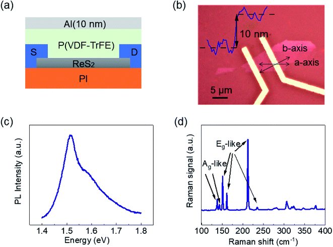
Fig. 1(a) and (b) is the structure schematic and the optical microscope photograph of the ReS2 photodetector, respectively. The few-layer ReS2 nanosheets were mechanically exfoliated from bulk ReS2 crystals (bought from Graphene) with an adhesive tape (Nitto tape) subsequently exfoliated with a polydimethylsiloxane (PDMS, Gelfilm from Gelpak) stamp. Several flakes with different thicknesses remain to adhere to the stamp and several flakes were transferred on the polyimide substrate. The regular-shaped flakes without wrinkles and cracks were chosen to form devices. This guaranteed strain applied evenly on devices. Next, the source (S) and drain (D) metal electrodes were fabricated using electron-beam lithography, thermal evaporation of Cr/Au films (15 nm/45 nm), and lift-off by acetone. The following step was coating the P(VDF-TrFE) (70![[thin space (1/6-em)]](https://www.rsc.org/images/entities/char_2009.gif) :
:![[thin space (1/6-em)]](https://www.rsc.org/images/entities/char_2009.gif) 30 in mol%) film as the top gate material. Finally, the ultrathin semitransparent aluminum (≈10 nm) electrodes were deposited. The thickness of ReS2 is further confirmed by atomic force microscopy (AFM). As shown in Fig. 1(b), the thickness of ReS2 is approximately 10 nm.
30 in mol%) film as the top gate material. Finally, the ultrathin semitransparent aluminum (≈10 nm) electrodes were deposited. The thickness of ReS2 is further confirmed by atomic force microscopy (AFM). As shown in Fig. 1(b), the thickness of ReS2 is approximately 10 nm.
Here we chose PI as the substrate for its heat stability ranging from −200 to 300 °C, poison-free, and insoluble in organic solvents. This means compatible with silicon processes and suitable for most situations. PI material and 2D materials have a good affinity, so that 2D materials are easy to adhere to the PI substrate. PI is suitable for bending for its elasticity modulus is up to 3–4 GPa. In addition, the 25 μm-thickness polyimide is suitable for control, because 2D materials on thick polyimide are hard to be bent and 2D materials on thin polyimide are easy to have wrinkles.
ReS2 flakes were analyzed via photoluminescence (PL) and Raman, which suggested the good quality of the multi-flakes as shown in Fig. 1(c) and (d). The PL peak obtained at ∼1.5 eV indicates the multi-layer nature of ReS2 showed in Fig. 1(c). In Fig. 1(d), we labeled two low frequencies Ag-like modes (located at 136.8 and 144.5 cm−1) corresponding to the out-of-plane vibrations of Re atoms and four Eg-like modes (located at 153.6, 163.4, 218.2, and 238.1 cm−1) corresponding to the in-plane vibrations of Re atoms. The rest 12 higher frequency Raman modes are vibrations mainly from lighter S atoms.36 This indicates that the ReS2 used in this study is a multi-layer sample.
Results and discussion
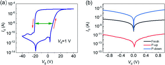
First, we studied how the remnant polarization enhances the device's electric properties. The thickness of the P(VDF-TrFE) layer is 300 nm (measured by Step Profiler). The transfer curves (Id–Vg) (drain-source current Id as a function of top gate voltage Vg) of the ReS2 transistor were tested at room temperature (shown in Fig. 2(a)). The large memory window (≈25 V) in transfer curves between the voltage rise and decrease is related to the ferroelectric polarization switching process. The mobility μ ≈ 115.3 cm2 V−1 s−1 was calculated bywhere L = 5.0 μm is the channel length, W = 2.0 μm is the channel width, εr = 10 is the dielectric constant of P(VDF-TrFE), d = 300 nm is the thickness of P(VDF-TrFE) films, and dId/dVg is extracted from the left side of the transfer curve in Fig. 2(a). The output characteristic curves Id–Vd of three different polarized states are showed in Fig. 2(b). The initial state of the P(VDF-TrFE) film is called fresh state. In this state, P(VDF-TrFE) film has not been polarized, and its dipoles are in disorder. No residual polarized electric field is generated, so it has little effect on the channel. A −40 V gate voltage applied made P(VDF-TrFE) film in polarization up state (P-up). The positive charges gather on the interface between P(VDF-TrFE) and ReS2. These positive charges would deplete the charges in channel. Then the carrier concentration is reduced and the dark current could be so low. Besides, the increase of the barrier also reduces the dark current. A 40 V gate voltage applied made P(VDF-TrFE) film in polarization down state (P-down). The negative charges gather on the interface and the channel was fully accumulated. Current in P-up state is five orders of magnitude smaller than current in P-down state. Operating the device in the P-up state brings the advantage of a reduced dark current.
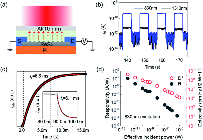
Next, the photoresponse of the ReS2 photodetector was measured at a ZERO gate voltage in the P-up state. As is shown in Fig. 3(a), the light at 830 nm is incident perpendicularly to the device surface, and the spot covers the entire channel uniformly. The ultrahigh local electrostatic field induced by the upward-polarized P(VDF-TrFE) makes the ReS2 channel fully depleted, which means the photodetector would have an ultra-low dark current. As a result, the ferroelectric field keeps the ReS2 photodetector at a sensitive state in a power efficient way. The photo switching properties (under Vd = 100 mV) at a wavelength of 830 nm and 1310 nm are shown in Fig. 3(b). The detector has good response for the wavelength of 830 nm light illumination and almost no response for 1310 nm. Fig. 3(c) shows the photocurrent exhibits rapid rise/fall and reaches a steady saturation. The rise (tr) and decay (tf) times of photocurrent are measured as 6.6 ms and 6.1 ms, respectively, and both the rise and decay curves (in black) are fitted well using a single exponential functions (in red) shown in Fig. 3(c). The responsivity R = Iph/Peff, where Iph is the photocurrent in a detector and Peff is the effective illumination power. It is worth mentioning that Peff is calculated by Peff = APπ−1r−2, where A is the area of the sample, P is the actual laser output and r is the radius of the laser spot size. In addition, the detectivity, assuming that noise from dark current is the major factor, is given by D* = RA1/2/(2eIdark)1/2, where R is the responsivity, A is the area of the detector, e is the unit charge, and Idark is the dark current (under 0.1 V bias here).24,37 The device exhibits a photoresponsivity (R) of 11.3 A W−1, and the detectivity (D*) is up to 1.7 × 10¹⁰ Jones approximately when the wavelength is 830 nm, a laser power of 1 pW, and Vd = 100 mV. The maximum detectivity of 1.7 × 10¹⁰ Jones has been achieved. As shown in Fig. 3(d), the high detectivity and responsivity decrease dramatically with the increasing signal power.
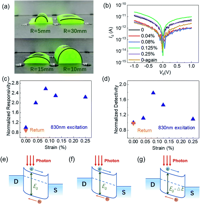
Based on the research of P(VDF-TrFE) based FeFET, the photoelectric properties under strain are studied. To apply strain on the devices, we made several half-cylinders printed by a 3D printer, then fixed the polyimide substrate on the curved surfaces (shown in Fig. 4(a)). The strains were quantified by the equation: ε = (t/r)/2,6 where t is the substrate thickness (25 μm for the PI substrates used here) and r is the bending radius of 30, 15, 10, 5 mm. Assuming that as-fabricated exfoliated devices before bending are virtually strain-free,38 we get five strains ε ≈ 0.00, 0.04, 0.08, 0.125, and 0.25%, respectively. The channel is along the b-axis (as shown in Fig. 1(b)), and so is the strain. This is the optimal option for strain modulation in this study. Fig. 4(b) shows the output characteristics of FeFET under different strains in dark state. The dark current went through a decrease under little strain and an increase when strain becomes larger. The ‘0’ state is the state before bending and after polarization. The ‘0-again’ state is the state return to ‘0’ state after bending. Fig. 4(c) shows the normalized photoresponsivity of the ReS2 phototransistor under strain. When a little strain is applied, the responsivity increases with the increase of strain. When the strain is 0.08%, the optical response reaches a maximum which is 2.6 times that strain is 0. The responsivity keeps a steady level when the strain is over 0.08%. Fig. 4(d) shows the normalized detectivity of the ReS2 phototransistor under strain. When the strain is 0.08%, the optical response reaches its maximum, which is 1.8 times that strain is 0. This means the device can achieve the best photoresponse with the 0.08% strain applied where the minimum dark current achieved. In addition, when the device was released, it was almost returned to its original state, and the process can be repeated.
Fig. 4(e)–(g) show the mechanism of strain modulation of the photodetector. The top electrode, P(VDF-TrFE) and ReS2 could be seen as a parallel plate capacitor. In a parallel plate capacitor, total quantity of electric charge (Q) is defined as Q = ε0εrSE, where ε0 is the permittivity of vacuum, εr is the relative permittivity, S is the area of plate and E is the electric field intensity. When a small strain applied, the electric field (E) provided by P(VDF-TrFE) is constant whereas the area (S) increases. This would lead to the increase of quantity of electric charge (Q). The increasing of Q at the interface between P(VDF-TrFE) and ReS2 would get more charges depleted. Thus, the carrier concentration reduces and the Fermi energy raises up. The dark current becomes lower then. With strain increase further, the dark current increases. The increase of dark current is mainly due to the narrowing of ReS2' bandgap. When the channel direction was made along the b-axis and the strain was applied along the channel direction, the decrease of the VBM is slower than that of the CBM, leading to the narrowing of the bandgap.36 As the carriers are fully depleted in P-up state, Ec − EF = Eg/2, where Ec is the conduction band edge, EF is the Fermi energy and Eg is the bandgap. The conductivity of the semiconductor is expressed as
Conclusions
In conclusion, we have fabricated a ferroelectric polymer film gated multi-layer ReS2 phototransistor on flexible polyimide. The electronic and optoelectronic properties of the device on the flexible substrate were systematically studied. As a result, the device on PI substrate with ferroelectric top gate exhibits a maximum attainable responsivity of 11.3 A W−1, and the detectivity of 1.7 × 10¹⁰ Jones when the wavelength is 830 nm without gate voltage. Then, we bent the device to modulate the responsivity and get 2.6 times responsivity and 1.8 times detectivity enhancement. It will be a great gain for a photodetector array.39 This flexible device promises potential in wearable installation, bionic detectors, biomedical systems, etc.Author contributions
X. T. and X. H. fabricated devices. H. J. and S. W. guided the device fabrication. Y. C. and H. S. conceived the idea for the project and designed the experiments. X. T., S. W. and T. L. performed the electronic and optoelectronic measurements. X. W., Y. C., S. W., T. L., H. S., W. H., X. M. and J. W. analyzed the data. X. T. and Y. C. wrote the manuscript. All the authors discussed the results and commented on the manuscript.Conflicts of interest
The authors declare no conflict of interest.Acknowledgements
This work is supported by Natural Science Foundation of China (Grant No. 62025405, 61905267, 61835012, 62075228, 61974153 and 62004204), Strategic Priority Research Program of the Chinese Academy of Sciences (Grant No. XDB44000000), the Key Research Project of Frontier Sciences of Chinese Academy of Sciences (QYZDY-SSW-JSC042), the Key Research Program of Frontier Sciences, CAS (Grant No. ZDBS-LY-JSC045), Shanghai Sailing Program (Grant No. 19YF1454900, 21YF1454800), China Postdoctoral Science Foundation (Grant No. 2019M661431, 2020M671245), and the Russian Foundation for Basic Researches (RFBR) (Grant No. 19-01-00519, 20-51-53014 and 62011530043).References
- J. A. Wilson and A. D. Yoffe, Adv. Phys., 1969, 18(73), 193 CrossRef CAS.
- A. D. Yoffe, Annu. Rev. Mater. Sci., 1973, 3(1), 147 CrossRef CAS.
- B. Radisavljevic, A. Radenovic, J. Brivio, V. Giacometti and A. Kis, Nat. Nanotechnol., 2011, 6(3), 147 CrossRef CAS PubMed.
- Q. H. Wang, K. Kalantar-Zadeh, A. Kis, J. N. Coleman and M. S. Strano, Nat. Nanotechnol., 2012, 7(11), 699 CrossRef CAS PubMed.
- D. Akinwande, N. Petrone and J. Hone, Nat. Commun., 2014, 5, 5678 CrossRef CAS PubMed.
- H. J. Conley, B. Wang, J. I. Ziegler, R. F. Haglund Jr, S. T. Pantelides and K. I. Bolotin, Nano Lett., 2013, 13(8), 3626 CrossRef CAS PubMed.
- M. Y. Tsai, A. Tarasov, Z. R. Hesabi, H. Taghinejad, P. M. Campbell, C. A. Joiner, A. Adibi and E. M. Vogel, ACS Appl. Mater. Interfaces, 2015, 7(23), 12850 CrossRef CAS PubMed.
- K. Thakar and S. Lodha, Mater. Res. Express, 2020, 7(1), 014002 CrossRef CAS.
- S. Tongay, H. Sahin, C. Ko, A. Luce, W. Fan, K. Liu, J. Zhou, Y. S. Huang, C. H. Ho, J. Y. Yan, D. F. Ogletree, S. Aloni, J. Ji, S. S. Li, J. B. Li, F. M. Peeters and J. Q. Wu, Nat. Commun., 2014, 5, 3252 CrossRef PubMed.
- E. Liu, Y. Fu, Y. Wang, Y. Feng, H. Liu, X. Wan, W. Zhou, B. Wang, L. Shao, C. H. Ho, Y. S. Huang, Z. Cao, L. Wang, A. Li, J. Zeng, F. Song, X. Wang, Y. Shi, H. Yuan, H. Y. Hwang, Y. Cui, F. Miao and D. Xing, Nat. Commun., 2015, 6, 6991 CrossRef CAS PubMed.
- A. Varghese, D. Saha, K. Thakar, V. Jindal, S. Ghosh, N. V. Medhekar, S. Ghosh and S. Lodha, Nano Lett., 2020, 20(3), 1707 CrossRef CAS PubMed.
- S.-H. Jo, H. W. Lee, J. Shim, K. Heo, M. Kim, Y. J. Song and J.-H. Park, Adv. Sci., 2018, 5(4), 1700423 CrossRef PubMed.
- A.-J. Cho, S. D. Namgung, H. Kim and J.-Y. Kwon, APL Mater., 2017, 5(7), 076101 CrossRef.
- W. Zhu, W. Xia, F. Yan, Q. Lv, C. Hu and K. Wang, J. Semicond., 2019, 40, 092001 CrossRef CAS.
- F. Liu, S. Zheng, X. He, A. Chaturvedi, J. He, W. L. Chow, T. R. Mion, X. Wang, J. Zhou, Q. Fu, H. J. Fan, B. K. Tay, L. Song, R.-H. He, C. Kloc, P. M. Ajayan and Z. Liu, Adv. Funct. Mater., 2016, 26(8), 1169 CrossRef CAS.
- D. Liu, J. Hong, X. Wang, X. Li, Q. Feng, C. Tan, T. Zhai, F. Ding, H. Peng and H. Xu, Adv. Funct. Mater., 2018, 28(47), 1804696 CrossRef.
- E. Liu, M. Long, J. Zeng, W. Luo, Y. Wang, Y. Pan, W. Zhou, B. Wang, W. Hu, Z. Ni, Y. You, X. Zhang, S. Qin, Y. Shi, K. Watanabe, T. Taniguchi, H. Yuan, H. Y. Hwang, Y. Cui, F. Miao and D. Xing, Adv. Funct. Mater., 2016, 26(12), 1938 CrossRef CAS.
- L. C. Jing Xu, Y. W. Dai, Q. Cao, Q.-Q. Sun, S. J. Ding, H. Zhu and D. W. Zhang, Sci. Adv., 2017, 3, 1602246 CrossRef PubMed.
- K. Thakar, B. Mukherjee, S. Grover, N. Kaushik, M. Deshmukh and S. Lodha, ACS Appl. Mater. Interfaces, 2018, 10(42), 36512 CrossRef CAS PubMed.
- D. H. Kim, N. Lu, R. Ma, Y.-S. Kim, R. H. Kim, S. Wang, J. Wu, S. M. Won, H. Tao, A. Islam, K. J. Yu, T. i. Kim, R. Chowdhury, M. Ying, L. Xu, M. Li, H. J. Chung, H. Keum, M. McCormick, P. Liu, Y. W. Zhang, F. G. Omenetto, Y. Huang, T. Coleman and J. A. Rogers, Science, 2011, 333, 838 CrossRef CAS PubMed.
- J. A. Rogers, T. Someya and Y. Huang, Science, 2010, 327, 1603 CrossRef CAS PubMed.
- M. Si, A. K. Saha, S. Gao, G. Qiu, J. Qin, Y. Duan, J. Jian, C. Niu, H. Wang, W. Wu, S. K. Gupta and P. D. Ye, Nat. Electron., 2019, 2(12), 580 CrossRef CAS.
- L. Tong, Z. Peng, R. Lin, Z. Li, Y. Wang, X. Huang, K.-H. Xue, H. Xu, F. Liu, H. Xia, P. Wang, M. Xu, W. Xiong, W. Hu, J. Xu, X. Zhang, L. Ye and X. Miao, Science, 2021, 373(6561), 1353 CrossRef CAS PubMed.
- L. Tu, R. Cao, X. Wang, Y. Chen, S. Wu, F. Wang, Z. Wang, H. Shen, T. Lin, P. Zhou, X. Meng, W. Hu, Q. Liu, J. Wang, M. Liu and J. Chu, Nat. Commun., 2020, 11(1), 101 CrossRef CAS PubMed.
- X. Wang, P. Wang, J. Wang, W. Hu, X. Zhou, N. Guo, H. Huang, S. Sun, H. Shen, T. Lin, M. Tang, L. Liao, A. Jiang, J. Sun, X. Meng, X. Chen, W. Lu and J. Chu, Adv. Mater., 2015, 27(42), 6575 CrossRef CAS PubMed.
- X. Wang, C. Liu, Y. Chen, G. Wu, X. Yan, H. Huang, P. Wang, B. Tian, Z. Hong, Y. Wang, S. Sun, H. Shen, T. Lin, W. Hu, M. Tang, P. Zhou, J. Wang, J. Sun, X. Meng, J. Chu and Z. Li, 2D Mater., 2017, 4(2), 025036 CrossRef.
- R. C. G. Naber, C. Tanase, P. W. M. Blom, G. H. Gelinck, A. W. Marsman, F. J. Touwslager, S. Setayesh and D. M. de Leeuw, Nat. Mater., 2005, 4(3), 243 CrossRef CAS.
- S. Z. Yuan, X. J. Meng, J. L. Sun, Y. F. Cui, J. L. Wang, L. Tian and J. H. Chu, Phys. Lett. A, 2011, 375(14), 1612 CrossRef CAS.
- G. G. Lee, E. Tokumitsu, S. M. Yoon, Y. Fujisaki, J. W. Yoon and H. Ishiwara, Appl. Phys. Lett., 2011, 99(1), 012901 CrossRef.
- S. M. Yoon, S. Yang, M. K. Ryu, C. W. Byun, S. W. Jung, S. H. K. Park, C. S. Hwang and K. I. Cho, IEEE Trans. Electron Devices, 2011, 58(7), 2135 CAS.
- Z. Pi, J. Zhang, C. Wen, Z. Zhang and D. Wu, Nano Energy, 2014, 7, 33 CrossRef CAS.
- G. X. Ni, Y. Zheng, S. Bae, C. Y. Tan, O. Kahya, J. Wu, B. H. Hong, K. Yao and B. Özyilmaz, ACS Nano, 2012, 6(5), 3935 CrossRef CAS PubMed.
- S. H. Bae, O. Kahya, B. K. Sharma, J. Kwon, H. J. Cho, B. Özyilmaz and J. H. Ahn, ACS Nano, 2013, 7(4), 3130 CrossRef CAS PubMed.
- M. Guo, C. Guo, J. Han, S. Chen, S. He, T. Tang, Q. Li, J. Strzalka, J. Ma, D. Yi, K. Wang, B. Xu, P. Gao, H. Huang, L. Q. Chen, S. Zhang, Y. H. Lin, C. W. Nan and Y. Shen, Science, 2021, 371(6533), 1050 CrossRef CAS PubMed.
- D. Singh, Deepak and A. Garg, Phys. Chem. Chem. Phys., 2016, 18(42), 29478 RSC.
- Y. Feng, W. Zhou, Y. Wang, J. Zhou, E. Liu, Y. Fu, Z. Ni, X. Wu, H. Yuan, F. Miao, B. Wang, X. Wan and D. Xing, Phys. Rev. B: Condens. Matter Mater. Phys., 2015, 92(5), 054110 CrossRef.
- M. Long, P. Wang, H. Fang and W. Hu, Adv. Funct. Mater., 2019, 29(19), 1803807 CrossRef.
- C. Y. Chen, S. Rosenblatt, K. I. Bolotin, W. Kalb, P. Kim, I. Kymissis, H. L. Stormer, T. F. Heinz and J. Hone, Nat. Nanotechnol., 2009, 4(12), 861 CrossRef CAS PubMed.
- W. Wu, L. Wang, Y. Li, F. Zhang, L. Lin, S. Niu, D. Chenet, X. Zhang, Y. Hao, T. F. Heinz, J. Hone and Z. L. Wang, Nature, 2014, 514(7523), 470 CrossRef CAS PubMed.
| This journal is © The Royal Society of Chemistry 2022 |


