
 Open Access Article
 This Open Access Article is licensed under a Creative Commons Attribution-Non Commercial 3.0 Unported Licence
First-principles study on optoelectronic properties of Cs2PbX4–PtSe2 van der Waals heterostructures†
Xue Liab,
Liyuan Wu *c,
Shuying Chengd,
Changcheng Chene and
Pengfei Lu*ab
*c,
Shuying Chengd,
Changcheng Chene and
Pengfei Lu*ab
aState Key Laboratory of Information Photonics and Optical Communications, Beijing University of Posts and Telecommunications, Beijing 100876, China
bSchool of Electronic Engineering, Beijing University of Posts and Telecommunications, Beijing 100876, China. E-mail: photon@bupt.edu.cn
cCAS Key Laboratory for Biomedical Effects of Nanomaterials and Nanosafety, Institute of High Energy Physics, Chinese Academy of Sciences, Beijing 100049, China. E-mail: wuly2018@gmail.com
dSchool of Information Management, Beijing Information Science & Technology University, Beijing 100085, China
eSchool of Science, Xi'an University of Architecture and Technology, Xi'an 710055, Shaanxi, China
First published on 14th January 2022
Abstract
In order to achieve low-cost, high efficiency and stable photoelectric devices, two-dimensional (2D) inorganic halide perovskite photosensitive layers need to cooperate with other functional layers. Here, we investigate the structure, stability and optical properties of perovskite and transition metal dichalcogenide (TMD) heterostructures using first-principles calculations. Firstly, Cs2PbX4–PtSe2 (X = Cl, Br, I) heterostructures are stable because of negative interface binding energy. With the halogen varying from Cl to I, the interface binding energies of Cs2PbX4–PtSe2 heterostructures decrease rapidly. 2D Cs2PbCl4–PtSe2, Cs2PbBr4–PtSe2 and Cs2PbI4–PtSe2 heterostructures have an indirect bandgap with the value of 1.28, 1.02, and 1.29 eV, respectively, which approach the optimal bandgap (1.34 eV) for solar cells. In the contact state, the electrons transfer from the PtSe2 monolayer to Cs2PbX4 monolayer and only the Cs2PbBr4–PtSe2 heterostructure maintains the type-II band alignment. The Cs2PbBr4–PtSe2 heterostructure has the strongest charge transfer among the three Cs2PbX4–PtSe2 heterostructures because it has the lowest tunnel barrier height (ΔT) and the highest potential difference value (ΔEP). Furthermore, the light absorption coefficient of Cs2PbX4–MSe2 heterostructures is at least two times higher than that of monolayer 2D inorganic halide perovskites. With the halogen varying from Cl to I, the light absorption coefficients of the Cs2PbX4–PtSe2 heterostructures increase rapidly in the visible region. Above all, the Cs2PbX4–MSe2 heterostructures have broad application prospects in photodetectors, solar cells and other fields.
Introduction
In recent years, halide perovskites have attracted much attention because of their promising optoelectronic applications such as in photodetectors, light-emitting diodes (LEDs), and solar cells.1–3 The power conversion efficiency (PCE) of the halide perovskite solar cells has increased continuously from 3.8% to 25.6%.4,5 Early research mainly focused on lead-based three-dimensional (3D) halide perovskite materials with a general formula ABX3 due to their excellent optoelectronic properties. However, the instability of the 3D hybrid perovskite perovskites in the environment with high humidity or high-temperature is a major challenge for their large-scale applications.6 Therefore, a substantial part of the current research efforts is dedicated to improve the stability of perovskite solar cells by searching for alternative materials with comparable optoelectronic properties with the 3D hybrid halide perovskites but high materials stability.7–11Two-dimensional (2D) inorganic halide perovskites with excellent moisture resistance and stability have been exploring for optoelectronic devices.12 In theoretical calculations, Bala et al. revealed objective laws that the band gap and optical property of multilayered 2D Csn+1PbnX3n+1 (X = Cl, Br, I) perovskite vary with layer n.13 Swarnkar et al. have shown the PCE of A-CsPbI3 quantum dots exceed 10% and they are stable under environmental conditions.14 In order to achieve low-cost, high efficiency, stable photoelectric devices, 2D inorganic halide perovskites photoactive layers need to cooperate with other functional layers.15–20 Two-dimensional materials, such as graphene, MXene and black phosphorus (BP) have unique electronic, thermal, mechanical and photonic properties, which are widely used as functional layers for 2D perovskite photo-electric equipment.21–27 Especially, two-dimensional transition metal dichalcogenides (TMDs) as the functional layers can significantly improve the efficiency of 2D inorganic halide perovskite optoelectronic devices.28,29
As an emerging TMDs material, PtSe2 exhibits excellent optical, electrical, stabilized and mechanical properties. Single-crystal monolayer PtSe2 thin films have been successfully fabricated with an indirect bandgap of 1.2 eV.30 The bandgap of PtSe2 decreases when the layer number of PtSe2 and the thickness of PtSe2 increase, which is an effective way to achieve the metal to semiconductor transition.31 The bandgap of PtSe2 is widely tunable, so it can be effectively responsive to near-infrared light compared with that of BP.32 Therefore, PtSe2 exhibits a promising material for optoelectronic device applications such as photodetectors, field-effect transistors (FET) and halide perovskite solar cells.33 For example, Zeng et al. revealed that PtSe2/GaAs heterostructure has a broad sensitivity range of illumination.34 PtSe2/FA0.85Cs0.15PbI3 heterostructure photodetector has a wide range of optical response and photosensitive characteristics such as fast responsivity, high Ilight/Idark ratio and decent specific detectivity at zero bias.35 However, interface electronic transfer and band alignment of Cs2PbX4–PtSe2 (X = Cl, Br, I) heterostructures are not studied theoretically. It's worth to reveal the effect of halide elements on Cs2PbX4–PtSe2 heterostructures, which can promote the development of 2D inorganic halide perovskite and TMDs optoelectronic applications.
Herein, we constructed the 2D inorganic halide perovskite Cs2PbX4 and monolayer PtSe2 heterostructures and explored optoelectronic properties, the charge transfer and band alignment via first-principles calculations. At first, we used DFT-D3 method to optimize the heterostructures and studied their geometric structures and stability. Then, we analysed the band alignment type and the work-function of heterostructures with different halide elements. Next, we calculated plane-averaged electrostatic potential and charge density difference to explore the charge transfer mechanism. Finally, we calculated the optical absorption coefficients of monolayer PtSe2, Cs2PbX4 and heterostructures Cs2PbX4–PtSe2. Constructing Cs2PbX4–PtSe2 heterostructures can effectively enhance the optical properties for 2D inorganic halide perovskites.
Computational details
All calculations were performed in the framework of density functional theory (DFT) implemented in the Vienna Ab initial Simulation Package (VASP) code with the projected augmented wave (PAW) method.36,37 Perdew–Burke–Ernzerhof (PBE) functional was employed treat the electron exchange–correlation interaction.38 In order to optimize the atomic structure for correcting the van der Waals (vdW) interaction, we used DFT-D3 method of Grimme and chose a 3 × 3 × 1 Monkhorst–Pack k-point meshes for the Brillouin zone.39,40 The cutoff energy of the plane-wave was set to 450 eV and convergence for total energy is 1 × 10⁻⁴ eV was set in the self-consistent calculations. All atoms were fully relaxed until the total forces converge to 0.05 eV Å−1. A vacuum space of 20 Å was set to avoid interaction between the model's periodic images. The Heyd–Scuseria–Ernzerhof (HSE) hybrid functional is applied for electronic structure calculation of 2D inorganic halide perovskites to correct the band gaps.41,42 The spin–orbit coupling (SOC) were also considered because of the existence of the heavy elements in Pb.43To study the stability of the Cs2PbX4–PtSe2 heterostructures, we calculated interface binding energy by the following formula:
| Eb = (Eheter. − ECs2PbX4 − EPtSe2)/A | (1) |
Plane-averaged charge density difference Δρ which can be quantitatively calculated as the followed equation:
| Δρ(z) = ρheter. − ρCs2PbX4 − ρPtSe2 | (2) |
The 2D Mott–Wannier (MW) exciton binding energy (Eeb) equation is as followed:
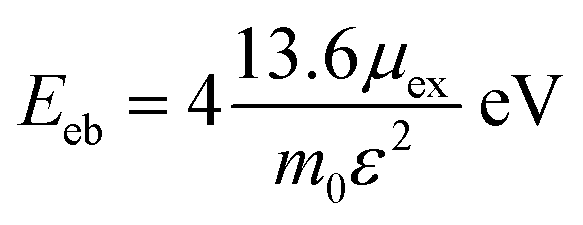 | (3) |
The optical absorption coefficients are obtained from dielectric function, as the followed equation represented:
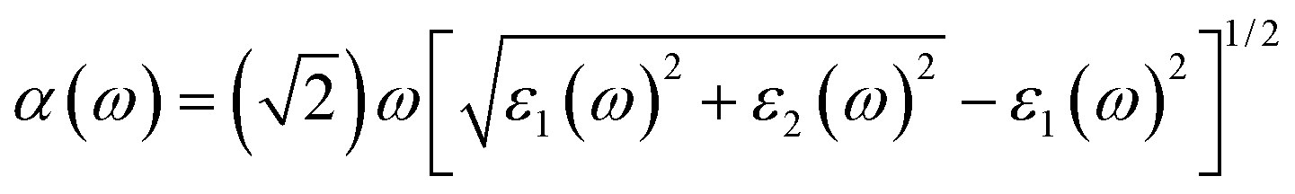 | (4) |
| ε(ω) = ε1(ω) + iε2(ω) | (5) |
Results and discussion
In recent years, 2D inorganic cubic phases of halide perovskites and 2D PtSe2 have been successfully synthesized, which attracted much attention due to the stability compared with 3D hybrid perovskite. The calculated lattice parameter of the monolayer cubic phase Cs2PbCl4, Cs2PbBr4, Cs2PbI4 is 5.64 Å, 5.91 Å, 6.30 Å, as listed in Table 1, which agree well with both experimental and theoretical values.42,43 Firstly, we chosen the (001) surface of Cs2PbX4 (X = Cl, Br, I) to construct the heterostructures, because it consists of alternating superposition of neutral planes [PbI2]0 and [CsI]0, which can effectively reduce dangling bonds.44,45 In addition, [CsI]0 interface exhibits stronger charge transferring than [PbI2]0, therefore Cs2PbX4–PtSe2 heterostructures consist of the [CsI]0 plane of the monolayer Cs2PbX4.42 In the Z direction, we use a large vacuum space of 20 Å to avoid the interlayer interaction. In order to find out the effect of halogen elements on Cs2PbX4–PtSe2 heterostructure, we firstly adopt the same heterostructure expansion method, as shown in Fig. S1.† The unit cells of 2D Cs2PbX4–PtSe2 are made up of supercell of monolayer PtSe2 and 2 × 2 supercell of monolayer Cs2PbX4. The optimized vertical interlayer distances of the Cs2PbCl4–PtSe2, Cs2PbBr4–PtSe2, Cs2PbI4–PtSe2 heterostructures calculated with vdW force are 2.76 Å, 2.79 Å, and 2.91 Å, which increase gradually with the halogen varying from Cl to I. However, the optimized vertical interlayer distances of Cs2PbX4–PtSe2 heterostructures calculated without vdW force are about 4 Å, so vdW force was considered in the optimization of Cs2PbX4–PtSe2 heterostructures.
| Heterostructures | Configuration | a (Å) | b (Å) | ΔZ (Å) | Mismatch (%) | Eb (meV) | Mismatch (%) | ||
|---|---|---|---|---|---|---|---|---|---|
| a = b (Å) | a = ba (Å) | a | b | ||||||
| a Values with PBE are from ref. 39. | |||||||||
| Cs2PbCl4–PtSe2 |  |
12.49 | 11.20 | 2.76 | 5.64 | 5.73 | −6.32 | 7.25 | 0.03 |
 |
18.37 | 13.18 | 2.84 | −7.78 | 2.68 | 3.66 | |||
| Cs2PbBr4–PtSe2 |  |
12.58 | 11.31 | 2.79 | 5.91 | 6.00 | −11.30 | 4.86 | 0.02 |
 |
18.55 | 13.34 | 2.89 | −46.07 | 0.30 | 1.27 | |||
| Cs2PbI4–PtSe2 |  |
12.86 | 11.33 | 2.91 | 6.30 | 6.40 | −16.78 | 1.66 | 5.26 |
 |
18.31 | 13.23 | 2.88 | −15.34 | 2.69 | 3.67 | |||
The interface binding energy (Eb) of Cs2PbCl4–PtSe2, Cs2PbBr4–PtSe2 and Cs2PbI4–PtSe2 interfaces is −6.32, −11.30 and −16.78 meV Å−2. The three Eb values are comparable to these of CsPbI3/MoS2 (−21 meV Å−2) and InSe/GaSe (−18.25 meV Å−2), suggesting that Cs2PbX4–PtSe2 heterostructures are stable in energy.46,47 With the halogen varying from Cl to I, the interface binding energies of Cs2PbX4–PtSe2 heterostructures decrease rapidly and heterostructures become more stable in energy due to the lower interface binding energy.48,49 Above all, the interlayer distance ranging from 2.76 Å to 2.91 Å belong to vdW and small interface binding energy revealed that 2D Cs2PbX4–PtSe2 heterostructures are formed by vdW contact. The lattice mismatches of the 2D Cs2PbCl4–PtSe2, Cs2PbBr4–PtSe2 and Cs2PbI4–PtSe2 heterostructures in the a and b directions are less than 7.25%, 4.86% and 5.54%.
The lattice mismatch between two layers is usually required to be less than 5% to ensure the stability of heterojunctions, the unit cell of Cs2PbX4–PtSe2 heterostructures are made up of  cubic phases Cs2PbCl4 and
  PtSe2,
  cubic phases Cs2PbBr4 and
  PtSe2, and
  cubic phases Cs2PbI4 and
  PtSe2, as shown in Fig. 1. The maximum lattice mismatches of the 2D Cs2PbCl4–PtSe2, Cs2PbBr4–PtSe2 and Cs2PbI4–PtSe2 heterostructures are 3.66%, 1.27% and 3.67%. The interface binding energy of Cs2PbCl4–PtSe2, Cs2PbBr4–PtSe2 and Cs2PbI4–PtSe2 interfaces is −7.78, −46.07 and −15.34 meV Å−2, respectively. By comparing the interface binding energy of the above six models, we find that the positive correlation between the lattice mismatch and interface binding energy. With the lattice mismatch decreases, the interface binding energy of heterostructures decreases. Cs2PbX4–PtSe2 heterostructures with smaller lattice mismatches are more stable due to the lower interface binding energy. Based on the stability, we chose the Cs2PbX4–PtSe2 heterostructures with smaller lattice mismatches to study their electronic properties and optical properties.
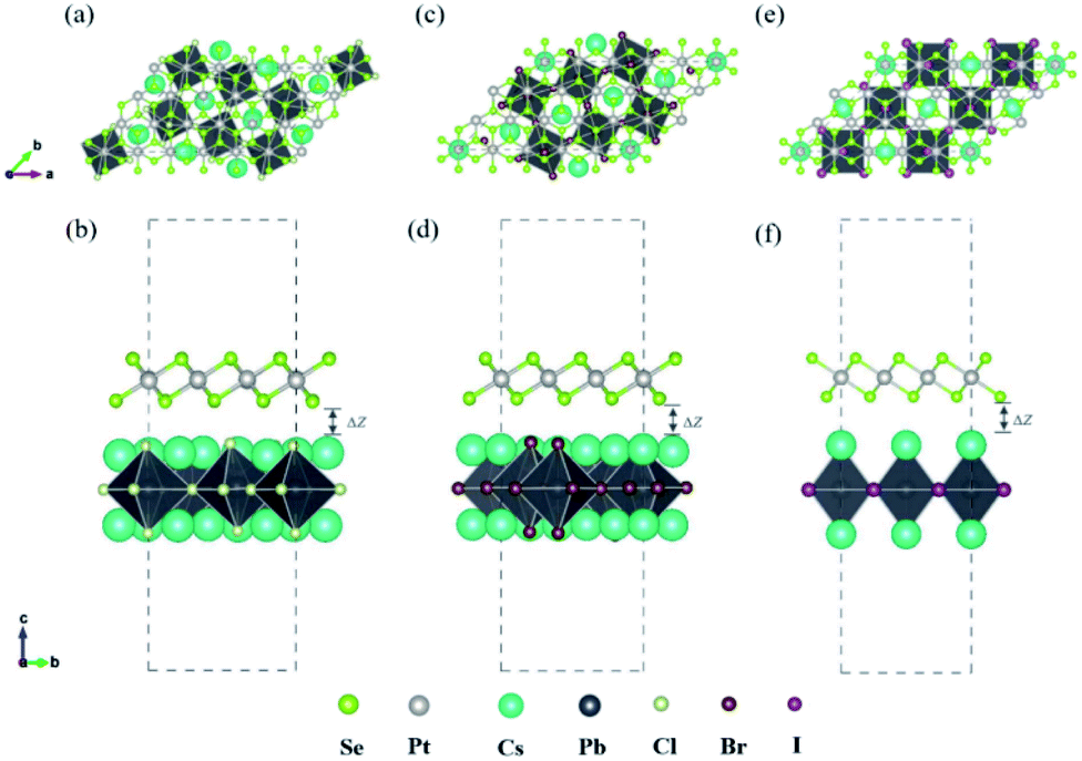 | ||
Fig. 1 Top and side views of relaxed 45° Cs2PbX4–PtSe2 heterostructures. (a and b) Cs2PbCl4–PtSe2 heterostructure. (c and d) Cs2PbBr4–PtSe2 heterostructure. (e and f) Cs2PbI4–PtSe2 heterostructure. The unit cell of Cs2PbX4–PtSe2 heterostructures are made up of  cubic phases Cs2PbCl4 and cubic phases Cs2PbCl4 and  PtSe2, PtSe2,  cubic phases Cs2PbBr4 and cubic phases Cs2PbBr4 and  PtSe2, and PtSe2, and  cubic phases Cs2PbI4 and cubic phases Cs2PbI4 and  PtSe2, as shown in figure. PtSe2, as shown in figure. | ||
To investigate the electronic properties and band alignments of 2D Cs2PbX4–PtSe2 heterostructures, we firstly studied electronic structures of the monolayer Cs2PbX4 and PtSe2. The band gaps of the monolayer Cs2PbX4 and PtSe2 are calculated by PBE, HSE, PBE with SOC (PBE + SOC) and HSE with SOC (HSE + SOC) functionals for comparison, the results are presented in Fig. S2 and Table S1.† It is shown that the band gaps calculated by HSE + SOC and PBE are very close to each other, while the band gap calculated by HSE is larger than PBE and the band gap calculated by PBE + SOC is smaller than PBE, which is consistent with earlier calculations on lead halide perovskites.50 The band gaps of monolayer Cs2PbCl4, Cs2PbBr4 and Cs2PbI4 by PBE functional are 2.59 eV, 2.18 eV and 1.84 eV, which are in good agreement with the theoretical and experimental band gaps of monolayer Cs2PbX4.7,10,14,51 In addition, the band gap of the PtSe2 monolayer using calculations PBE, HSE and HSE + SOC are 1.38 eV, 1.96 eV and 1.79 eV, respectively. Monolayer 1T-PtSe2 has an indirect bandgap of 1.2 eV measured experimentally with ARPES, which is more consistent with the PBE and PBE + SOC results.30,52 After comprehensive consideration, we apply PBE functional for further investigation.
Next, we calculated the electronic band structures of the Cs2PbX4–PtSe2 heterostructures by PBE functional, as shown in Fig. 2(a), (d) and (g). The conduction band minimum (CBM) of Cs2PbX4–PtSe2 heterostructures depends on PtSe2, while the valence band maximum (VBM) depends on PtSe2 for Cs2PbCl4–PtSe2 and Cs2PbI4–PtSe2 heterostructures and Cs2PbBr4 for Cs2PbBr4–PtSe2 heterostructure. The band edges of Cs2PbX4–PtSe2 heterojunctions are not equal to direct superposition of corresponding independent monolayer Cs2PbX4 and PtSe2, which are mainly induced by orbital coupling.53 The CBM consists of d-orbital PtSe2 and the VBM consists of p and d orbital of PtSe2 and Cs2PbX4, as shown in Fig. S3.† The Cs2PbCl4–PtSe2, Cs2PbBr4–PtSe2 and Cs2PbI4–PtSe2 heterostructures have an indirect bandgap with the value of 1.28 eV, 1.02 eV, and 1.29 eV, which approach optimal bandgap (1.34 eV) for solar cells.54
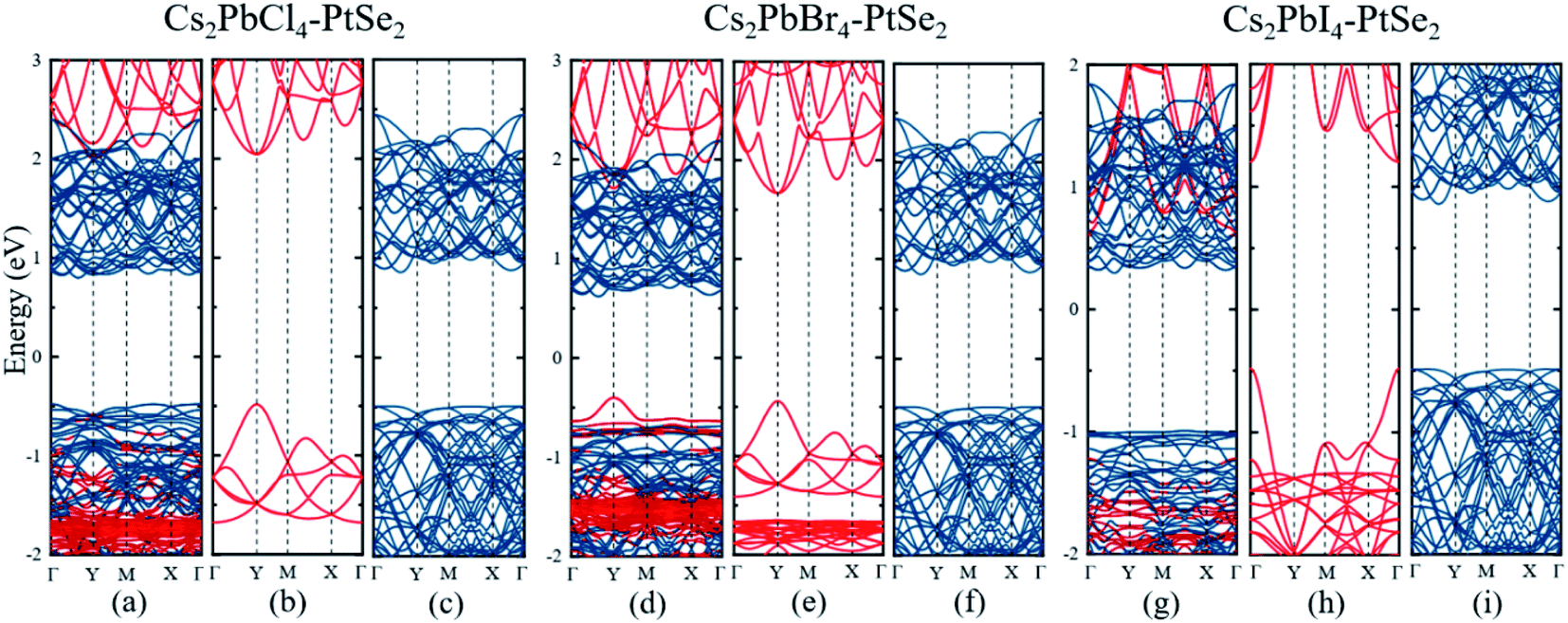 | ||
| Fig. 2 Electronic band structures of Cs2PbX4–PtSe2 heterostructures and corresponding monolayer Cs2PbX4 and PtSe2: (a–c) X = Cl; (d–f) X = Br; (g–i) X = I. The red and blue lines correspond to Cs2PbX4 and PtSe2, respectively. We calculated the electronic band structures of the Cs2PbX4–PtSe2 heterostructures by PBE functional. | ||
Furthermore, the Mott–Wannier theory has been used to approximate exciton binding energies in 2D.55 The carrier masses and MW exciton binding energy of Cs2PbX4–PtSe2 heterostructures are listed in Table 2. The lower carrier masses usually mean faster carrier transport.47 Therefore, Cs2PbBr4–PtSe2 heterostructure exhibit the highest hole and electron mobility among Cs2PbX4–PtSe2 heterostructures because it has the lowest me and mh. In addition, small exciton binding energy facilitates the splitting of excitons into free charge carriers, indicating that Cs2PbBr4–PtSe2 heterostructure can effectively promotes the separation of excitons.46 Therefore, Cs2PbBr4–PtSe2 heterostructure exhibits the highest charge transport efficiency among Cs2PbX4–PtSe2 heterostructures.
| Heterostructures | me (m0) | mh (m0) | μex (m0) | ε | Eeb (eV) |
|---|---|---|---|---|---|
| Cs2PbCl4–PtSe2 | 0.36 | 4.87 | 0.34 | 5.42 | 0.62 |
| Cs2PbBr4–PtSe2 | 0.34 | 0.44 | 0.19 | 5.55 | 0.34 |
| Cs2PbI4–PtSe2 | 0.38 | 4.88 | 0.35 | 5.86 | 0.56 |
In order to research energy level arrangement of Cs2PbX4–PtSe2 heterostructures, we explored energy band in monolayer Cs2PbX4 and PtSe2 from precontact (before contact) state to contact state. We set the vacuum level (Ev) to zero in the precontact state and set the Fermi level (Ef) to zero in the contact state to compare energy level heights of different heterostructures.56 In the precontact state, the CBM and VBM of monolayer Cs2PbX4 are both higher than that of monolayer PtSe2, as shown in Fig. 3(a). The electrons will diffuse from the Cs2PbX4 to the PtSe2 monolayer and the holes will move from the PtSe2 monolayer to the Cs2PbX4 monolayer when they contact. Correspondingly, the holes accumulate in Cs2PbX4 monolayer and the electrons accumulate in PtSe2 monolayer, leading to an increase of interface electric potential in Cs2PbX4 monolayer and a decrease of this in PtSe2 monolayer.48,49 Therefore, the band edges of Cs2PbX4 interface are bent upward and those of PtSe2 interface are bent downward after the contact of monolayer Cs2PbX4 and PtSe2. The difference between the Fermi level and the vacuum level is defined as the work function, representing the binding capacity of electrons.56 Calculated work functions of monolayers Cs2PbCl4, Cs2PbBr4, Cs2PbI4 and PtSe2 are 4.08 eV, 4.21 eV, 4.30 eV, and 5.29 eV, respectively. Therefore, the Fermi level of all Cs2PbX4 perovskites moved down and this of monolayer PtSe2 moved up after they contact each other, to keep the Fermi levels at the same level. The energy level diagram of Cs2PbX4–PtSe2 heterostructures in the contact is shown in Fig. 3(b). The Cs2PbBr4–PtSe2 heterostructure is type-II level alignment which is conducive to spontaneously drive the holes and electrons generated by the photoelectricity to move forward in opposite directions.48,49,57 However, the Cs2PbCl4–PtSe2 and Cs2PbI4–PtSe2 heterostructures are type-I level arrangement. Due to the type-II level alignment of Cs2PbBr4–PtSe2 heterostructure, it is useful to charge separation and improve PCE performance of Cs2PbX4 solar cells.
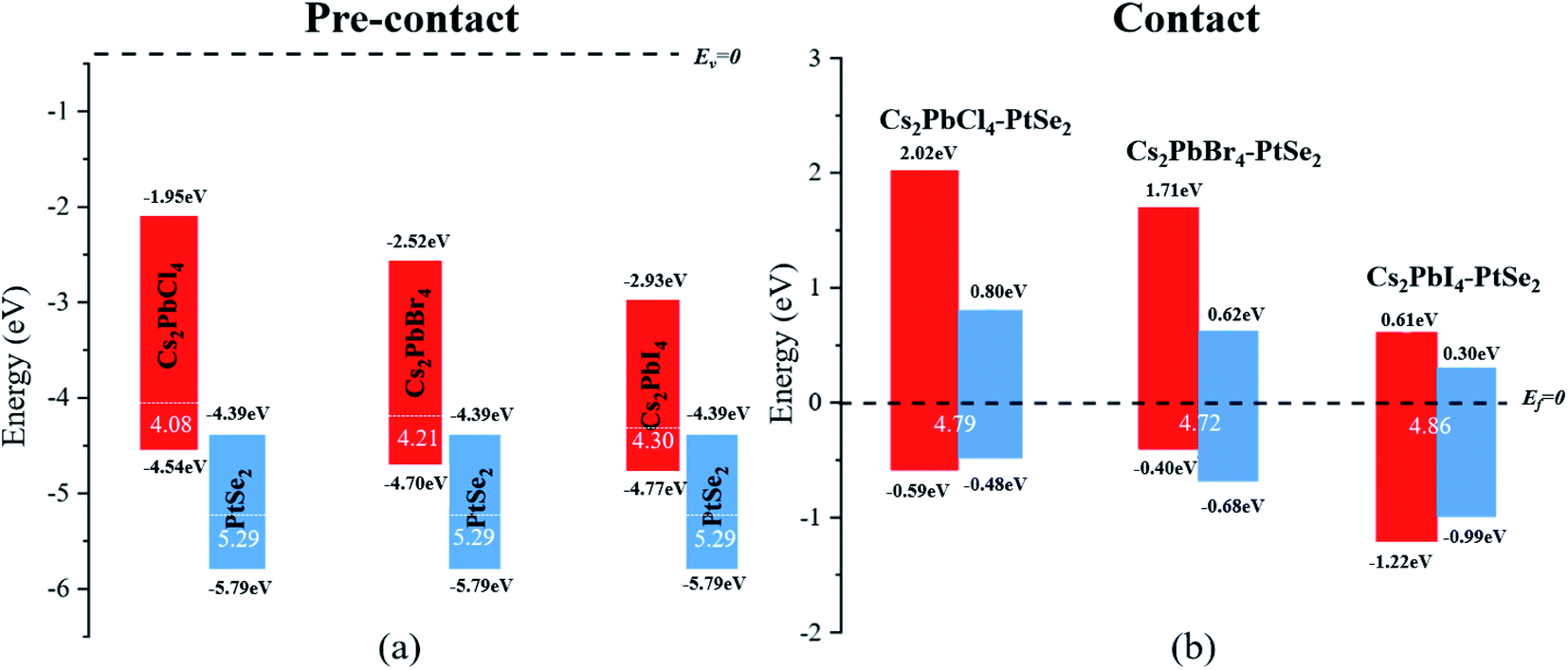 | ||
| Fig. 3 Energy level graphs of the monolayer PtSe2 and Cs2PbX4 in the (a) precontact and (b) contact. Red and blue rectangles represent the monolayer Cs2PbX4 and PtSe2. The bottom and top of rectangles correspond to VBM and CBM, respectively. The work function is labeled in the rectangles. In order to research energy level arrangement of Cs2PbX4–PtSe2 heterostructures, we explored energy band in monolayer Cs2PbX4 and PtSe2 from precontact (before contact) state to contact state. | ||
In order to research the interfacial contact and charge transfer mechanism of Cs2PbX4–PtSe2 heterostructures, plane-averaged charge density difference and corresponding 3D charge density difference were computed, as shown in Fig. 4. It is shown that electrons accumulate in PtSe2 layer which is represented by blue region and the electrons dissipate in Cs2PbX4 interface represented by red region, indicating that the electrons transfer from Cs2PbX4 monolayer to the PtSe2 monolayer. In addition, the holes primarily accumulate in the Cs2PbX4 interface, revealing that the holes transfer from PtSe2 monolayer to the Cs2PbX4 monolayer. Besides, the amounts of the charge transferring in the Cs2PbX4–PtSe2 heterostructures follow the order Cl < Br < I, indicating Cs2PbI4–PtSe2 and Cs2PbBr4–PtSe2 heterostructures are more beneficial to interfacial charge transfer.
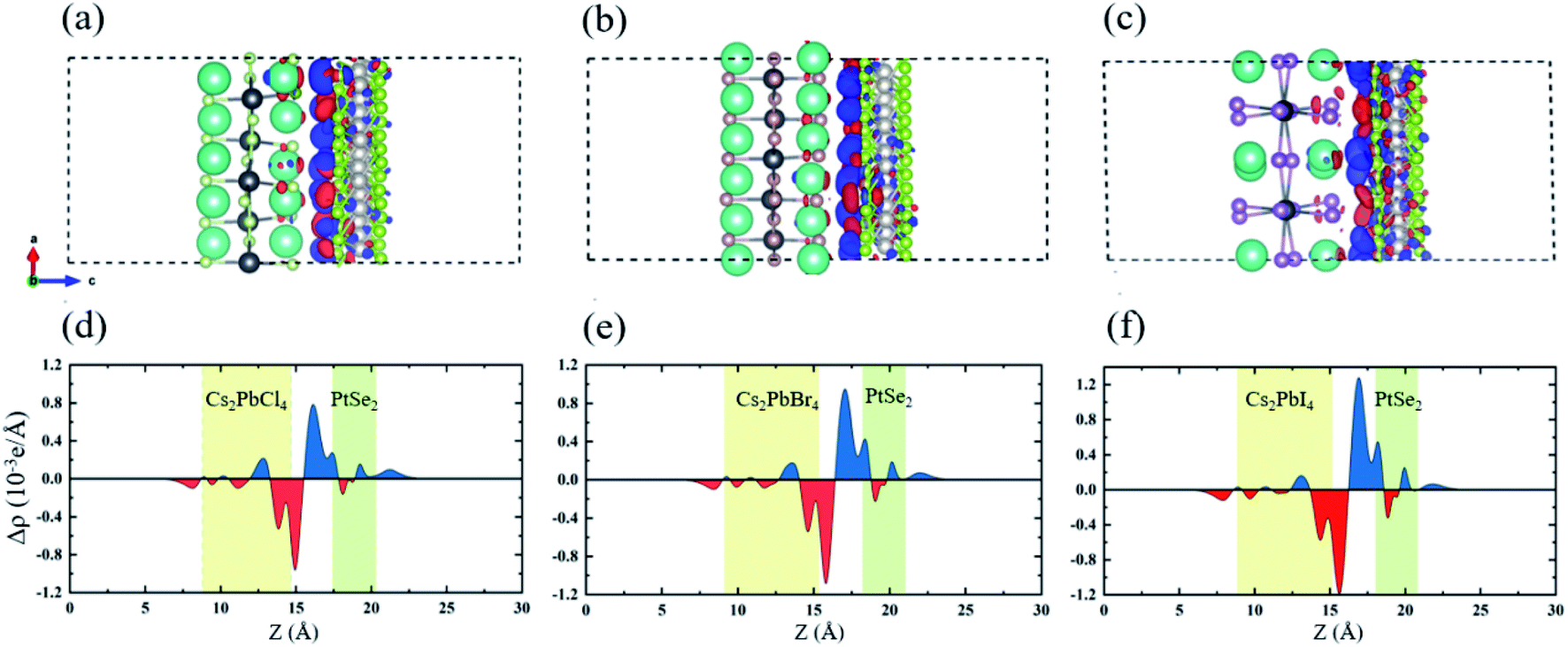 | ||
| Fig. 4 3D charge density difference and corresponding planar-averaged differential charge density Δρ(z) of Cs2PbX4–PtSe2 heterostructures: (a and d) X = Cl; (b and e) X = Br; (c and f) X = I. Red and blue represent electron depletion and accumulation. The yellow and green areas represent Cs2PbX4 and PtSe2, respectively. In order to research the interfacial contact and charge transfer mechanism of Cs2PbX4–PtSe2 heterostructures, Plane-averaged charge density difference and corresponding 3D charge density difference were computed. | ||
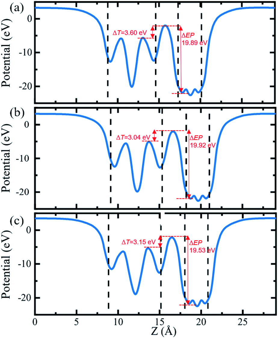
In order to further compare the charge transfers of the three heterojunctions, the plane-averaged electrostatic potentials of 2D Cs2PbX4–PtSe2 heterostructures in the z direction are presented in Fig. 5. The electrostatic potentials drop from perovskites monolayer to PtSe2 monolayer in the interfaces. The electrostatic potential difference values (ΔEP, marked in Fig. 5) are involved in the charge transfers. A larger ΔEP implies a powerful built-in electrostatic field which could lead to carrier dynamics and charge transfer.47,48 The ΔEP of Cs2PbCl4–PtSe2, Cs2PbBr4–PtSe2 and Cs2PbI4–PtSe2 heterostructures are 19.89 eV, 19.92 eV and 19.53 eV, respectively. Therefore, the Cs2PbBr4–PtSe2 heterostructure has the highest charge transfers in the three Cs2PbX4–PtSe2 heterostructures due to the highest ΔEP. In addition, tunnel barrier height (ΔT, marked in Fig. 6.) determines the electron transport efficiency, when the ΔT is lower, the charge injection efficiency is higher.47 The ΔT of Cs2PbCl4–PtSe2, Cs2PbBr4–PtSe2 and Cs2PbI4–PtSe2 heterostructures is 3.60 eV, 3.04 eV and 3.15 eV, respectively. Tunnel barrier height of Cs2PbBr4–PtSe2 heterostructure is the lowest in the three Cs2PbX4–PtSe2 heterostructures, so Cs2PbBr4–PtSe2 heterostructure has the highest charge transport efficiency. From the above, Cs2PbBr4–PtSe2 heterostructure has great potential for optoelectronic applications due to the highest ΔEP and the lowest ΔT.
 | ||
| Fig. 5 The planar-averaged electrostatic potentials of Cs2PbX4–PtSe2 eterostructures. (a) Cs2PbCl4–PtSe2 heterostructure, (b) Cs2PbBr4–PtSe2 heterostructure, (c) Cs2PbI4–PtSe2 heterostructure. In order to further compare the charge transfers of the three heterojunctions, the plane-averaged electrostatic potentials of 2D Cs2PbX4–PtSe2 heterostructures in the z direction are presented in figure. | ||
 | ||
| Fig. 6 The planar-averaged electrostatic potentials of Cs2PbX4–PtSe2 heterostructures. (a) Cs2PbCl4–PtSe2 heterostructure, (b) Cs2PbBr4–PtSe2 heterostructure, (c) Cs2PbI4–PtSe2 heterostructure. The optical properties of perovskites have an important influence on the perovskite optoelectronic devices besides electronic structure. | ||
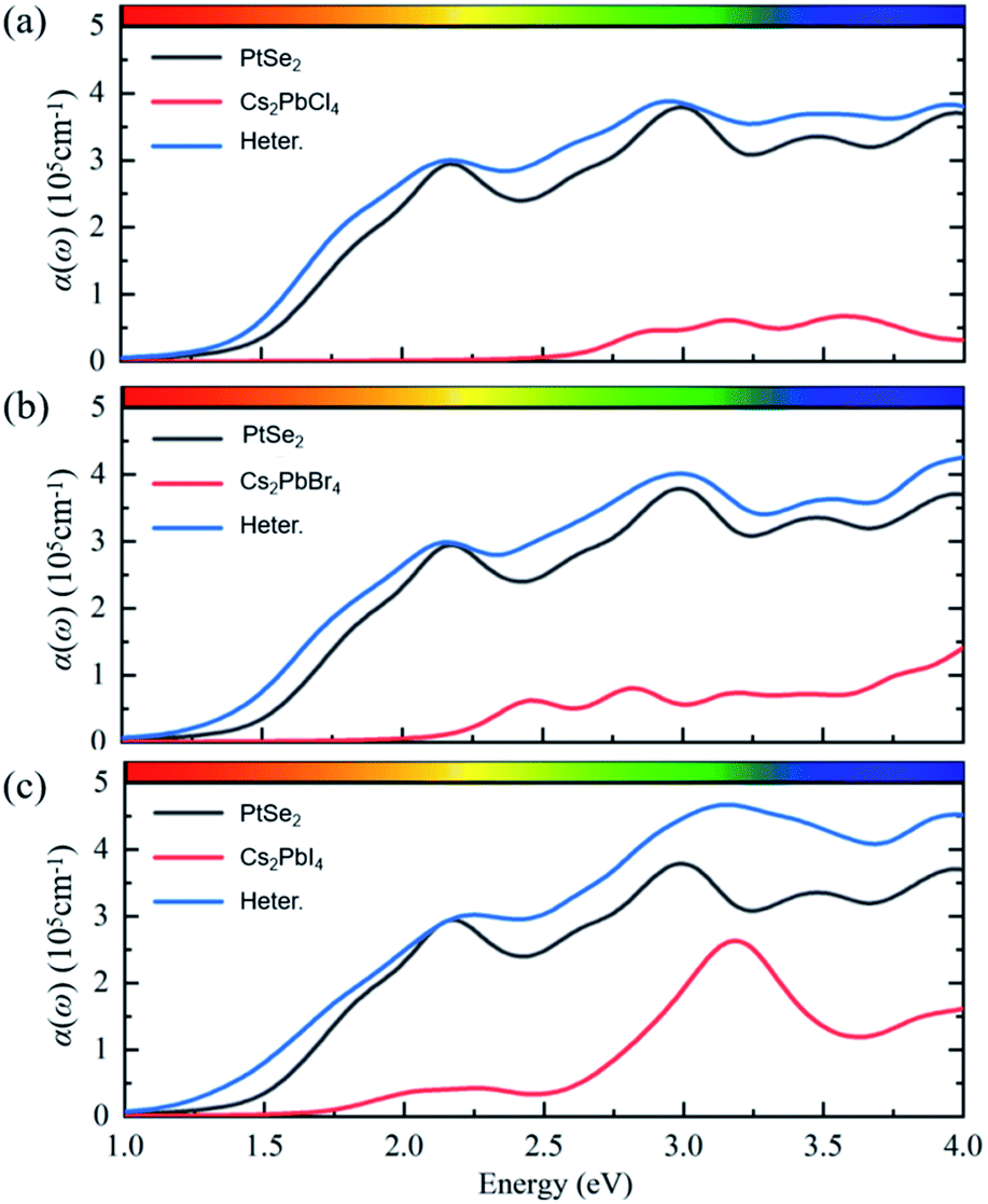
The optical properties of perovskites have an important influence on the perovskite optoelectronic devices besides electronic structure. The optical absorption coefficients of single-layer PtSe2, single-layer Cs2PbX4, and corresponding heterostructures were calculated, as represented in Fig. 6. The optical absorptions of all heterostructures are significantly greater than the corresponding monolayer Cs2PbX4 and PtSe2, which could be related to the interface contact of heterostructures. The light absorption coefficient of Cs2PbX4–MSe2 heterostructures is at least twice higher than that of monolayer 2D inorganic halide perovskites. With the halogen varying from Cl to I, the light absorption coefficients of the Cs2PbX4–PtSe2 heterostructures increase rapidly in the visible region. In the visible region, optical absorption spectra of Cs2PbI4 is highest in the Cs2PbX4 perovskites and the optical absorption spectra of Cs2PbCl4 is lowest in the Cs2PbX4 perovskites. The Cs2PbI4–PtSe2 heterostructure shows the maximum optical absorption in visible regions. In addition, the optical absorption coefficients of single-layer PtSe2 are larger than those of 2D inorganic Cs2PbX4 perovskites in the visible and ultraviolet regions. Therefore, building PtSe2 and 2D inorganic halide perovskite heterostructures would be an effective way to improve the optical absorption of 2D inorganic halide perovskite.
Conclusions
In conclusion, we studied the structural, stability, optoelectronic properties and charge transfer mechanism of 2D halide perovskite heterostructures Cs2PbX4–PtSe2 (X = Cl, Br, I). Our results represent that 2D Cs2PbX4–PtSe2 heterostructures are formed by van der Waals contact. Cs2PbCl4–PtSe2, Cs2PbBr4–PtSe2 and Cs2PbI4–PtSe2 heterostructures have an indirect bandgap with the value of 1.28 eV, 1.02 eV, and 1.29 eV, respectively, which approach optimal bandgap (1.34 eV) for solar cells. In the precontact state, all the Cs2PbX4–PtSe2 heterostructures exhibit type-II band arrangement, which drives the spontaneous motion of the carrier. In the contact state, Cs2PbBr4–PtSe2 exhibits type-II band arrangement, while heterojunctions Cs2PbCl4–PtSe2 and Cs2PbI4–PtSe2 exhibit type-I band alignment. The charge density difference confirms that the holes transfer from PtSe2 monolayer to the Cs2PbX4 monolayer and the electrons transfer from Cs2PbX4 monolayer to PtSe2 monolayer. Furthermore, the Cs2PbBr4–PtSe2 heterostructure has the highest electron transport efficiency due to the highest ΔEP and the lowest ΔT. In addition, the light absorption coefficient of Cs2PbX4–MSe2 heterostructures is at least twice higher than that of monolayer 2D inorganic halide perovskites. In summary, the construction of 2D inorganic halide perovskites and monolayer PtSe2 heterostructures is a useful method to enhance the optoelectronic performance of 2D inorganic halide perovskites for optoelectronic and photovoltaic applications.Conflicts of interest
There are no conflicts to declare.Acknowledgements
This work is supported by the Fund of State Key Laboratory of IPOC(BUPT) (No. IPOC2019ZZ04) and the Open-Foundation of Key Laboratory of Laser Device Technology, China North Industries Group Corporation Limited (Grant No. KLLDT202103). We thank for the helpful discussion with Prof. Pengfei Guan and the computational support from the Beijing Computational Science Research Center (CSRC).Notes and references
- A. T. Barrows, A. J. Pearson, C. K. Kwak, A. D. F. Dunbar, A. R. Buckley and D. G. Lidzey, Energy Environ. Sci., 2014, 7, 2944–2950 RSC.
- Y.-H. Kim, G.-H. Lee, Y.-T. Kim, C. Wolf, H. J. Yun, W. Kwon, C. G. Park and T. W. Lee, Nano Energy, 2017, 38, 51–58 CrossRef CAS.
- J. Lu, A. Carvalho, H. Liu, S. X. Lim, A. H. Castro Neto and C. H. Sow, Angew. Chem., Int. Ed., 2016, 55, 11945–11949 CrossRef CAS PubMed.
- A. Kojima, K. Teshima, Y. Shirai and T. Miyasaka, J. Am. Chem. Soc., 2009, 131, 6050–6051 CrossRef CAS PubMed.
- K. Xiao, R. Lin, Q. Han, Y. Hou, Z. Qin, H. T. Nguyen, J. Wen, M. Wei, V. Yeddu, M. I. Saidaminov, Y. Gao, X. Luo, Y. Wang, H. Gao, C. Zhang, J. Xu, J. Zhu, E. H. Sargent and H. Tan, Nat. Energy, 2020, 5, 870–880 CrossRef CAS.
- J. H. Noh, S. H. Im, J. H. Heo, T. N. Mandal and S. I. Seok, Nano Lett., 2013, 13, 1764–1769 CrossRef CAS PubMed.
- P. B. Gui, H. Zhou, F. Yao, Z. H. Song, B. R. Li and G. J. Fang, Small, 2019, 15 DOI:10.1002/smll.201902618.
- H. Feng, C. C. Stoumpos, P. Guo, N. Zhou, T. J. Marks, R. P. H Chang and M. G. Kanatzidis, J. Am. Chem. Soc., 2015, 137, 11445–11452 CrossRef PubMed.
- L. Wu, P. Lu, Y. Li, Y. Sun, J. Wong and K. Yang, J. Mater. Chem. A, 2018, 6, 24389–24396 RSC.
- Y. H. Li and K. S. Yang, Energy Environ. Sci., 2019, 12, 2233–2243 RSC.
- Y. Li, D. Maldonado-Lopez, V. R. Vargas, J. Zhang and K. Yang, J. Chem. Phys., 2020, 152, 084106 CrossRef CAS PubMed.
- S. Chen and G. Shi, Adv. Mater., 2017, 29 DOI:10.1002/adma.201605448.
- A. Bala, A. K. Deb and V. Kumar, J. Phys. Chem. C, 2018, 122, 7464–7473 CrossRef CAS.
- J. Song, L. Xu, J. Li, J. Xue, Y. Dong, X. Li and H. Zeng, Adv. Mater., 2016, 28, 4861–4869 CrossRef CAS PubMed.
- J. C. Liu, S. Lin, K. Huang, C. Jia, Q. M. Wang, Z. W. Li, J. N. Song, Z. L. Liu, H. Y. Wang, M. Lei and H. Wu, npj Flexible Electron., 2020, 4, 10 CrossRef CAS.
- K. Bi, Q. M. Wang, J. C. Xu, L. H. Chen, C. W. Lan and M. Lei, Adv. Opt. Mater., 2021, 9, 2001474 CrossRef CAS.
- J. C. Xu, K. Bi, R. Zhang, Y. N. Hao, C. W. Lan, M.-M. Klaus, X. J. Zhai, Z. D. Zhang and S. G. H, Research, 2019, 2019, 968621 Search PubMed.
- S. Lin, J. C. Liu, W. Z. Li, D. Wang, Y. Huang, C. Jia, Z. W. Li, H. Y. Wang, J. N. Song, Z. L. Liu, K. Huang, D. Zu, M. Lei, B. Hong and H. Wu, Nano Lett., 2019, 19, 6853–6861 CrossRef CAS PubMed.
- J. C. Xu, J. Q. Cao, M. H. Guo, S. L. Yang, H. M. Yao, M. Lei, Y. N. Hao and K. Bi, Adv. Compos. Hybrid Mater., 2021, 4, 761–767 CrossRef.
- Q. M. Wang, J. M. Zhang, Z. D. Zhang, Y. N. Hao and K. Bi, Adv. Compos. Hybrid Mater., 2020, 3, 58–65 CrossRef CAS.
- B. N. Jia, P. F. Zhu, S. H. Sun, L. H. Han, G. Liu, Y. Wang, G. D. Peng and P. F. Lu, J. Sichuan Norm. Univ., Nat. Sci., 2020, 26, 1–6 Search PubMed.
- X. Song, X. Liu, D. Yu, C. Huo, J. Ji, X. Li, S. Zhang, Y. Zou, G. Zhu, Y. Wang, M. Wu, A. Xie and H. Zeng, ACS Appl. Mater. Interfaces, 2018, 10, 2801–2809 CrossRef CAS PubMed.
- D. Wijethunge, L. Zhang, C. Tang and A. Du, Front. Phys., 2020, 15, 63504 CrossRef.
- X. R. Hu, J. M. Zheng and Z. Y. Ren, Front. Phys., 2018, 13, 137302 CrossRef.
- Z. P. Zhou, M. A. Springer, W. X. Geng, X. Y. Zhu, T. C. Li, M. M. Li, Y. Jing and T. Heine, J. Phys. Chem. Lett., 2021, 12, 8134–8140 CrossRef CAS PubMed.
- Y. Jing, Z. P. Zhou, W. X. Geng, X. Y. Zhu and T. Heine, Adv. Mater., 2021, 33, 2008645 CrossRef CAS PubMed.
- Y. Jing, Z. P. Zhou, J. Zhang, C. B. Huang, Y. F. Li and F. Wang, Phys. Chem. Chem. Phys., 2019, 21, 21064–21069 RSC.
- Y. Choi, S. Jung, N. K. Oh, J. Lee, J. Seo, U. Kim, D. Koo and H. Park, Chemnanomat, 2019, 5, 1050–1058 CrossRef CAS.
- Y. Wang, L. Li, W. Yao, S. Song, J. T. Sun, J. Pan, X. Ren, C. Li, E. Okunishi, Y.-Q. Wang, E. Wang, Y. Shao, Y. Y. Zhang, H.-t. Yang, E. F. Schwier, H. Iwasawa, K. Shimada, M. Taniguchi, Z. Cheng, S. Zhou, S. Du, S. J. Pennycook, S. T. Pantelides and H.-J. Gao, Nano Lett., 2015, 15, 4013–4018 CrossRef CAS PubMed.
- R. A. B. Villaos, C. P. Crisostomo, Z.-Q. Huang, S.-M. Huang, A. A. B. Padama, M. A. Albao, H. Lin and F.-C. Chuang, npj 2D Mater. Appl., 2019, 3 DOI:10.1038/s41699-018-0085-z.
- Y. Zhao, J. Qiao, Z. Yu, P. Yu, K. Xu, S. P. Lau, W. Zhou, Z. Liu, X. Wang, W. Ji and Y. Chai, Adv. Mater., 2017, 29 DOI:10.1002/adma.201604230.
- A. Ciarrocchi, A. Avsar, D. Ovchinnikov and A. Kis, Nat. Commun., 2018, 9 DOI:10.1038/s41467-018-03436-0.
- L.-H. Zeng, S.-H. Lin, Z.-J. Li, Z.-X. Zhang, T.-F. Zhang, C. Xie, C.-H. Mak, Y. Chai, S. P. Lau, L.-B. Luo and Y. H. Tsang, Adv. Funct. Mater., 2018, 28 DOI:10.1002/adfm.201705970.
- Z. X. Zhang, L. H. Zeng, X. W. Tong, Y. Gao, C. Xie, Y. H. Tsang, L. B. Luo and Y. C. Wu, J. Phys. Chem. Lett., 2018, 9, 1185–1194 CrossRef CAS PubMed.
- P. E. Blochl, Phys. Rev. B: Condens. Matter Mater. Phys., 1994, 50, 17953–17979 CrossRef PubMed.
- G. Kresse and D. Joubert, Phys. Rev. B: Condens. Matter Mater. Phys., 1999, 59, 1758–1775 CrossRef CAS.
- J. P. Perdew, K. Burke and M. Ernzerhof, Phys. Rev. Lett., 1996, 77, 3865–3868 CrossRef CAS PubMed.
- X. N. Guan, R. Zhang, B. N. Jia, L. Y. Wu, B. Zhou, L. Fan, G. Liu, Y. Wang, P. F. Lu and G. D. Peng, J. Non-Cryst. Solids, 2020, 550, 120388 CrossRef CAS.
- B. Liu, M. Long, M.-Q. Cai and J. Yang, Appl. Phys. Lett., 2018, 112, 043901 CrossRef.
- J. Heyd, G. E. Scuseria and M. Ernzerhof, J. Chem. Phys., 2003, 118, 8207–8215 CrossRef CAS.
- P. Z. B. Jia, S. Sun, L. Han, G. Liu, Y. Wang, G.-D. Peng and P. Lu, IEEE J. Sel. Top. Quantum Electron., 2019, 26, 1–6 Search PubMed.
- A. Molina-Sanchez, ACS Appl. Energy Mater., 2018, 1, 6361–6367 CrossRef.
- J.-H. Yang, Q. Yuan and B. I. Yakobson, J. Phys. Chem. C, 2016, 120, 24682–24687 CrossRef CAS.
- J. Haruyama, K. Sodeyama, L. Han and Y. Tateyama, J. Phys. Chem. Lett., 2014, 5, 2903–2909 CrossRef CAS PubMed.
- D.-J. Yang, Y.-H. Du, Y.-Q. Zhao, Z.-L. Yu and M.-Q. Cai, Phys. Status Solidi B, 2019, 256 DOI:10.1002/pssb.201800540.
- J. H. Chen, X. J. He, B. S. Sa, J. Zhou, C. Xu, C. L. Wen and Z. M. Sun, Nanoscale, 2019, 11, 6431–6444 RSC.
- J. He, J. Su, Z. Lin, S. Zhang, Y. Qin, J. Zhang, J. Chang and Y. Hao, J. Phys. Chem. C, 2019, 123, 7158–7165 CrossRef CAS.
- Y.-Q. Zhao, Y. Xu, D.-F. Zou, J.-N. Wang, G.-F. Xie, B. Liu, M.-Q. Cai and S.-L. Jiang, J. Phys.: Condens. Matter, 2020, 32, 19 CAS.
- B. Liu, M. Long, M.-Q. Cai and J. Yang, J. Phys. Chem. Lett., 2018, 9, 4822–4827 CrossRef CAS PubMed.
- W. J. Yin, J. H. Yang, J. Kang, Y. Yan and S. H. Wei, J. Mater. Chem. A, 2015, 3, 8926–8942 RSC.
- P. B. Gui, H. Zhou, F. Yao, Z. H. Song, B. R. Li and G. J. Fang, Small, 2019, 15 DOI:10.1002/adom.201800879.
- L. Fang, W. Liang, Q. Feng and S.-N. Luo, J. Phys.: Condens. Matter, 2019, 31, 455001 CrossRef CAS PubMed.
- Y. Si, H. Y. Wu, K. Yang, J. C. Lian, T. Huang, W. Q. Huang, W. Y. Hu and G. F. Huang, Appl. Phys. Lett., 2021, 119, 043102 CrossRef CAS.
- S. Ruhle, Sol. Energy, 2016, 130, 139–147 CrossRef.
- P. Wang, Y. X. Zong, H. Liu, H. Y. Wen, H. X. Deng, Z. M. Wei, H. B. Wu and J. B. Xia, J. Phys. Chem. C, 2020, 214, 23832–23838 CrossRef.
- B. Liu, Y.-Q. Zhao, Z.-L. Yu, L.-Z. Wang and M.-Q. Cai, J. Colloid Interface Sci., 2018, 513, 677–683 CrossRef CAS PubMed.
- W. Niu, A. Eiden, G. V. Prakash and J. J. Baumberg, Appl. Phys. Lett., 2014, 104, 171111 CrossRef.
Footnote |
| † Electronic supplementary information (ESI) available: The band structures of monolayer Cs2PbX4 and PtSe2 by different calculation functional. See DOI: 10.1039/d1ra08574c |
| This journal is © The Royal Society of Chemistry 2022 |