DOI:
10.1039/D1RA08154C
(Paper)
RSC Adv., 2022,
12, 3745-3754
Potential outstanding physical properties of novel black arsenic phosphorus As0.25P0.75/As0.75P0.25 phases: a first-principles investigation
Received
7th November 2021
, Accepted 24th January 2022
First published on 28th January 2022
Abstract
Black arsenic phosphorus As0.5P0.5 has been studied as an excellent candidate for electronic and optoelectronic applications. At the same time, the physical properties of AsxP1−x alloys with other compositions were not investigated. In this work, we design seven As0.25P0.75(P-I and P-II)/As0.75P0.25(As-(I, II, III, IV and V)) phases with molecular dynamics stability. First principles calculations are used to study their electronic structures under strain as well as their carrier mobilities. By calculating Perdew–Burke–Ernzerhof (PBE) electronic bands, we reveal that these materials are direct-gap semiconductors similar to black phosphorus except for the As-IV phase. It is also found that the carrier mobility in the P-I and As-V phases can reach 104 cm2 V−1 s−1. The electronic structures of the P-I, As-IV and As-V phases under strain are studied. Finally, we design caloritronic devices based on armchair and zigzag nanoribbons. The value of the Seebeck coefficient of the armchair and zigzag devices made from the P-II phases are found to be as high as 2507 and 2005 μW K−1 at 300 K. The thermal properties of the arsenic phosphorus phases under consideration are further studied by calculating their thermoelectric figure of merit, ZT values. These values are as high as 10.88 for the armchair devices based on the As-III phase and 4.59 for the zigzag devices based on the As-V phase at room temperature, and 15 and 7.16 at 600 K, respectively. The obtained results demonstrate that the As0.25P0.75/As0.75P0.25 phases studied here can be regarded as potential candidates for thermoelectric and electronic device applications.
I. Introduction
For practical applications, semiconductors of the first- and second-generation such as Si1,2 and SiC3 have been widely used. However, the dimensions of devices based on these semiconductors have already reached their minimum limit. Moreover, a number of physical properties of these materials can no longer meet the actual practical needs. In this respect, third-generation semiconductors such as GaAs and GaO are widely studied for device applications.4 As compared to Si, they have higher thermal conductivities, breakdown field strength and saturation.5 Looking further to the future, theoretical materials science is challenged by the search for and design of new semiconductor materials with ever increasing performance as compared to traditional semiconductors.
The two-dimensional material graphene6 has attracted great attention since its discovery due to its excellent electrical, optical and mechanical properties. Graphene is characterized by a high carrier mobility because of the massless Fermi–Dirac structure. However, being a unique zero-bandgap semiconductor material, it has limited electrical applications. Therefore, searching for new two-dimensional materials with suitable electrical properties and large bandgap values has become one of the mainstreams in semiconductor field. This road leads from the van der Waals heterogeneous (vdwh) structural materials, such as h-BN.7,8 BN has a similar honeycomb structure to that of graphene and the same excellent performance in certain aspects, to the combination of vdwh material with graphene, which enable open its band gap of graphene;9–14 to the, MXene,15 which are excellent materials for solar cell and catalysis applications; to the monolayer materials such as CdTe, MoS2 (ref. 16) and a number of others, and to the currently popular phosphorene and arsenene.16–20
The popularity of phosphorene for researchers has recently increased because of its high carrier mobility and large direct band gap.21 However, due to the instability of P–P bonds, the structure of phosphorene is poorly stable and degrades under atmospheric influences. Such property hinders device applications of this material. It is found later that the alloying phosphorene with arsenic (AsxP1−x),22 which is also a fifth main group element, enables to achieve more stable structure keeping the same excellent properties of phosphorene. In addition, by changing the alloy composition, tuning its bandgap become possible. Up to now, five stable As0.5P0.5 phases are found to be stable, including α-phase (black arsenic phosphorus),23 β-phase (blue phosphorus) and θ-phase. Among these, the α phase has relatively superior performance. In the studies on As0.5P0.5 phase study,24 a calculated HSE06 energy band structure with a band gap of 1.47 eV and a carrier mobility of 104 cm2 V−1 s−1 are revealed for the α3 phase.25 Sun et al. investigated the electrical structure of one phase of As0.33P0.67 and As0.67P0.33.37 However, electronic structures of phosphorene-arsenic alloys different from the reported above compositions are not investigated in detail, existence of other phases with better excellent electrical and thermal properties as compared to those of studied materials cannot be excluded.
In this paper, we performed simulations of all the phases of black arsenic phosphorus with As0.75P0.25 and As0.25P0.75 compositions. In particular, we focus on the electrical and thermal properties of seven phases that are stable in molecular dynamics simulations. For the study of electrical properties, the energy band structures of the phases under consideration are first calculated by PBE method, The calculated band structures are found similar to the one of α3 phase. Supposing that these phases might also have very high carrier mobilities, the latter are calculated. The flexibility of the phases under study is investigated by applying a −10–8% biaxial and uniaxial strain. A higher flexibility for the P-I phase is established, which is a further evidence of higher carrier mobility. We also find that the As-V phase undergoes a of semiconductor–metal–semiconductor transition under uniaxial strain along the armchair direction. In order to explain this phenomenon, the electronic orbital interactions resulted from strain application is analyzed. Recently, Kolos et al. found that mixed V group electron-based materials can exhibit strong exciton effects and the properties can be temperature-dependent.36 So, we focus on the effect of temperature on the thermal properties of the devices made up of these phases. Finally, we estimate thermoelectric properties of the phases considered by designing them as simple one-dimensional devices and calculating their Seebeck coefficients and thermoelectric preferences.
II. Computational methods
The calculations were performed using the Vienna Ab initio Simulation Package (VASP)26,27 and Virtual NanoLab & Atomistix ToolKit (VNL-ATK) based on density generalized functional theory (DFT). To describe the electron-ion and electron–electron exchange correlation interactions,28 the projector augmented wave (PAW)29 method and the generalized gradient approximation (GGA)30 function were used, respectively. The phonon scattering calculations were performed using a super-monolithic finite method shift implemented in the PHONOPY package31 and using VASP as a force constant calculator. A simplified k-points sampling grid of 6 × 6 × 1 points on a 6 × 6 × 1 supercell was used for force evaluation. For structure optimization and electronic structure calculations, the Brillouin zone of As0.75P0.25 and As0.25P0.75 primitive were gridded with 16 × 16 × 1 k-points. The crystal structures of the different phases were optimized with a plane wave energy cutoff of 400 eV and a strict convergence criterion (0.01 eV Å−1). Vacuum layer 15 Å to avoid lattice periodicity of atoms. In this paper, the hybrid generalized (HSE06)32,33 method was also used to correct the known band gap estimates in the PBE calculations.
In two-dimensional materials, the coherence wavelength of thermally activated electrons or holes at room temperature is much longer than the lattice constant, close to the acoustic phonon wavelength, and can be obtained according to the theory of the Badin and Shockley transformation situation (DP) first obtained by starting from the electron–phonon coupling in the longitudinal phonon limit, the carrier mobility expression is as follows:34
here

is the effective mass in the transport direction and
md is the average effective mass determined by

.
T is the temperature and
C2D is the elastic modulus of uniform deformation of
x (zigzag) and
y (armchair) used to model the lattice distortion caused by strain. In the two-dimensional system,
C2D can be defined as
C2D = [∂
2E/∂
2δ2]/
S0; here
E is the total energy of the supercell, which is the applied uniaxial strain, and
S0 is the area of the supercell in equilibrium;
Ei is the DP constant which characterizes the band edge shift caused by strain and can be defined as
Ei = Δ
Eli/(Δ
l/
l0).
III. Results and discussion
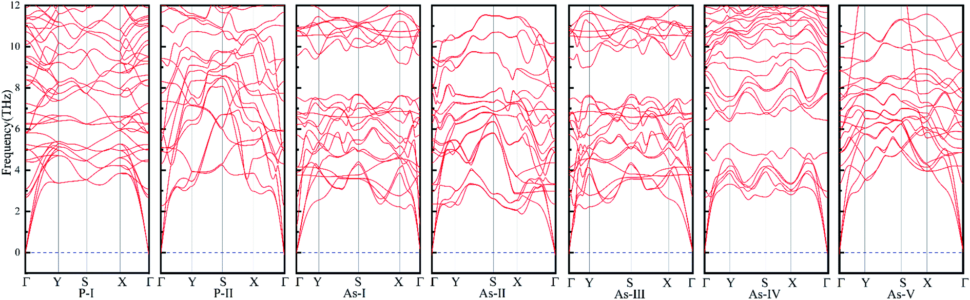
We have designed thirty possible As0.75P0.25 and As0.25P0.75 phases, seven of which can be demonstrated to be stably by dynamics calculations, and the schematic structures of the seven phases are shown in Fig. 1. Fig. 1(a)–(h) show their top and side views, among them Fig. 1(a) and (b) show two phases of As0.25P0.75 and Fig. 1(c)–(g) show the other five phases of As0.75P0.25, which are named according to our study order for the convenience of representation in this paper. Fig. 2 shows the calculated phonon spectra corresponding to these seven phases, and it is obvious that the phonon spectra corresponding to them are almost free of imaginary frequencies, which proves their molecular dynamics stability. In order to compare the geometry property of these phases more clearly, Table 1 shows the geometric parameters of these phases, where the in-plane/out-plane bond and the in-plane/out-plane angle ψ determine the length of the structure along the zigzag/armchair direction, the longer the in-plane bond, the larger the ψZ angle (the upper corner marker indicates the bond angle with As/P atoms as vertices, as shown in Fig. 1), the larger the lattice constant in the zigzag direction, and similarly for the armchair direction. As can be seen from the table, even though the in-plane/out-plane angle of the As0.25P0.75 phase will be larger than that of most of the As0.75P0.25 phases, the lattice parameters of As0.75P0.25 along the X/Y direction will be larger than those of As0.25P0.75. It is caused by that the bond length plays a decisive role at this point, and all phases of As0.75P0.25 have As–As bonds relative to As0.25P0.75. The bond length of As–As bonds will be much larger than P–P bonds and As–P bonds, and the As–As bond will be higher than P–P bonds in terms of stability, so it may lead to fewer As0.25P0.75 molecular dynamics stable phases. It can be seen from the system energy that the As0.75P0.25 phase is higher in energy, so the formation of As–As bonds will release less energy relative to the formation of P–P bonds. The lattice parameters also differ in all phases at the same ratio, when the bond lengths of the same bond vary less in different phases, and it is more the in-plane/out-plane bond angle that determines the length. We also calculate the work function of these phases, and the general expression of the work function is:
where Evac and EF are the energy level of a stationary electron in the vacuum and the Fermi level of the material, respectively. The P-I phase has the lowest work function, which indicates that the electrons need less energy to be excited to the vacuum layer. In addition, the work function of α3 phase is calculated to be 4.33 eV.
 |
| | Fig. 1 The schematic structure of (a) and (b) As0.25P0.75 phase, (c)–(g) As0.75P0.25 phase (the upper part is the top view, the lower part is the side view), (h) α3(As0.5P0.5) phase. | |
 |
| | Fig. 2 Calculated phonon spectrum corresponding to the seven phases. | |
Table 1 Geometric parameters corresponding to these seven isomorphs. ψAs/PA/Z (the upper corner marker indicates the bond angle with As/P atoms as vertices and the lower corners A/Z represent out-plane/in-plane). LX/Y and in/out-plane bond represent the lattice length and bond length respectively. Energy represents the total energy of the structure and Φ is the work function
| |
LX/LY (Å) |
In-plane Bond (Å) |
Out-plane Bond (Å) |
ψPZ (°) |
ψAsZ (°) |
ψPZ (°) |
ψAsA (°) |
Energy (eV) |
Φ (eV) |
| As0.25P0.75 |
P-I |
9.36/6.79 |
2.219(P–P) |
2.406(As–P) |
95.412 |
94.647 |
104.054 |
100.914 |
−41.27 |
4.25 |
| 2.375(As–P) |
95.974 |
104.263 |
| P-II |
9.31/6.78 |
2.248(P–P) |
2.238(P–P) |
97.992 |
92.436 |
103.426 |
102.041 |
−41.26 |
4.56 |
| 2.350(As–P) |
2.549(As–P) |
92.436 |
104.190 |
| As0.75P0.25 |
As-I |
9.48/7.18 |
2.381(As–P) |
2.239(As–As) |
92.602 |
94.746 |
— |
99.583 |
−38.34 |
4.33 |
| 2.503(As–As) |
2.472(As–As) |
96.731 |
| As-II |
9.48/7.19 |
2.380(As–P) |
2.387(As–P) |
93.869 |
95.8049 |
104.943 |
101.735 |
−38.29 |
4.34 |
| 2.373(As–P) |
2.493(As–As) |
5.523 |
99.548 |
| 2.512(As–As) |
| As-III |
9.43/7.18 |
2.401(As–P) |
2.214(P–P) |
96.843 |
92.445 |
101.924 |
100.140 |
−38.34 |
4.33 |
| 2.408(As–As) |
2.512(As–As) |
96.843 |
| As-IV |
9.48/7.16 |
2.392(As–P) |
2.366(As–P) |
97.070 |
91.973 |
103.913 |
100.914 |
−38.27 |
4.34 |
| 2.492(As–As) |
2.522(As–As) |
97.070 |
| As-V |
9.50/7.18 |
2.399(As–P) |
2.514(As–As) |
96.695 |
92.364 |
102.448 |
101.473 |
−38.25 |
4.39 |
| 2.485(As–As) |
100.109 |
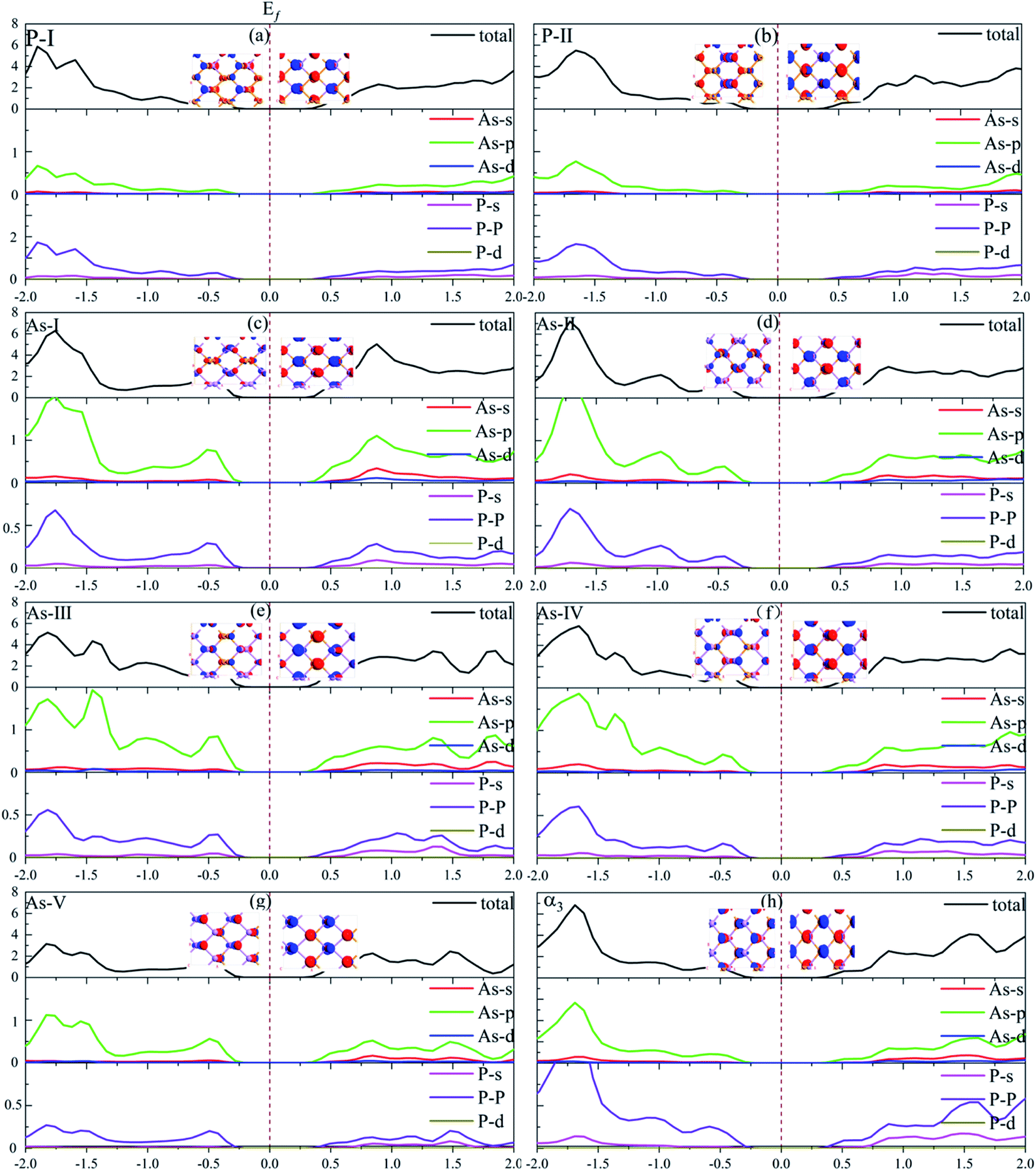
In order to analyze the differences in their electrical properties, we calculate their energy band structures. Fig. 3 shows the PBE energy band structure corresponding to these phases, among which only the energy band structure of As-IV phase has an indirect band gap. Its conduction band minimum (CBM) appears at the Γ point and valence band maximum (VBM) appears between the Γ and M points. For the energy band structure of the other phases, their VBM and CBM appear at the Γ point. Their band gaps are all around 0.90 eV, which are similar to the PBE band gap of α3 phase. Compared with the PBE band structure, the HSE06 band gap is more reflective of the true band gap of the material, and it can be seen from Table 2 that the calculated band gap of HSEO6 in the α3 phase is 1.47 eV, which is consistent with the previously reported 1.50 eV.35 The HSE06 band gaps of seven phases designed in this paper are larger than that of α3 phase, so it will have better conductivity and may have better application in power devices. In addition, we can see that the four phases As-I, As-II, As-III and As-V are similar to the α3 phase in that there is a state near the Γ point that is close to the energy of the VBM, but the two states of these four phases are almost degenerate indicating that the material can be used in p-type valley electron devices. Their density of states and the different electron orbital contributions of the atoms are shown in Fig. 4. Their electron orbitals are dominated by the outer p orbitals of the As and P atoms. The As0.25P0.75 phase has more P atoms relative to the As0.75P0.25 phase, so the orbital contribution provided by the P atoms will be larger. On the other hand, the p-orbital contribution provided by As and P atoms will be greater for P-I compared to P-II phase, and it can be seen from their MPSH diagrams that the distance between As atoms and P atoms in P-II phase will be closer, so it leads to more hybridization between them.
 |
| | Fig. 3 The PBE electronic bands corresponding to the seven phases and α3 phase. All phases are direct -gap semiconductor except As-IV phase which is an indirect-gap semiconductor. The solid red box represents the Brillouin zone path. | |
Table 2 The seven phases and α3 phase band gap under PBE and HSE06 method calculations
| Phase |
α3 |
P-I |
P-II |
As-I |
As-II |
As-III |
As-IV |
As-V |
| Band gap (eV) |
PBE |
0.90 |
0.91 |
0.91 |
0.93 |
0.90 |
0.87 |
0.88 |
0.91 |
| HSE06 |
1.47 |
1.57 |
1.54 |
1.56 |
1.52 |
1.52 |
1.52 |
1.54 |
 |
| | Fig. 4 Partial density of states and molecular projected self-consistent Hamiltonian (MPSH) corresponding to (a)–(g) the seven phases and (h) α3 phase. | |
The band structure in Fig. 3 also shows that As0.75P0.25/As0.25P0.75 phases are similar to α3 phase in that their VBM and CBM have a larger dispersion along the Γ–X direction than along the Γ–Y direction, so leading to a highly anisotropic band dispersion around the band gap. This further leads to a high anisotropy in the effective mass of the carriers in both directions. Next, we calculate the carrier mobility of these phases, Table 3 shows the effective masses and carrier mobilities of these phases along the two directions. It can be seen that the carrier mobilities of these phases along the armchair direction are generally higher than those along the zigzag direction because the armchair direction is more flexible, so the strain energy change along this direction is smaller, and the effective mass is also smaller, which are similar to the properties of As0.5P0.5 reported previously. Among these seven phases, the P-I phase has the most significant electron mobility along the armchair direction, reaching 24![[thin space (1/6-em)]](https://www.rsc.org/images/entities/char_2009.gif) 606 cm2 V−1 S−1, while the hole mobility of As-V phase along the armchair direction will be one orders of magnitude higher than the other phases, reaching 14494 cm2 V−1 S−1.
606 cm2 V−1 S−1, while the hole mobility of As-V phase along the armchair direction will be one orders of magnitude higher than the other phases, reaching 14494 cm2 V−1 S−1.
Table 3 The elastic moduli (C2D), the effective masses (m*) with respect to a free-electron mass (m0) and the carrier mobilities (u) of the seven phases along the armchair direction and zigzag. The numbers marked in bold and italic represent higher carrier mobilities
More recently, we envisioned whether strain would have a better effect on the electrical properties of these phases, so we select three phases, P-I, As-IV and As-V, to study their electronic structures under strain. Firstly, as shown in Fig. 5, we calculate the total energy of these three phases at different strains, the uniaxial strain applied only along the armchair or zigzag direction and the biaxial strain applied 1:1 to both directions simultaneously. And it can be seen that the energy of these three phases changes with strain in the same trend, with the increase of tensile strain and compressive strain the total energy of the system gradually increases; also, it can be found that the energy change of these three phases along the armchair will be smoother than along the zigzag direction. Subsequently, we calculate the band gaps of these three phases at different strains, as shown in Fig. 6, because tensile strain will strengthen the stability of the electronic structure of the material, it will lead to an increase in the band gap, and conversely, if a compressive strain is applied, it will destabilize its electronic structure and lead to the closure of the band gap, so it can be seen that the band gap gradually increases during the transition from compressive strain to tensile strain, and we found that P-I, As-V phases disappear in the simplex state at tensile strain VBM; and it is noteworthy that the As-IV phase disappears in the E(X′) degenerate state at small tensile strain, realizing the transition from indirect band gap to direct band gap. But when the tensile strain reaches a certain value, the band gap will reach an extreme value, and then there is a tendency for the band gap to become smaller. This is due to the opposite tendency of the second lower energy conduction band during the upward shift of the CBM under the action of larger tensile strains. When the strain reaches a critical value, the energies of these two energy bands reach unity. The band gap starts to decrease when the tensile strain is further increased. At the same time, it can be seen that all three phases will also undergo the transition from direct to indirect bandgap first at a certain compressive strain. From Fig. 6, it also can be seen that the transition from direct to indirect bandgap occurs at a compressive strain of −1% because of the existence of the simplex states in As-IV and As-V. For the P-I phase, the transition from direct to indirect bandgap will occur only at a very large compressive strain (−11%). This suggests that the P-I phase will be more flexible and may have better prospects for optical applications. Subsequently, the band gap is closed at a certain large compressive strain and the semiconductor-to-metallic transition occurs. But surprisingly, we find that the As-V phase undergoes three transitions under compressive strain, from semiconductor to metal at −9% compressive strain, to semiconductor again at −10%, and to metallic again at −16%; meanwhile, we explore the structures under compressive strain corresponding to the occurrence of these changes, we find that their structures are not destroyed. Also, the structural properties of the As-V phase no longer change after −16% when a higher compressive strain is applied, and are no different from the other phases.
 |
| | Fig. 5 Energy changes of the system under biaxial and uniaxial strains for (a) P-I, (b) As-IV and (c) As-V correspondingly. The red line represents the strain applied along the X (armchair) direction, the green line represents the strain applied along the Y (zigzag) direction, and the black line represents the 1:1 biaxial strain applied along both directions simultaneously. | |
 |
| | Fig. 6 Variation of band gap properties of (a) P-I, (b) As-IV and (c) As-V corresponding to biaxial and uniaxial strain. The red line represents the strain applied along the X (armchair) direction, the green line represents the strain applied along the Y (zigzag) direction, and the black line represents the 1:1 biaxial strain applied along both directions simultaneously. | |
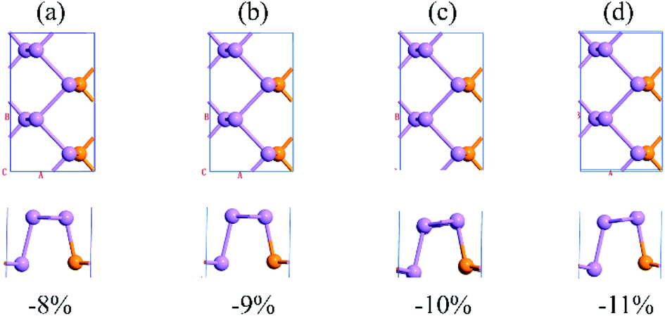
Therefore, we focus on exploring the mechanism of the semiconductor-to-metal transition of As-V at the first time (−9% to −11%). The schematic diagram of the structure under the strain range corresponding to the first transition is shown in Fig. 7, and it can be seen that the structure undergoes a relatively small deformation; analyzed from the energy perspective (shown in Fig. 8), it can be seen that the curvature of the energy change of As-V phase becomes smaller at −9% strain, and then a larger strain is applied, the curvature of the energy change returns to the same as before. The corresponding structure shows metallicity at −9% strain, and its curvature should be larger, so this is anomalous. Further we analyzed their orbital interactions, and their orbital energy band decomposition diagrams are shown in Fig. 9. It can be seen that before the metallicity transition, the VBM of As-V phase is mainly dominated by the pz orbital of As atoms, and the CBM is mainly dominated by the pz orbital of P atoms. After the metallicity transition, their orbital interactions are reversed. From their MPSH diagrams it can be seen that the orbital hybridization is stronger in the semiconductor property relative to the metal property, which is also anomalous, but it is consistent with the energy change previously studied.
 |
| | Fig. 7 The structures of As-V at (a) −8%, (b) −9%, (c) −10% and (d) −11% strain along the armchair direction. (The upper part is the top view; the lower part is the side view). | |
 |
| | Fig. 8 Energy change of the system under strain along armchair direction for As-V phase. The red box marks the variation of system energy with strain at −8% to 11% strain. | |
 |
| | Fig. 9 The PBE calculated band structure of As-V phase at (a) −8%, (b) −9%, (c) −10% and (d) −11% strain along the armchair direction, the size of the dots in the bands indicates the weight of contributions. Inset: MPSH diagrams for As-V phase under different strains along the armchair direction. | |
Fan et al. investigate the thermoelectric properties of a monolayer β-AsP3 and find that it has ultra-low thermal conductivity and ultra-high Seebeck coefficient at room temperature, with a thermoelectric figure of merit as high as 3.36 at 500 K.38 Based on this advantage, the seven α-As0.75P0.25 and As0.25P0.75 As0.75P0.25 and As0.25P0.75 phases we designed may have potential applications in thermoelectric devices. We propose their corresponding one-dimensional devices under the device schematic shown in Fig. 10; we first analyze their Seebeck effect at 300 K. The calculated Seebeck coefficients are shown in Table 4. From the table, the Seebeck coefficient of As-V is negative, which is well in line with the previous PBE energy band calculation, and the As-V phase is an n-type semiconductor. What is more exciting is that the Seebeck coefficients of the armchair type devices of P-I and P-II phases are as high as 2507 μW K−1 and 2438 μW K−1, respectively. Especially the P-II phase also has a high Seebeck coefficient of 2005 μW K−1 compared to the other phases of its zigzag type devices. In order to further characterize the thermal properties of these phases, then we calculate their thermoelectric figure of merit at 300–600 K. As shown in Fig. 11, the variation of the thermoelectric figure of merit for these seven phases with temperature is consistent with that of black arsenic phosphorus, and the overall trend is linearly increasing with temperature; for the armchair device, we can see that the As-III phase has the largest thermoelectric figure of merit, which is 10.88 at room temperature and can reach 15 at 600 K. For the zigzag device, we can see that the largest ZT value is for the As-V phase. In particular, the ZT value of the device along both directions for the As-III phase is nearly twice as high relative to the α3 phase. Taken together, the P-II and As-III phases may have better applications in thermoelectric applications compared to black phosphorus and other phases.
 |
| | Fig. 10 The schematic diagrams of the structure of (a) armchair device and (b) zigzag device composed of P-I phase (the upper part is the top view and the lower part is the side view), respectively. All one-dimensional devices are saturated by hydrogen atoms, and the ribbon width of the armchair device is 27.64 Å in the transport direction and 7.47 Å perpendicular to the transport direction, the ribbon width of the zigzag device is 19.80 Å in the transport direction and 10.20 Å perpendicular to the transport direction. | |
Table 4 Seebeck coefficients for seven phases and α3 at 300 K
| |
Phase |
P-I |
P-II |
As-I |
As-11 |
As-III |
As-IV |
As-V |
α3 |
| Seebeck coefficient (μW K−1) |
Armchair |
2507 |
2438 |
1003 |
870 |
1126 |
1188 |
−320 |
1746 |
| Zigzag |
1348 |
2005 |
1452 |
1185 |
1285 |
1608 |
489 |
1651 |
 |
| | Fig. 11 The thermoelectric advantages of the (a) armchair and (b) zigzag devices at different temperatures, respectively. | |
IV. Conclusion
In summary, using molecular dynamics simulations, we demonstrate for the first time the stability of the seven As0.25P0.75/As0.75P0.25 phases designed by first principles calculations. Their electrical, thermal properties are studied by theoretical calculations. All the considered phases are direct-gap semiconductor as the black arsenic phosphorus except for the As-IV phase, where the four phases of As-I, As-II, As-III and As-V have two degenerate VBMs. The latter indicates that these materials can be used in p-type valley electronics devices. It is also found that the P-I phase has a carrier mobility of 24606 cm2 V−1 s−1 in the armchair direction. The indirect band gap to direct band gap transition of it occurs only after application of a large compressive strain. We conclude that such a flexible two-dimensional material with large carrier mobility material may be a potential candidate for optoelectronic applications. For As-V phase, unusual change of electrical properties is obtained under applied uniaxial strain in the armchair direction. The mechanism of this phenomenon still needs to be clarified. Based on the results of the calculations of Seebeck coefficients and thermoelectric figure of merit, it is concluded that P-II and As-III phases may have wider applications in the field of thermoelectricity as compared to black and blue phosphorus. However, their stabilities require further investigations.
Conflicts of interest
There are no conflicts to declare.
Acknowledgements
The author would like to thank the National Natural Science Foundation of China under Grants (No. 11704291 and No. 51875417), Hubei Province Key Laboratory of Systems Science in Metallurgical Process (Wuhan University of Science and Technology) No. Y202101 and Key Laboratory of Nanodevices and Applications, Suzhou Institute of Nano-Tech and Nano-Bionics, Chinese Academy of Sciences No. 21YZ03, and our work is supported by High-Performance Computing Center of Wuhan University of Science and Technology.
References
- B. Aufray, A. Kara, S. Vizzini, H. Oughaddou, C. Léandri, B. Ealet and G. L. Lay, Appl. Phys. Lett., 2010, 96, 183102 CrossRef.
- B. Lalmi, H. Oughaddou, H. Enriquez, A. Kara, S. Vizzini, B. Ealet and B. Aufray, Appl. Phys. Lett., 2010, 97, 223109 CrossRef.
- Z. Shi, Z. Zhang, A. Kutana and B. I. Yakobson, ACS Nano, 2015, 9, 9802 CrossRef CAS PubMed.
- V. Y. Prinz, V. A. Seleznev, A. K. Gutakovsky, A. V. Preobrazhenskii, M. A. Putyato and T. A. Gavrilova, Phys. E, 2000, 6, 828 CrossRef CAS.
- T. Nakanishi, K. Dohmae, S. Fukui, Y. Hayashi, I. Hirose, N. Horikawa, T. Ikoma, Y. Kamiya, M. Kurashina and S. Okumi, Jpn. J. Appl. Phys., 1986, 25, 766 CrossRef CAS.
- K. S. Novoselov, A. K. Gemi, S. V. Morozov, D. Jiang, S. V. Dubonos, I. V. Grigorieva and A. A. Firsov, Science, 2004, 306, 666 CrossRef CAS PubMed.
- K. S. Novoselov, D. Jiang, F. Schedin, T. J. Booth, V. V. Khotkevich, S. V. Morozov and A. K. Geim, Proc. Natl. Acad. Sci. U. S. A., 2005, 102, 1045 CrossRef PubMed.
- A. Pakdel, Y. Bando and D. Golberg, Chem. Soc. Rev., 2014, 43, 934 RSC.
- S. J. Haigh, A. Gholinia, R. Jalil, S. Romani, L. Britnell, D. C. Elias, K. S. Novoselov, L. A. Ponomarenko, A. K. Geim and R. Gorbachev, Nat. Mater., 2012, 11, 764 CrossRef CAS PubMed.
- L. Britnell, R. Gorbachev, R. Jalil, B. Belle, F. Schedin, A. Mishchenko, T. Georgiou, M. Katsnelson, L. Eaves, S. Morozov, N. M. Peres, J. Leist, A. K. Geim, K. S. Novoselov and L. A. Ponomarenko, Science, 2012, 335, 947 CrossRef CAS PubMed.
- L. Britnell, R. M. Ribeiro, A. Eckmann, R. Jalil, B. D. Belle, A. Mishchenko, Y.-J. Kim, R. V. Gorbachev, T. Georgiou, S. V. Morozov, A. N. Grigorenko, A. K. Geim, C. Casiraghi, A. H. C. Neto and K. S. Novoselov, Science, 2013, 340, 1311 CrossRef CAS PubMed.
- C. Woods, L. Britnell, A. Eckmann, R. Ma, J. Lu, H. Guo, X. Lin, G. Yu, Y. Cao, R. Gorbachev, A. Kretinin, J. Park, L. Ponomarenko, M. Katsnelson, Y. Gornostyrev, K. Watanabe, T. Taniguchi, C. Casiraghi, H. Gao, A. Geim and K. Novoselov, Nat. Phys., 2014, 10, 451 Search PubMed.
- Z.-G. Chen, Z. Shi, W. Yang, X. Lu, Y. Lai, H. Yan, F. Wang, G. Zhang and Z. Li, Nat. Commun., 2014, 5, 4461 Search PubMed.
- A. Mishchenko, J. Tu, Y. Cao, R. Gorbachev, J. Wallbank, M. Greenaway, V. Morozov, S. Morozov, M. Zhu, S. Wong, F. Withers, C. R. Woods, Y.-J. Kim, K. Watanabe, T. Taniguchi, E. Vdovin, O. Makarovsky, T. M. Fromhold, V. I. Fal'ko, A. K. Geim, L. Eaves and K. Novoselov, Nat. Nanotechnol., 2014, 9, 808 CrossRef CAS PubMed.
- M. Khazaei, A. Mishra, N. Venkataramanan, A. Singh and S. Yunoki, Curr. Opin. Solid State Mater. Sci., 2019, 23, 164 CrossRef CAS.
- Y. Jing, X. Zhang, D. Wu, X. Zhao and Z. Zhou, J. Phys. Chem. Lett., 2015, 6, 4252 CrossRef CAS PubMed.
- H. Li, Y. Shi, M.-H. Chiu and L.-J. Li, Nano Energy, 2015, 18, 293 CrossRef CAS.
- L. Li, Y. Yu, G. J. Ye, Q. Ge, X. Ou, H. Wu, D. Feng, X. H. Chen and Y. Zhang, Nat. Nanotechnol., 2014, 9, 372 CrossRef CAS PubMed.
- M. Xie, S. Zhang, B. Cai, Z. Zhu, Y. Zou and H. Zeng, Nanoscale, 2016, 8, 13407 RSC.
- M. Xie, S. Zhang, B. Cai, Y. Zou and H. Zeng, RSC Adv., 2016, 6, 14620 RSC.
- X. Zhang, X. Zhao, D. Wu, Y. Jing and Z. Zhou, Adv. Sci., 2016, 3, 10062 Search PubMed.
- L. Bilu, M. Köpf, A. N. Abbas, W. Xiaomu, G. Qiushi, J. Yichen, X. Fengnian, R. Weihrich, F. Bachhuber, F. Pielnhofer, W. Han, R. Dhall, S. B. Cronin, G. Mingyuan, F. Xin, T. Nilgesand and Z. Chongwu, Adv. Mater., 2015, 27, 4423 CrossRef PubMed.
- M. Wu, H. Fu, L. Zhou, K. Yao and X. C. Zeng, Nano Lett., 2015, 15, 3557 CrossRef CAS PubMed.
- F. Shojaei and H. S. Kang, J. Phys. Chem. C, 2015, 119, 20210 CrossRef CAS.
- J. Qiao, X. Hu, Z.-X. Kong, F. Yang and W. Ji, Nat. Commun., 2014, 5, 4475 CrossRef CAS PubMed.
- G. Kresse and J. Hafner, Phys. Rev. B: Condens. Matter Mater. Phys., 1993, 47, 558 CrossRef CAS PubMed.
- G. Kresse and J. Furthmüller, Phys. Rev. B: Condens. Matter Mater. Phys., 1996, 54, 11169 CrossRef CAS PubMed.
- G. Kresse and D. Joubert, Phys. Rev. B: Condens. Matter Mater. Phys., 1999, 59, 1758 CrossRef CAS.
- P. E. Blöchl, Phys. Rev. B: Condens. Matter Mater. Phys., 1994, 50, 17953 CrossRef PubMed.
- J. P. Perdew and Y. Wang, Phys. Rev. B: Condens. Matter Mater. Phys., 1992, 45, 13244 CrossRef PubMed.
- A. Togo, F. Oba and I. Tanaka, Phys. Rev. B: Condens. Matter Mater. Phys., 2008, 78, 134106 CrossRef.
- J. Heyd, G. E. Scuseria and M. Ernzerhof, J. Chem. Phys., 2003, 118, 8207 CrossRef CAS.
- J. Heyd, G. E. Scuseria and M. Ernzerhof, J. Chem. Phys., 2006, 124, 219906 CrossRef.
- J. Bardeen and W. Shockley, Phys. Rev. B: Solid State, 1950, 80, 72 CrossRef CAS.
- J. Qiao, X. Kong, Z.-X. Hu, F. Yang and W. Ji, Nat. Commun., 2014, 5, 4475 CrossRef CAS PubMed.
- M. Kolos, L. Cigarini, R. Verma, F. Karlicky and S. Bhattacharya, J. Phys. Chem. C, 2021, 125, 12738–12757 CrossRef CAS.
- J. Sun, N. Lin, H. Ren, C. Tang, L. T. Yang and X. Zhao, Phys. Chem. Chem. Phys., 2016, 18, 9779 RSC.
- L. S. Fan, H. Y. Yang and G. F. Xie, Front. Mech. Eng., 2021, 7, 54 Search PubMed.
|
| This journal is © The Royal Society of Chemistry 2022 |
Click here to see how this site uses Cookies. View our privacy policy here. 
 Open Access Article
 This Open Access Article is licensed under a Creative Commons Attribution-Non Commercial 3.0 Unported Licence
 *a and
Yan Lu*b
*a and
Yan Lu*b

 is the effective mass in the transport direction and md is the average effective mass determined by
  . T is the temperature and C2D is the elastic modulus of uniform deformation of x (zigzag) and y (armchair) used to model the lattice distortion caused by strain. In the two-dimensional system, C2D can be defined as C2D = [∂2E/∂2δ2]/S0; here E is the total energy of the supercell, which is the applied uniaxial strain, and S0 is the area of the supercell in equilibrium; Ei is the DP constant which characterizes the band edge shift caused by strain and can be defined as Ei = ΔEli/(Δl/l0).