
 Open Access Article
 This Open Access Article is licensed under a Creative Commons Attribution-Non Commercial 3.0 Unported Licence
A first-principles study of electronic and optical properties of the tetragonal phase of monolayer ZnS modulated by biaxial strain
Bin Liua,
Wan-Sheng Su *bcd and
Bi-Ru Wue
*bcd and
Bi-Ru Wue
aSchool of Mathematics and Physics, Nanyang Institute of Technology, Nanyang 473004, China
bNational Taiwan Science Education Center, Taipei 11165, Taiwan. E-mail: wssu@mail.ntsec.gov.tw
cDepartment of Electro-Optical Engineering, National Taipei University of Technology, Taipei 10608, Taiwan
dNational Applied Research Laboratories, Taiwan Semiconductor Research Institute, Hsinchu 30078, Taiwan
eDivision of Natural Science, Center for General Education, Chang Gung University, Tao-Yuan 33302, Taiwan
First published on 21st February 2022
Abstract
Modulation of the electronic and optical properties of two-dimensional (2D) materials is of great significance for their practical applications. Here, by using first-principles calculations, we study a tetragonal phase of monolayer ZnS, and explore its associated electronic and optical properties under biaxial strain. The results from phonon dispersion and molecular dynamics simulation demonstrate that the tetragonal phase of monolayer ZnS possesses a very high stability. The monolayer ZnS has a direct band gap of 4.20 eV. It changes to an indirect band gap under both compression and tension, exhibiting a decrease in band gap. However, the band gap decreases more slowly under compression compared to the tension process such that the direct band gap remains within −8%, demonstrating excellent endurance under pressure. Fortunately, tetragonal ZnS exhibits a good absorption ability in the ultraviolet (UV) range regardless of strain. Our research results enrich the understanding of monolayer ZnS, which is helpful for the design and application of optoelectronic devices using the material.
1. Introduction
Binary II–VI zinc chalcogenides have attracted significant interest due to their potential suitability for a broad range of optoelectronic and thermoelectric applications.1–4 Three-dimensional (3D) ZnS exhibits the wurtzite (WZ) phase at high temperatures, and the cubic zinc blende (ZB) structure at low temperatures and ambient pressure with a wide band gap of 3.77 eV,5 making it an outstanding candidate for nanoelectronic devices such as short-wavelength light-emitting devices. In addition, the zero-dimensional (0D) quantum dots of ZnS have been synthesized to further improve photoelectric efficiency.6,7 Since the discovery of graphene,8 much effort has been expended in exploring two-dimensional (2D) layered materials because of their novel electrical and optical performances which vary distinctly from the bulk phases.9–11The freestanding monolayer ZnS is a honeycomb structure just like graphene, which has been previously experimentally obtained.12–14 Investigations of electronic and optical properties of graphene-like 2D ZnS reveal that the 2D ZnS has an ultrawide band gap of 4.3 eV,15 and the transparency of 2D ZnS is greater than that of the 3D phase over the visible range.16 To deepen the understanding of the graphene-like 2D ZnS, Peng et al. studied its mechanical behavior.17 Krainara et al. rolled it to the single-walled nanotube to improve its electronic performance.18 In addition, strain modulation and element doping in the 2D ZnS have also been carried out.15,19,20 Recently, a tetragonal phase has been reported in monolayer CdTe,21 CdSe,22 CdS22 and ZnSe;23 as one of these II–VI compounds, monolayer ZnS also possesses a similar structure.24 However, the knowledge of monolayer tetragonal ZnS remains very limited,25 which severely impedes its practical application.
In this work, we have studied the electronic and optical properties of the tetragonal phase of monolayer ZnS, and then explored the influences of applied biaxial strain by using ab initio calculations. There is no imaginary frequency in the phonon spectrum for monolayer tetragonal ZnS, suggesting its dynamical stability. Endurance at 800 K in molecular dynamics (MD) simulation indicates that the monolayer tetragonal ZnS also possesses a high thermodynamics stability. Similar to the honeycomb phase of monolayer ZnS,15 the tetragonal ZnS also exhibits an ultrawide direct band gap, and shows excellent optical absorption in the UV range. In addition, although the band gap of monolayer ZnS changes with strain, this good absorption ability in UV remains. Our findings deepen the understanding of monolayer ZnS, which could speed up its application in optoelectronic devices.
2. Computational details
We performed the first-principles calculations using the Vienna ab initio simulation package (VASP) based on the density functional theory (DFT).26,27 The projector augmented-wave (PAW) method28 and Perdew–Burke–Ernzerhof generalized gradient approximation (GGA-PBE) were utilized to describe the exchange-correlation functional.29 The kinetic energy cutoff was set to 500 eV, and k-point meshes of 10 × 10 × 1 were chosen from the Brillouin zone with the Monkhorst–Pack method.30 For structural relaxation, the convergence values were 10−6 eV per atom and 0.01 eV Å−1 for total energy and atomic force component, respectively. A biaxial strain was applied to modulate the electronic and optical properties of monolayer tetragonal ZnS with a strain range from −10% to 10%, corresponding to the compression and tension stages. For calculations of electronic and optical properties, monolayer ZnS was simulated in a periodic 1 × 1 slab with a vacuum thickness of 20 Å. The hybrid Heyd–Scuseria–Ernzerhof (HSE06) functional was applied to obtain more accurate electronic structures and optical properties.31 In addition, the DFT-D3 method from Grimme was utilized to correct the long-range vdW interaction.32 The phonon band structure was calculated by the Phonopy package.33 For the MD simulations, a 4 × 4 supercell was utilized to explore the dynamics stability of monolayer ZnS. Only one Γ point was sampled in the Brillouin zone, with a time step of 1 fs. The canonical (NVT) ensemble with Nosé–Hoover thermostat was applied to maintain the temperature during the relaxation stage.3. Results and discussion
Fig. 1(a) shows the top and side views of the monolayer tetragonal ZnS, in which Zn is in a tetrahedral environment while S is in a pyramid structure. The calculated lattice constant is 3.96 Å, which is close to the value in previous literature.25 To validate the calculations, the bond length of the graphene-like 2D ZnS is also calculated as having a value of 2.24 Å, in line with a previous report.15 In addition, the exfoliation energy of monolayer tetragonal ZnS from the five-layer stack structure is identified as low as 0.39 J m−2, indicating that the interlayer interaction of monolayer tetragonal ZnS is sufficiently small such that the monolayer tetragonal ZnS possesses high stability.34 Fig. 1(b) shows the phonon dispersion curves of monolayer ZnS with a supercell of 4 × 4 × 1. There is no imaginary frequency in the phonon band, demonstrating the dynamical stability of monolayer tetragonal ZnS. The ab initio molecular dynamics (AIMD) results of a ZnS supercell under different strains are shown in Fig. 1(c). For the ZnS supercell without strain, the total energy fluctuates notably in the initial stage, but quickly becomes stable with longer simulation time. There is no abrupt variation in total energy during the subsequent MD simulations, indicating that the chemical bonds in tetragonal ZnS are very stable. The inset snapshot presents the final configuration of this ZnS supercell. Although many atoms clearly deviate from their equilibrium positions, the local chemical environment remains for both Zn and S, giving the ZnS supercell a high thermodynamic stability. When the strain is applied, the ZnS supercell stabilizes at 400 K under a strain of −4% and at 700 K at a strain of 4%, indicating that the thermal stability is reduced under both compression and tension processes. Fig. 1(d) shows the strain energies of monolayer ZnS at different strains. The strain energy is at its minimum for the monolayer ZnS at zero strain. The strain energy increases quickly under compression while it increases more slowly in the tension process, suggesting that the tetragonal ZnS resists pressure more.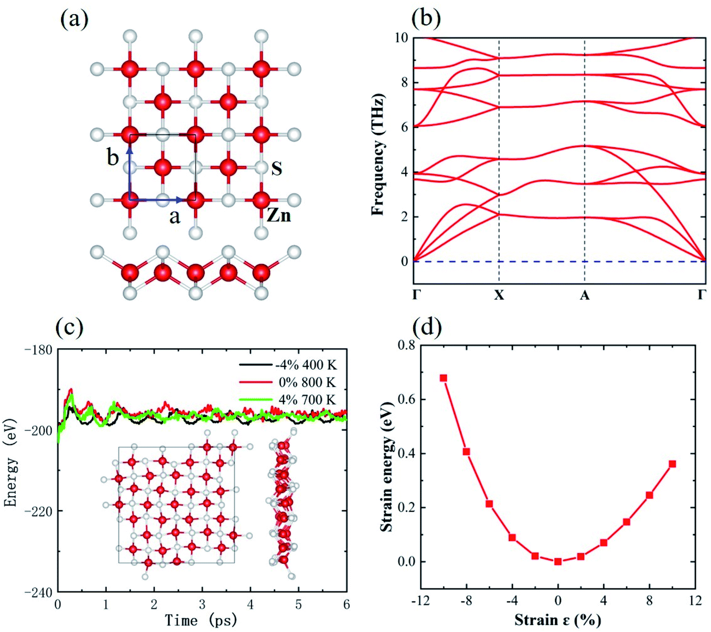 | ||
| Fig. 1 (a) Top and side views, (b) phonon band dispersion, (c) evolution of total energies with time in the AIMD process under different strains, and (d) strain energy–strain curve of monolayer ZnS. | ||
Fig. 2(a) shows the electronic band structures of the monolayer tetragonal ZnS using the PBE method, and the PBE method with HSE06 correction, with the inset schematic showing the K path in the Brillouin zone. Both the valence band maximum (VBM) and the conduction band minimum (CBM) are located at the Γ point, demonstrating that monolayer tetragonal ZnS possesses a direct band gap. The band gaps are 2.91 eV and 4.20 eV for PBE and PBE with the HSE06 hybrid functional, respectively, indicating that the monolayer tetragonal ZnS is an ultrawide-bandgap semiconductor.35 The electronic structures of the two methods are close in the valence bands, but clearly different in the conduction bands. This difference is due to the underestimation of the PBE method in the exchange–correlation functional. The partial density of state (PDOS) of the monolayer tetragonal ZnS is shown in Fig. 2(b). The valence band near VBM is dominantly contributed by the p state of S and the p and d states of Zn, of which the p state of S is predominant, while the s state of Zn is mainly responsible for the CBM of the monolayer ZnS.
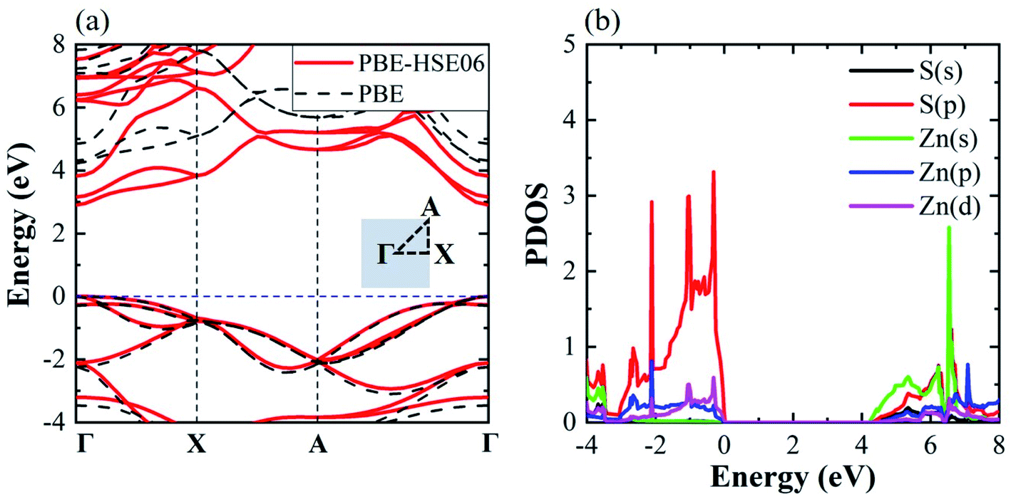 | ||
| Fig. 2 (a) The electronic band structures and (b) The PDOS of the monolayer ZnS. | ||
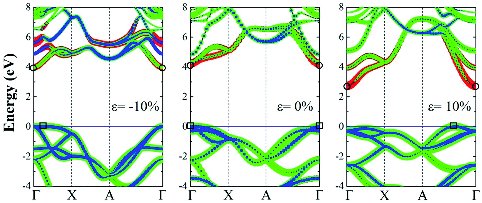
When a biaxial strain is applied to the tetragonal monolayer ZnS, the electronic and optical properties will change with the lattice length. Fig. 3 shows the electronic band structure obtained from the PBE method with HSE06 hybrid functional under different strains, corresponding to the compression (0– −10%) and tension (0–10%) processes. In compression process, both the VBM and CBM are located at the Γ point under strains of −4% and −8%, exhibiting the direct band gaps of 4.23 eV and 4.08 eV, respectively. However, the VBM right shifts to the Γ–X region when the strain reaches −10%, resulting in an indirect band gap of 3.98 eV. As for the tension process, the CBM are always located at the Γ point while the VBM is located between the Γ and A points, exhibiting indirect band gaps of 3.69 eV, 3.02 eV and 2.72 eV at strains of 4%, 8% and 10%, respectively. It is clear that the band structure of monolayer ZnS changes from a direct band gap to an indirect band gaps under both compression and tension processes due to the migration of VBM. However, note that the positions of VBM are along the Γ–X path for compressive strain but along A–Γ for tensile strains.
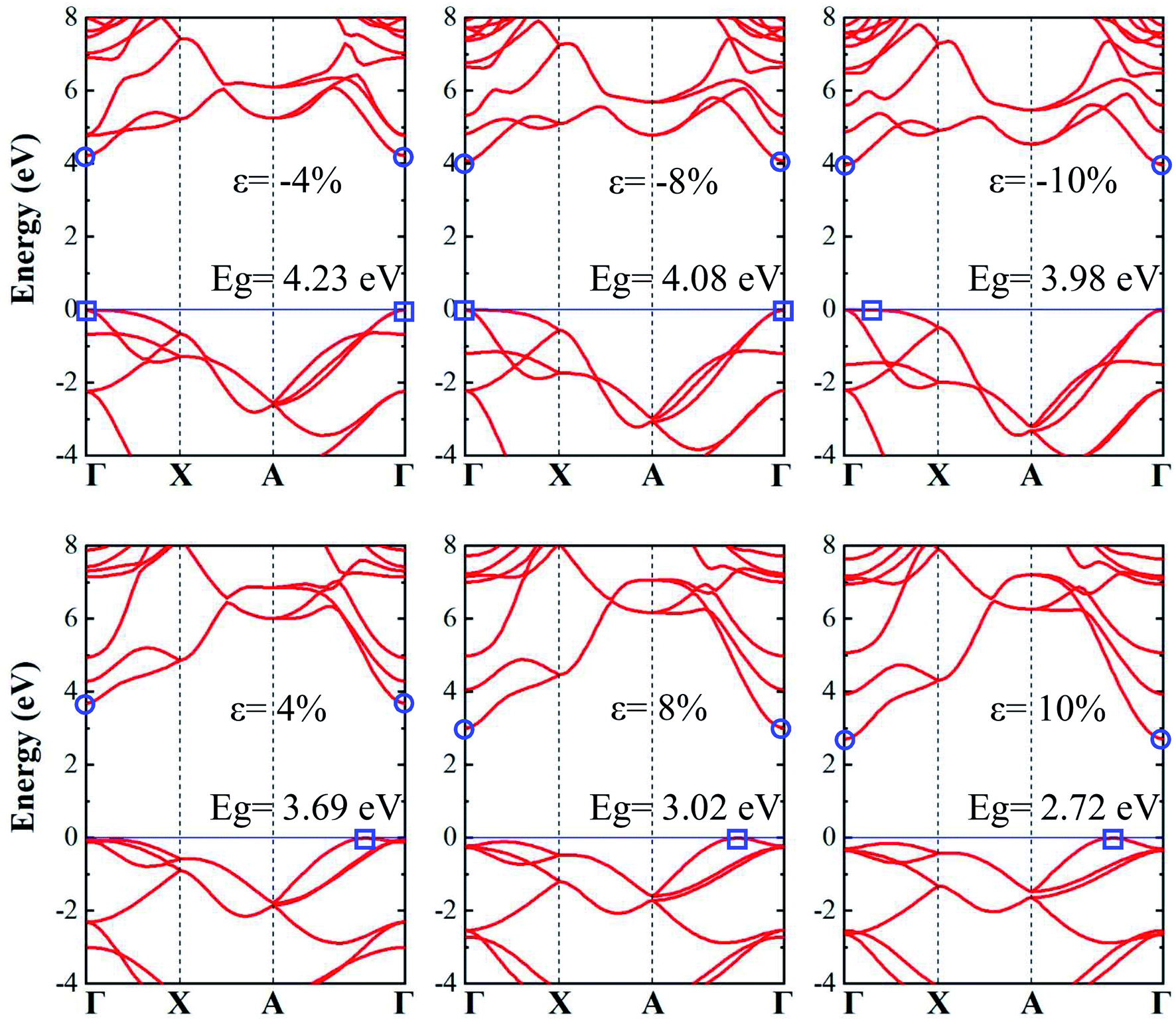 | ||
| Fig. 3 The electronic band structures of monolayer ZnS under compression and tension. The circle and rectangle symbols represent the CBM and VBM, respectively. | ||
Fig. 4(a) shows the evolution of band gap with the strain, calculated by the PBE method, and the PBE method with HSE06 correction, respectively. The two band gap curves show a similar tendency in both compression and tension processes regardless of the differences in band gap. The band gap increases at first and then decreases slightly during the compression process, whereas the band gap gradually decreases in the tension process. Note that the band gap varies by a relatively smaller amount in the compression process as compared to the tension process. The band structures during the strain scale ranging from −8% to 2% exhibit direct band gaps, denoted by the grey region of Fig. 4(a), but become indirect when the strain exceeds that range. Fig. 4(b–d) shows the charge distributions of monolayer tetragonal ZnS under strains of 0%, −10% and 10%, respectively. For the monolayer ZnS with a strain of −10%, the interatomic distance becomes smaller, increasing the charge between Zn and S, as seen in Fig. 4(c). In contrast, the charge between Zn and S decreases when the strain is 10%, owing to the weak effect between Zn and S, as shown in Fig. 4(d).
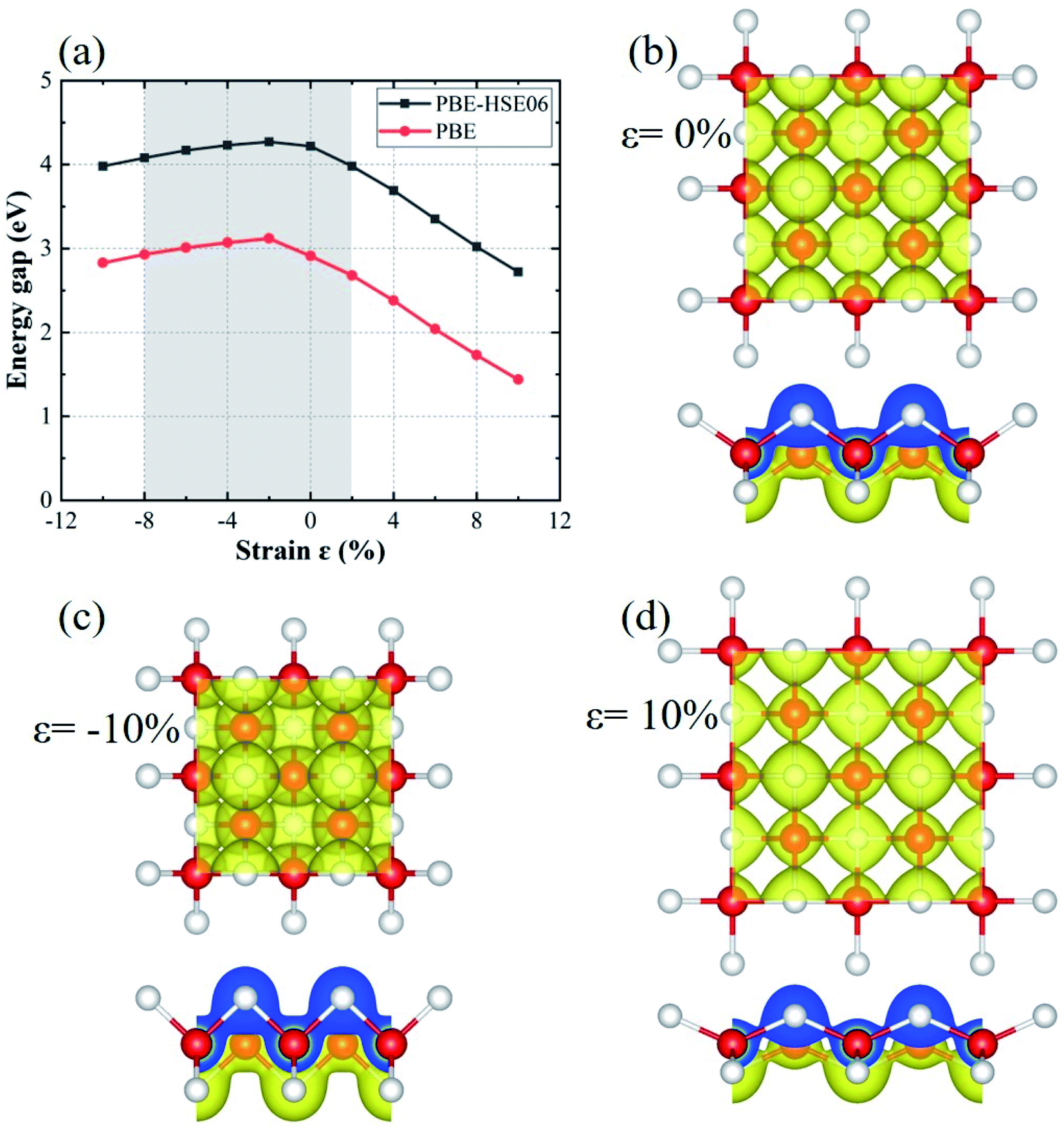 | ||
| Fig. 4 (a) The energy bandgap of monolayer ZnS with strain, and (b–d) the charge distributions of monolayer ZnS under strains of 0%, −10% and 10%, respectively. The yellow areas show the charge density with an iso-value of 0.02 Å−2, while the blue regions are the sectional view of charge distributions. | ||
Fig. 5 shows the projected band structures of monolayer ZnS under different strains. For the monolayer ZnS without strain (0%), the VBM is dominantly contributed by the p orbit while the CBM's major contributor is the s orbit. For a compression strain of −10%, the VBM right shifts to the Γ–X region due to the upshift of the p orbit, while the CBM shifts down slightly at the Γ point, which is mainly ascribed to the movement of the s orbit. At a tension strain of 10%, the VBM is mostly contributions of the p orbit, and moves to the A–Γ region, while the CBM decreases due to the downshift of the s orbit. It can be seen that the CBM is always located at the Γ point, while the VBM varies with strain, resulting in the direct–indirect transition. As the p orbit plays an important role in the variation of the VBM, it is believed to be the origination of the transition.
 | ||
| Fig. 5 The projected band structures under strains of −10%, 0% and 10%. The red, green and blue symbols represent the contributions from the s, p and d orbits, where the width represents the weight. The black squares and circles show the VBM and CBM, respectively. | ||
Fig. 6 shows the PDOS of monolayer tetragonal ZnS under different strains, which are calculated with the tetrahedron method for Blöchl corrections, and a smearing width of 0.05 eV. Fig. 6(a) and (b) show the PDOS of Zn and S under different strains, respectively. From Fig. 5, the VBM of such a monolayer ZnS is mainly composed of the p state, while the CBM is ascribed to the s state. In the compression process, the d state of Zn near the VBM varies little, while the p state of S changes notably, in which the py and pz states are notably reduced. The s state of Zn on the conduction band gradually decreases as well as the p state of S. In the tension process, the dx2 states of Zn in the vicinity of the VBM increases, while the py state of S increases prominently. The s state of Zn at the CBM decreases notably while the electronic states of S change little. Comparing the PDOS of Zn and S with strain, note that the electronic states at the VBM are mainly composed of the p states of S, while the CBM is dominantly made up of contributions from the s states of Zn. As the p state of S shows two different evolution tendencies under compression and tension, thus the transitions of the band structure from direct gap to indirect gap exhibit two different behaviors.
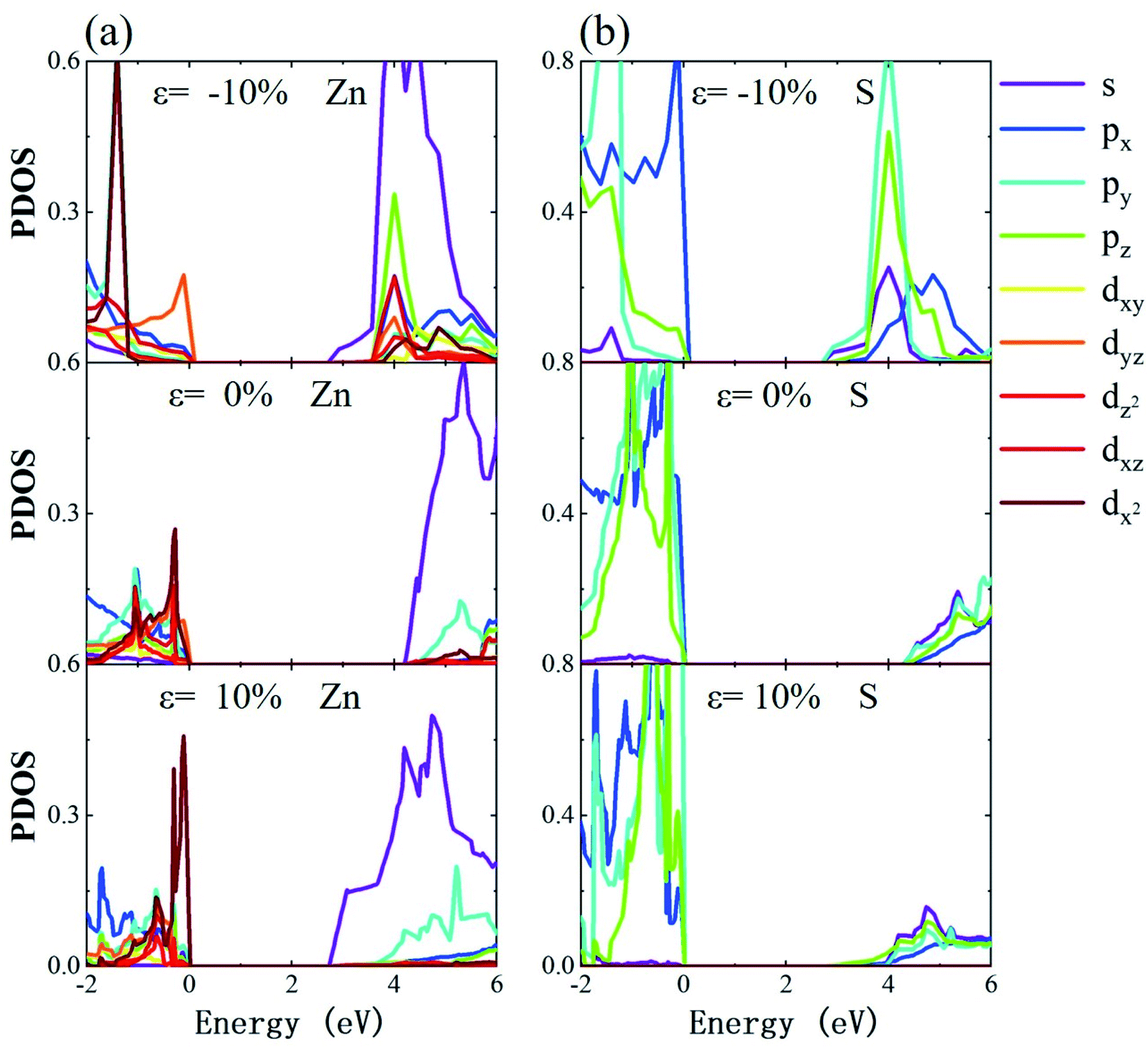 | ||
| Fig. 6 The PDOS of (a) Zn and (b) S under different strains. | ||
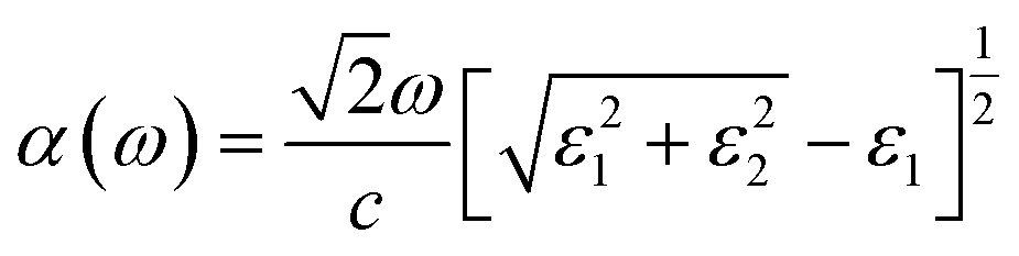
The optical absorptions α(ω) of monolayer tetragonal ZnS under different strains are obtained from the real (ε1) and imaginary (ε2) parts of the dielectric function. The formula is as follows:
 | (1) |
Fig. 7 shows the optical absorption spectrum, in which the HSE06 correction is applied for more accurate results. The results present strong light absorption peaks in the UV spectrum, as most of the absorption spectrum lies above 3.1 eV. There are two prominent absorption ranges for monolayer ZnS without strain, located at 3.1–5.8 eV and 5.8–10 eV. In the compression process, the strength of the first absorption range was gradually reduced, while the second absorption range evolves to a notable peak, suggesting that absorption ability in this range increases with compression. In the tension process, the first absorption range increases to a notable peak, while the second absorption range decreases, with the absorption ability enhanced in the first absorption range. This indicates that monolayer ZnS exhibits an excellent absorption ability in the UV region, with strain effectively tuning the absorption range to the UV spectrum. Although the absorption peak changes with the strain, the absorption spectrum is always concentrated in the UV region regardless of the applied strain. This is probably due to the stable direct band gap and its large value under strain. In addition, optical absorption below 3.1 eV changes little with strain, suggesting that the tetragonal phase of monolayer ZnS possesses excellent transmission in the visible and infrared regions. Therefore, it still could act as the shell for quantum dots and optical films.36
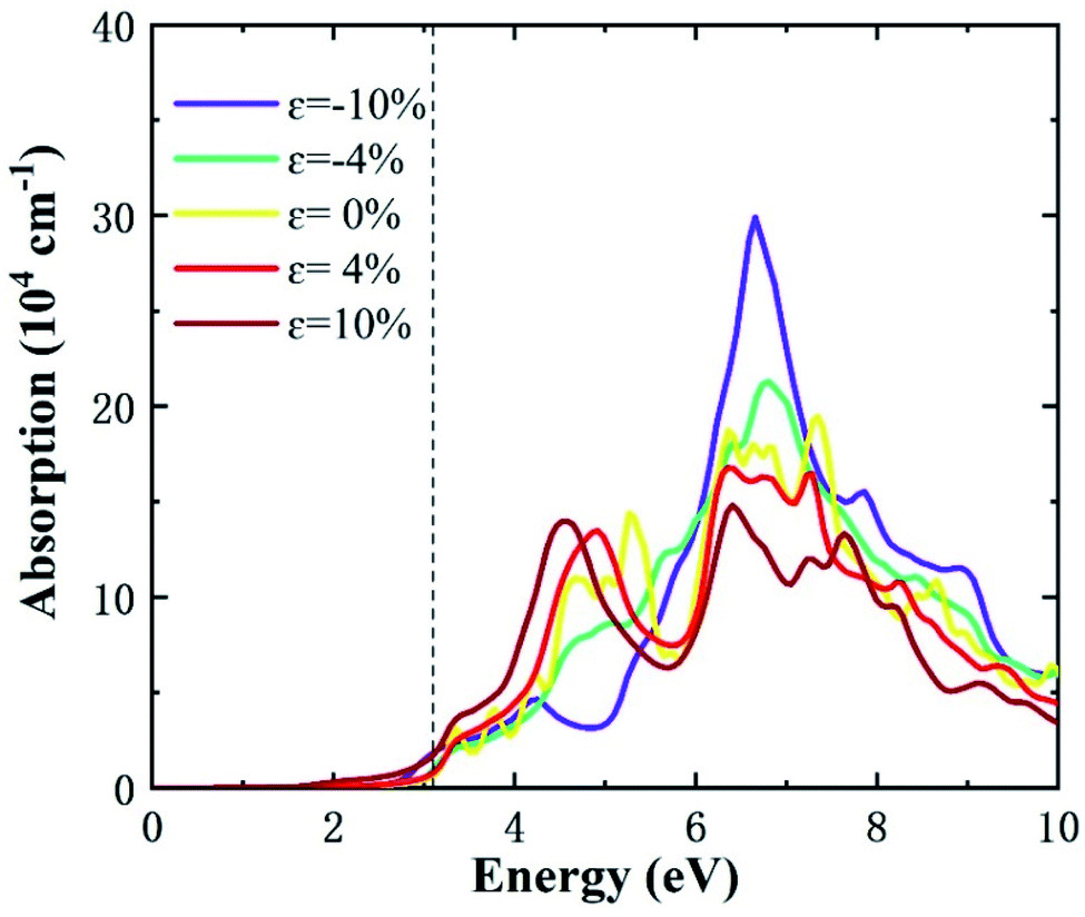 | ||
| Fig. 7 Optical absorption of the monolayer ZnS under different strains. Dashed line represents the absorption edge of UV light. | ||
4. Conclusions
In summary, we investigated the electronic and optical characteristics of the tetragonal phase of monolayer ZnS using the first principles calculation, and explored their evolutions with strain. There is no imaginary frequency in phonon band and the monolayer ZnS can endure the thermal fluctuation at 800 K for a long time, certifying the stability of the monolayer ZnS with a tetragonal structure. The monolayer ZnS is a direct band gap semiconductor with an ultrawide band gap of 4.20 eV, and maintains the direct gap over the strain range from −8% to 2%. Beyond this scope, the band structure becomes indirect due to the migration of the VBM. Though the band gap decreases in both compression and tension processes, the extent of decrease under tension is substantially larger. Fortunately, the optical absorption of monolayer ZnS always exhibits good performance in the UV range regardless of variation in strain, suggesting that monolayer ZnS is a good candidate for a UV detector. Further, the excellent transmission in both visible and infrared regions ensures that it is a good candidate for the shells of photoelectric devices.Conflicts of interest
There are no conflicts to declare.Note added after first publication
This article replaces the version published on 21st February 2022, which contained an error relating to the compression percentage.Acknowledgements
W.-S. Su would like to thank the Ministry of Science and Technology for financially supporting this research under Contract No. MOST-110-2112-M-979-001. Support from the National Centers for Theoretical Sciences and High-performance Computing of Taiwan in providing significant computing resources to facilitate this research are also gratefully acknowledged.References
- Y. Sun, Z. Sun, S. Gao, H. Cheng, Q. Liu, J. Piao, T. Yao, C. Wu, S. Hu, S. Wei and Y. Xie, Nat. Commun., 2012, 3, 1057 CrossRef PubMed.
- Y. Zhang, N. Zhang, Z.-R. Tang and Y.-J. Xu, ACS Nano, 2012, 6, 9777–9789 CrossRef CAS PubMed.
- X. Fang, T. Zhai, U. K. Gautam, L. Li, L. Wu, Y. Bando and D. Golberg, Prog. Mater. Sci., 2011, 56, 175–287 CrossRef CAS.
- Y. Hinuma, A. Grüneis, G. Kresse and F. Oba, Phys. Rev. B: Condens. Matter Mater. Phys., 2014, 90, 155405 CrossRef.
- J. X. Ding, J. A. Zapien, W. W. Chen, Y. Lifshitz, S. T. Lee and X. M. Meng, Appl. Phys. Lett., 2004, 85, 2361–2363 CrossRef CAS.
- Y.-W. Jun, J.-S. Choi and J. Cheon, Angew. Chem., Int. Ed. Engl., 2006, 45, 3414–3439 CrossRef CAS PubMed.
- Y. W. Zhao, Y. Zhang, H. Zhu, G. C. Hadjipianayis and J. Q. Xiao, J. Am. Chem. Soc., 2004, 126, 6874–6875 CrossRef CAS PubMed.
- K. S. Novoselov, A. K. Geim, S. V. Morozov, D. Jiang, Y. Zhang, S. V. Dubonos, I. V. Grigorieva and A. A. Firsov, Science, 2004, 306, 666–669 CrossRef CAS PubMed.
- H. Shen, R. Yang, K. Xie, Z. Yu, Y. Zheng, R. Zhang, L. Chen, B.-R. Wu, W.-S. Su and S. Wang, Phys. Chem. Chem. Phys., 2022, 24, 357–365 RSC.
- J. Wang, Y. Guo, C. Qiao, H. Shen, R. Zhang, Y. Zheng, L. Chen, S. Wang, Y. Jia and W.-S. Su, Chin. J. Phys., 2019, 62, 172–178 CrossRef CAS.
- Z. Wang, F. Dong, B. Shen, R. J. Zhang, Y. X. Zheng, L. Y. Chen, S. Y. Wang, C. Z. Wang, K. M. Ho, Y.-J. Fan, B.-Y. Jin and W.-S. Su, Carbon, 2016, 101, 77–85 CrossRef CAS.
- X. Huang, J. Li and H. Fu, J. Am. Chem. Soc., 2000, 122, 8789–8790 CrossRef CAS.
- X. Huang, J. Li, Y. Zhang and A. Mascarenhas, J. Am. Chem. Soc., 2003, 125, 7049–7055 CrossRef CAS PubMed.
- X. Huang and J. Li, J. Am. Chem. Soc., 2007, 129, 3157–3162 CrossRef CAS PubMed.
- A. Es-Smairi, N. Fazouan, E. H. Atmani, M. Khuili and E. Maskar, Appl. Phys. A, 2021, 127, 698 CrossRef CAS.
- H. Lashgari, A. Boochani, A. Shekaari, S. Solaymani, E. Sartipi and R. T. Mendi, Appl. Surf. Sci., 2016, 369, 76–81 CrossRef CAS.
- Q. Peng, L. Han, X. Wen, S. Liu, Z. Chen, J. Lian and S. De, RSC Adv., 2015, 5, 11240–11247 RSC.
- N. Krainara, J. Limtrakul, F. Illas and S. T. Bromley, Phys. Rev. B: Condens. Matter Mater. Phys., 2011, 83, 233305 CrossRef.
- R. Chaurasiya, A. Dixit and R. Pandey, J. Appl. Phys., 2019, 125, 082540 CrossRef.
- M. Jafari and K. Alvani, Mater. Res. Express, 2019, 6, 0850b5 CrossRef CAS.
- E. Unsal, R. T. Senger and H. Sahin, J. Mater. Chem. C, 2017, 5, 12249–12255 RSC.
- M. Naseri, A. Bafekry, M. Faraji, D. M. Hoat, M. M. Fadlallah, M. Ghergherehchi, N. Sabbaghi and D. Gogova, Phys. Chem. Chem. Phys., 2021, 23, 12226–12232 RSC.
- L. Li, P. Li, N. Lu, J. Dai and X. C. Zeng, Adv. Sci., 2015, 2, 1500290 CrossRef PubMed.
- C.-J. Tong, H. Zhang, Y.-N. Zhang, H. Liu and L.-M. Liu, J. Mater. Chem. A, 2014, 2, 17971–17978 RSC.
- J. Zhou and X. Wu, J. Alloys Compd., 2017, 695, 1392–1396 CrossRef CAS.
- G. Kresse and J. Hafner, Phys. Rev. B: Condens. Matter Mater. Phys., 1993, 47, 558–561 CrossRef CAS PubMed.
- G. Kresse and J. Furthmüller, Phys. Rev. B: Condens. Matter Mater. Phys., 1996, 54, 11169–11186 CrossRef CAS PubMed.
- P. E. Blöchl, Phys. Rev. B: Condens. Matter Mater. Phys., 1994, 50, 17953–17979 CrossRef PubMed.
- J. P. Perdew, K. Burke and M. Ernzerhof, Phys. Rev. Lett., 1996, 77, 3865–3868 (Phys. Rev. Lett., 1997, 78, 1396) CrossRef CAS PubMed ).
- H. J. Monkhorst and J. D. Pack, Phys. Rev. B: Solid State, 1976, 13, 5188–5192 CrossRef.
- J. Heyd, G. E. Scuseria and M. Ernzerhof, J. Chem. Phys., 2003, 118, 8207–8215 CrossRef CAS.
- S. Grimme, J. Antony, S. Ehrlich and H. Krieg, J. Chem. Phys., 2010, 132, 154104 CrossRef PubMed.
- A. Togo, F. Oba and I. Tanaka, Phys. Rev. B: Condens. Matter Mater. Phys., 2008, 78, 134106 CrossRef.
- J. H. Jung, C.-H. Park and J. Ihm, Nano Lett., 2018, 18, 2759–2765 CrossRef CAS PubMed.
- J. Y. Tsao, S. Chowdhury, M. A. Hollis, D. Jena, N. M. Johnson, K. A. Jones, R. J. Kaplar, S. Rajan, C. G. Van de Walle, E. Bellotti, C. L. Chua, R. Collazo, M. E. Coltrin, J. A. Cooper, K. R. Evans, S. Graham, T. A. Grotjohn, E. R. Heller, M. Higashiwaki, M. S. Islam, P. W. Juodawlkis, M. A. Khan, A. D. Koehler, J. H. Leach, U. K. Mishra, R. J. Nemanich, R. C. N. Pilawa-Podgurski, J. B. Shealy, Z. Sitar, M. J. Tadjer, A. F. Witulski, M. Wraback and J. A. Simmons, Adv. Electron. Mater., 2018, 4, 1600501 CrossRef.
- Z. Quan, Z. Wang, P. Yang, J. Lin and J. Fang, Inorg. Chem., 2007, 46, 1354–1360 CrossRef CAS PubMed.
| This journal is © The Royal Society of Chemistry 2022 |