
 Open Access Article
 This Open Access Article is licensed under a Creative Commons Attribution-Non Commercial 3.0 Unported Licence
Effect of lattice mismatch on film morphology of the quasi-one dimensional conductor K0.3MoO3
Yifeng Cao a,
Nicholas Russoa,
Lei Gaob,
Ailing Jib,
Linda H. Doerrera,
Nianpeng Lub and
Kevin E. Smith*a
a,
Nicholas Russoa,
Lei Gaob,
Ailing Jib,
Linda H. Doerrera,
Nianpeng Lub and
Kevin E. Smith*a
aDepartment of Physics, Boston University, Boston, Massachusetts 02215, USA. E-mail: ksmith@bu.edu; Tel: +1-617-353-6117
bInstitute of Physics, Chinese Academy of Sciences, Beijing, 100190, China
First published on 3rd February 2022
Abstract
High quality epitaxial thin films of the quasi-one dimensional conductor K0.3MoO3 have been successfully grown on SrTiO3(100), SrTiO3(110), and SrTiO3(510) substrates via pulsed laser deposition. Scanning electron microscopy revealed quasi-one dimensional rod-shaped structures parallel to the substrate surface, and the crystal structure was verified by using X-ray diffraction. The temperature dependence of the resistivity for the K0.3MoO3 thin films demonstrates a metal-to-semiconductor transition at about 180 K. Highly anisotropic resistivity was also observed for films grown on SrTiO3(510).
1 Introduction
Quasi-low-dimensional solids are important materials for both fundamental research and applied science.1,2 For example, quasi-one-dimensional organic salts TTF-TCNQ, (TMTTF)2X, etc. are bulk three-dimensional compounds.3 The carrier motion therein is restricted to two-dimensional atomic layers, or one-dimensional chains, yet the Coulomb force remains three-dimensional in character, due to the anisotropy of transfer integrals between different chemical units. This enables these quasi-low-dimensional solids to be ideal platforms for the observation of Wigner crystallization.Among quasi-low-dimensional solids, blue molybdenum bronze (A0.3MoO3, A = K, Rb, Tl) attracted our attention with the availability of large-sized, high-quality crystals.4 Blue molybdenum bronzes (BMBs) are known for charge density wave (CDW) behaviors in which Peierls predicted that the electron density would show periodic fluctuations by the rearrangement of the ion cores causes a metal to semiconductor Peierls transition with transition temperature about 182 K.5 BMBs have monoclinic symmetry with 20 molecular formula per unit cell in space group C2/m.6 The structure of the BMBs is composed of infinite chains of MoO6 octahedra with A cations located at sharing corners along the monoclinic b direction. The conductive chain structure not only makes the BMBs good candidates as CDW materials where the motion of electrons is restricted to the c axis but also, unlike NbSe3 (ref. 7) and TaS3,8 remain unchanged when we modify the interchain interactions. It is of importance to prepare thin films of quasi-low dimensional BMBs in order to probe the role of film thickness on CDW behavior. In this paper, we focus on preparing crystalline thin films for blue bronze K0.3MoO3 (a = 18.249 Å, b = 7.560 Å, c = 9.855 Å, β = 117°32′ (ref. 6)).
Bulk K0.3MoO3 was first synthesized by Wold et al. in 1964 by electrolytic reduction of K2MoO4–MoO3 melts under desired temperature.9 Synthesis of nanoscaled crystalline K0.3MoO3, however, remained a hard task. CDW material like NbSe3 (ref. 10) and TaS3 (ref. 11) were prepared by chemical vapor transport method. Takamasa et al. applied this method on BMBs but did not work. Then they tried hydrothermal method on K0.3MoO3 and successfully prepared the nanoribbons of K0.3MoO3.12 The crystalline Rb0.3MoO3 thin film was prepared by van der Zant et al. using pulsed laser deposition.13 Dominko et al. applied the same method on K0.3MoO3 and got the thin films of about 100 nm in thickness on Al2O3(1![[1 with combining macron]](https://www.rsc.org/images/entities/char_0031_0304.gif) 02) substrate and SrTiO3(510) substrate.14 However, the resistivity of their thin film is even an order higher than the least conducting direction of bulk K0.3MoO3 and no metal to semiconductor transition is observed.
02) substrate and SrTiO3(510) substrate.14 However, the resistivity of their thin film is even an order higher than the least conducting direction of bulk K0.3MoO3 and no metal to semiconductor transition is observed.
In this study, we applied pulsed laser deposition to synthesize K0.3MoO3 on SrTiO3(100), SrTiO3(110) and SrTiO3(510) substrates, respectively. High-quality crystalline samples about 100 nm in thickness were obtained, and typical temperature dependence of electrical resistivity indicates the occurrence of metal to semiconductor transition at about 180 K. The anisotropic electrical resistivity confirms the quasi-one dimensional nature of the films.
2 Experimental
2.1 Sample preparation
The K0.3MoO3 target for PLD growth was fabricated in a vacuum furnace, with a mixture of K2O and MoO3 in the molar ratio of 0.15![[thin space (1/6-em)]](https://www.rsc.org/images/entities/char_2009.gif) :1, calcined at 1500 °C and then pressed into a pellet. The PLD laser source was a KrF Compex Pro 205F manufactured by Coherent, operating at a wavelength of 248 nm. The substrates were 5 × 5 × 0.5 mm and preprocessed with a plasma cleaner. The distance between the substrate and the target was set at 65 mm. We found the best quality K0.3MoO3 thin films were grown with a 52 mJ pulse energy, corresponding to an energy density of 13 mJ mm−2, and an oxygen pressure of 8 Pa. The temperature of the substrate was set to 450 °C for SrTiO3(100) substrates and 400 °C for the SrTiO3(110) and SrTiO3(510) substrates. The frequency of the laser seeming did not affect the quality of the thin film because the duration of the laser pulse is only 25 ns which means the plume has enough relaxation time from pulse to pulse. In this study, we set the laser frequency to 4 Hz in order to achieve a moderate growing speed of about 5 nm min−1.
:1, calcined at 1500 °C and then pressed into a pellet. The PLD laser source was a KrF Compex Pro 205F manufactured by Coherent, operating at a wavelength of 248 nm. The substrates were 5 × 5 × 0.5 mm and preprocessed with a plasma cleaner. The distance between the substrate and the target was set at 65 mm. We found the best quality K0.3MoO3 thin films were grown with a 52 mJ pulse energy, corresponding to an energy density of 13 mJ mm−2, and an oxygen pressure of 8 Pa. The temperature of the substrate was set to 450 °C for SrTiO3(100) substrates and 400 °C for the SrTiO3(110) and SrTiO3(510) substrates. The frequency of the laser seeming did not affect the quality of the thin film because the duration of the laser pulse is only 25 ns which means the plume has enough relaxation time from pulse to pulse. In this study, we set the laser frequency to 4 Hz in order to achieve a moderate growing speed of about 5 nm min−1.
2.2 Characterization
X-ray diffraction (XRD) characterization of the K0.3MoO3 thin films was performed on a Rigaku Smartlab with Cu-Kα radiation (45 kV, 200 mA) with a step size of 0.02° and a scan rate of 6° min−1. Scanning electron microscopy (SEM) were recorded using a HITACHI SU8220 (3–10 kV, 10 μA) with EDS system from EDAX (15 kV, 10 μA) to analyze the elemental composition of the samples. Atomic force microscopy (AFM) was used to investigate the surface morphology using an Oxford Instruments MPF-3D Origin. The linear scanning rate is set to 1 Hz with scan resolution of 256 sampling points per line. Electrical resistance was measured using a four-probe method with indium pads attached to the four corners of the substrate. The electrical current and voltage relationship obtained by a Keithley 2602B SourceMeter with Lab Tracer software. The probe current was set to 10−4 A and the voltage measured to get the resistance. The SourceMeter is connected with Linkam temperature control stage with liquid nitrogen as cooling source. With this stage, the temperature dependence of the electrical resistance can be measured in a range from 350 K to 90 K.3 Results and discussion
3.1 Composition and film morphology
Energy dispersive spectroscopy (EDS) analysis shows that the K:Mo ratio in the films is 0.3:1 within an accuracy of 5%, therefore the stoichiometry of our samples for further investigation below can be taken as K0.3MoO3.
Fig. 1 presents the XRD patterns for K0.3MoO3 films grown on SrTiO3(100) substrate (red, top), SrTiO3 (110) substrate (blue, middle) and SrTiO3(510) substrate (black, bottom), respectively. In all cases, four peaks at 10.93°, 21.94°, 28.27° and 39.03°, corresponding respectively to the (20), (40![[2 with combining macron]](https://www.rsc.org/images/entities/char_0032_0304.gif) ), (401) and (601) K0.3MoO3 crystal planes, are identifiable. For films grown on SrTiO3(100) and SrTiO3(110) substrates, an extra intense peak is visible in the respective XRD patterns. These originate from diffraction from the substrates themselves. The (100) diffraction peak is at 22.85° and the (110) at 32.46°.
), (401) and (601) K0.3MoO3 crystal planes, are identifiable. For films grown on SrTiO3(100) and SrTiO3(110) substrates, an extra intense peak is visible in the respective XRD patterns. These originate from diffraction from the substrates themselves. The (100) diffraction peak is at 22.85° and the (110) at 32.46°.
 | ||
| Fig. 1 XRD pattern of a K0.3MoO3 thin film grown on a SrTiO3(100) substrate (red, top), SrTiO3(110) substrate (blue, middle) and SrTiO3(510) substrate (black, bottom). The peaks with extremely high intensity at 22.85°(red) and 32.46°(blue) corresponding to the substrate peaks of SrTiO3(100) and SrTiO3(110), respectively. The quasi-one dimensional (1D) chains lie in the (20) plane of K0.3MoO3, corresponding to the dominant peak at 10.93° on SrTiO3(510) substrate(black). In the case of deposit on SrTiO3(510), the (601) peak is rarely identifiable. | ||
In the case of growth on SrTiO3(510) substrate (black, bottom), the diffraction pattern is dominated by a strong peak at 10.93° corresponding to the (20) plane, with the other 3 peaks displaying low intensity. It is noteworthy that the peak at 39.03° corresponding to the (601) plane, is comparable in intensity to the (20) peak for the films grown on the SrTiO3(100) substrate (red, top) and the SrTiO3 (110) substrate (blue, middle), but is very weak for the films grown on SrTiO3(510) substrate (black, bottom). The other two identifiable peaks at 21.94° and 28.27°, corresponding to the (40) and (401) planes, remain weak for growth on three substrates. We conclude that growth of the K0.3MoO3 films proceeds with the (20) plane parallel to the substrate, and that the film grown on the SrTiO3(510) substrate is highly oriented. This conclusion is also supported by morphology characterization below.
Representative SEM images of K0.3MoO3 rod-shaped grains are shown in Fig. 2. The grains on different SrTiO3 substrates are all of the order of micrometers in size and show heteroepitaxial growth along different preferential orientations depending on the substrates. Fig. 2(a) shows a K0.3MoO3 thin film grown on SrTiO3(100). The rod-shaped grains run parallel to both the SrTiO3(100) [010] and [001] axes and this is explained by the crystal structure of the substrate. SrTiO3 is a cubic perovskite crystal with lattice parameters a = b = c = 3.905 Å,15 while the width of the quasi-1D K0.3MoO3 chains is b = 7.552 Å. The mismatch of between 2a = 7.810 Å for SrTiO3 and the width of K0.3MoO3 chains is as small as 3.3% and the square symmetry of the SrTiO3(100) surface allows the K0.3MoO3 chains to grow in two perpendicular directions.
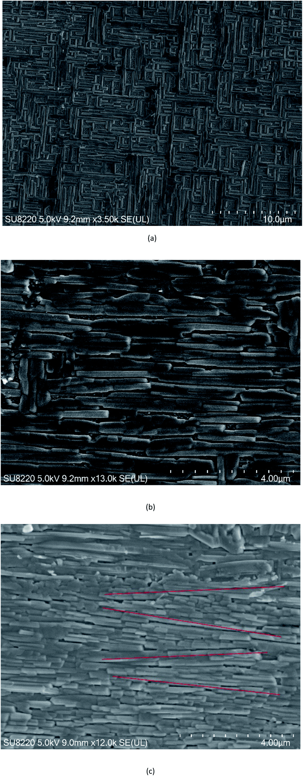 | ||
| Fig. 2 Typical SEM images of K0.3MoO3 thin films grown (a) on SrTiO3(100), (b) on SrTiO3(510), (c) on SrTiO3(110), respectively. The red line on SrTiO3(110) suggest the multidirectional growth of grains comparing with the unidirectional growth of grains on SrTiO3(510). | ||
In contrast, the K0.3MoO3 thin films exhibit only one preferential growth direction on the SrTiO3(510) substrate as shown in Fig. 2(b). The K0.3MoO3 (20) plane is parallel to the SrTiO3(510) plane and the interfacial match is shown in Fig. 3 with a 3.3% mismatch in one direction (the same as for the SrTiO3(100) substrate) and a 0.7% mismatch in the [50] direction. The majority of the rod-shaped grains are along [50] direction with few short grains along [001] direction.
 | ||
| Fig. 3 Schematic of the lattice match leading to K0.3MoO3 (20) and SrTiO3(510). The length of the K0.3MoO3 (20) lattice plane is calculated by cosine rule and the length of SrTiO3(510) is calculated by Pythagorean theorem. | ||
For growth of K0.3MoO3 on a SrTiO3(110) substrate there is a 3.3% mismatch in the [001] direction and 11.7% mismatch in the [10] direction; the resulting SEM image from such a film is shown in Fig. 2(c). The SrTiO3(110) plane does not have a square symmetry and does not match the K0.3MoO3 (20) plane as well as does the SrTiO3(510) plane. The SEM image for K0.3MoO3 grown on SrTiO3(110) is different from those from growth on SrTiO3 (100) and SrTiO3(510): the rod-shaped grains occur are found lying along several non-parallel directions (the red lines in Fig. 2(c) indicate the directions of the grains). We conclude that the most satisfactory epitaxial growth of K0.3MoO3 thin films occurs on a SrTiO3(510) substrate.
The topology of the K0.3MoO3 thin films was measured using AFM as presented in Fig. 4. The AFM images not only show similar grain structure as the SEM images in Fig. 2, but we can also determine the thickness of the grains from these images. We find that the thickness of the films on both SrTiO3(100) and SrTiO3(510) substrates is approximately 100 nm.
 | ||
| Fig. 4 Typical AFM images of K0.3MoO3 thin films grown (a) on SrTiO3(100), (b) on SrTiO3(510). | ||
3.2 Transport measurement
CDW phenomena tend to occur in chain compounds or layered structural materials where the CDW driven lattice distortion causes the metal to semiconductor transition. K0.3MoO3 has a chain structure with highly anisotropic charge transport: for single crystals, the resistivity (ρ) anisotropy ratio16 is about 1:30:1000 with most conducting direction17 ρ ∼ 5 × 10⁻⁶ to 5 × 10⁻⁵ Ω m. The experimental configuration for our 4-point probe measurement of the anisotropic resistivity as well as the metal to semiconductor transition in our films is shown in Fig. 5. First the resistivity was measured along one axis of the SrTiO3 substrate from 350 K to 90 K and then we rotated our substrate by 90° and measured along the other axis of the SrTiO3 substrate again from 350 K to 90 K.
 | ||
| Fig. 5 Schematic of measuring the temperature dependence of resistivity of K0.3MoO3 on different SrTiO3(100) axes by four-probe method. The gray squares represent the indium pads. | ||
The temperature dependence of the electrical resistivity of the K0.3MoO3 thin films is shown in Fig. 6. For SrTiO3(100) (Fig. 6(a)), the resistance does not show obvious variation along the [010] and [001] axes and this is anticipated from the square symmetry of the substrate. The resistivity can be calculated from  where R is the resistance, A is the cross-sectional area of the specimen,
 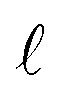 is the length of the sample. The resistance was R(T = 0 °C) = 340 Ω, the cross-sectional area is calculated by A = ad where a = 5 mm is the length of the substrate and d ∼ 100 nm is the thickness of the film,
 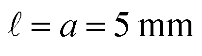 is also the length of the square substrate. The calculated ρ = 3.4 × 10⁻⁵ Ω m is consistent with the resistivity of the most conducting direction of single crystal K0.3MoO3. It is also observed that below about 180 K, the resistance increases much more rapidly than above 180 K. This result is consistent with the opening of a gap at EF due to the Peierls transition, as in single crystal K0.3MoO3.
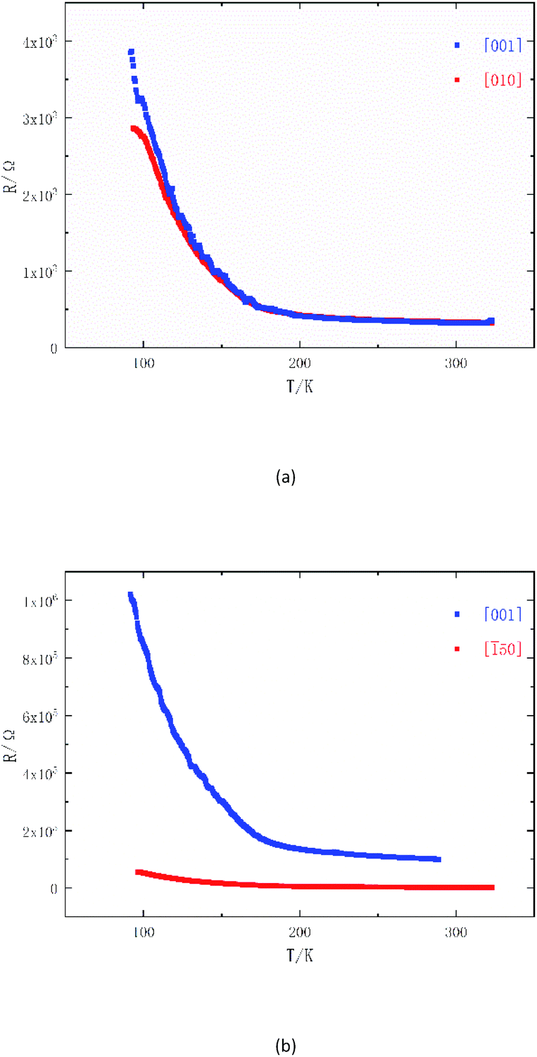 | ||
| Fig. 6 The temperature dependence of resistance for K0.3MoO3 thin films grown (a) on SrTiO3(100), (b) on SrTiO3(510). The blue and red curve represent different lattice axes. | ||
Fig. 6(b) shows the temperature dependence of the resistivity for blue bronze measuring along [001] and [50] axes of SrTiO3(510). Along [50], R(T = 0 °C) ∼ 2680 Ω, while along [001] R(T = 0 °C) ∼ 1 × 10⁵ Ω. The resistance ratio is about 1:37, similar to the anisotropy ratio in single crystals. From the resistance ratio in Fig. 6(b), we conclude that the second most conducting direction for blue bronze is also parallel to the substrate. The temperature dependence of the resistance for films grown on SrTiO3(510) is similar to those grown on SrTiO3(100) where the metal to semiconductor transition occurred around 180 K. The resistance R(T = 0 °C) for films grown on SrTiO3(510) along [50] is larger than the R(T = 0 °C) for those grown on SrTiO3(100); this may be due to variations in contact resistance, flatness of the film, or some unknown impurity.
4 Conclusions
We succeed in preparing high-quality crystalline K0.3MoO3 thin films by pulsed laser deposition on SrTiO3(100), SrTiO3(510) and SrTiO3(110) with thickness about 100 nm. The films were characterized by single crystal XRD, SEM, EDS, and AFM. Sample stoichiometry can be well controlled, and the morphology of the resulting films consists of K0.3MoO3 rods of variable sizes and depends on the substrate choice. The rods exhibit a square symmetry pattern on SrTiO3(100), a unidirectional pattern on SrTiO3(510), while on SrTiO3(110) the rods align along various directions. The temperature dependence of the electrical resistance reveals a very large anisotropy, and also a metal to semiconductor transition at about 180 K. Our preliminary results demonstrated the possibility of growing crystalline K0.3MoO3 thin films with controllable size and quality when the growth conditions are further carefully optimized. This may facilitate novel investigations of collective phenomena such as Peierls transition, periodic lattice distortions and CDWs in quasi-low dimensional solids.Conflicts of interest
There are no conflicts to declare.Acknowledgements
The authors acknowledge support from the Institute of Physics, Chinese Academy of Sciences for the PLD equipment.Notes and references
- C. Schlenker, J. Dumas, C. Escribe-Filippini and H. Guyot, in Low-Dimensional Electronic Properties of Molybdenum Bronzes and Oxides, Springer, 1989, pp. 159–257 Search PubMed.
- C. Schlenker, J. Dumas, C. Escribe-Filippini, H. Guyot, J. Marcus and G. Fourcaudot, Philos. Mag. B, 1985, 52, 643–667 CAS.
- M. Keizo, W. Yufeng, S. Yuki, T. Natarajan Rani, K. Kensuke, A. Sonachalam, T. Yusaku, Y. Harukazu and K. Reizo, Synth. Met., 2009, 159, 2397–2398 CrossRef.
- M. Greenblatt, Chem. Rev., 1988, 88, 31–53 CrossRef CAS.
- G. H. Bouchard Jr, J. H. Perlstein and M. J. Sienko, Inorg. Chem., 1967, 6, 1682–1685 CrossRef.
- J. Graham and A. Wadsley, Acta Crystallogr., 1966, 20, 93–100 CrossRef CAS.
- P. Monceau, N. Ong, A. M. Portis, A. Meerschaut and J. Rouxel, Phys. Rev. Lett., 1976, 37, 602 CrossRef CAS.
- M. Itkis, F. Y. Nad and P. Monceau, J. Phys.: Condens. Matter, 1990, 2, 8327 CrossRef CAS.
- A. Wold, W. Kunnmann, R. Arnott and A. Ferretti, Inorg. Chem., 1964, 3, 545–547 CrossRef CAS.
- R. Thorne, Phys. Rev. B: Condens. Matter Mater. Phys., 1992, 45, 5804 CrossRef CAS PubMed.
- D. Borodin, S. Zaitsev-Zotov and F. Y. Nad, Zh. Eksp. Teor. Fiz., 1987, 93, 1394–1409 CAS.
- T. Nishida and K. Eda, J. Nanopart. Res., 2018, 20, 27 CrossRef.
- H. Van Der Zant, O. Mantel, C. Dekker, J. Mooij and C. Træholt, Appl. Phys. Lett., 1996, 68, 3823–3825 CrossRef CAS.
- D. Dominko, D. Starešinić, K. Salamon, K. Biljaković, A. Tomeljak, H. Schäfer, T. Huber, J. Demsar, G. Socol and C. Ristoscu, J. Appl. Phys., 2011, 110, 014907 CrossRef.
- M. Schmidbauer, A. Kwasniewski and J. Schwarzkopf, Acta Crystallogr., Sect. B: Struct. Sci., 2012, 68, 8–14 CrossRef CAS PubMed.
- J. Pouget, S. Kagoshima, C. Schlenker and J. Marcus, J. Phys., Lett., 1983, 44, 113–120 CrossRef CAS.
- W. Fogle and J. H. Perlstein, Phys. Rev. B: Solid State, 1972, 6, 1402 CrossRef CAS.
| This journal is © The Royal Society of Chemistry 2022 |