 Open Access Article
Benzohexacene guide in accurate determination of field effect carrier mobilities in long acenes†
E. Bedel Pereiraa,
J. Bassalera,
H. Lavala,
J. Holecb,
R. Monfliera,
F. Mesnilgrentea,
L. Salvagnaca,
E. Darana,
B. Duployerd,
C. Tenailleau d,
A. Gourdon
 b,
A. Jancarikbc and
I. Séguy
 *a
*a
aLAAS-CNRS, Université de Toulouse, UPS, 31031 Toulouse, France. E-mail: iseguy@laas.fr
bCEMES-CNRS, 29 Rue J. Marvig, 31055 Toulouse, France
cCRPP, UMR CNRS 5031, Université de Bordeaux, 33600 Pessac, France
dCIRIMAT, Université de Toulouse, CNRS, Université Toulouse 3 – Paul Sabatier, 118 Route de Narbonne, 31062 Toulouse Cedex 9, France
First published on 23rd December 2021
Abstract
Oligoacenes are promising materials in the field of electronic devices since they exhibit high charge carrier mobility and more particularly as a semiconductor in thin film transistors. Herein, we investigate the field effect charge carrier mobility of benzohexacene, recently obtained by cheletropic decarbonylation at moderate temperature. Initially, high performance bottom contact organic thin-film transistors (OTFTs) were fabricated using tetracene to validate the fabrication process. For easier comparison, the geometries and channel sizes of the fabricated devices are the same for the two acenes. The charge transport in OTFTs being closely related to the organic thin film at the dielectric/organic semiconductor interface, the structural and morphological features of the thin films of both materials are therefore studied according to deposition conditions. Finally, by extracting relevant device parameters the benzohexacene based OTFT shows a four-probe contact-corrected hole mobility value of up to 0.2 cm2 V−1 s−1.
A. Introduction
Since the 1980s, intensive studies have been carried out in the organic electronics community to develop new semiconductors with appropriate electronic properties for their application in practical organic thin film transistors (OTFTs).1,2 Among these materials, n-acenes, which are polyaromatic planar organic compounds composed of linearly condensed benzene units, have been widely investigated, since they display one of the highest hole mobilities,3 such as tetracene (2.4 cm2 V−1 s−1 for its single crystals),4 tetraphenyltetracene commonly known as rubrene (>40 cm2 V−1 s−1 for its single crystals),5 and pentacene (>5.0 cm2 V−1 s−1 for its single crystals).6 Such impressive values of hole mobilities stem from large electronic coupling between adjacent molecules and low reorganization energy. In the case of n-acenes, the reorganization energy is decreasing with increasing number (n) of linearly fused benzene rings. Thus, long acenes are expected to be very good hole-transport semiconducting materials with mobility that increases as n increases. Although unsubstituted acenes are unipolar p-type semiconductors, their function can be tuned by their rational substitution into n-type or ambipolar semiconductors.7,8 Such a tunability is of great importance for designing next-generation electronic devices. Therefore, acenes are investigated for applications in organic light-emitting diodes (OLEDs),9 organic light-emitting transistors (OLETs),10 and organic thermoelectric generators,11 and they are also studied as molecular wires.12However, unsubstituted acenes are highly insoluble due to strong intermolecular π–π interactions, which hinder their chemical synthesis and purification at the same time. Moreover, acenes are known for their sensitivity to oxygen and in addition, acenes longer than pentacene dimerize in solution, even in very dilute solutions, which makes thin film and device fabrication unachievable. In 1996, A. R. Brown et al. demonstrated in their pioneering work the preparation of pentacene as the active component in OTFTs from its soluble and stable precursor, followed by the work carried out by M. Watanabe et al. in 1999.13,14 Since then, a variety of different proactive aceno-precursors have been prepared and their transformation to active acenes as semiconductors in organic field effect transistors (OFETs) has been investigated.15 The chemical step yielding the final acene from the precursor can be induced either by heating or by light. Until 2012, the pentacene was the longest unsubstituted acene integrated in OFETs, perhaps due to the deeply ingrained belief that longer acenes are too reactive to be implemented in electronic devices. In the seminal work of M. Watanabe et al.16 enough hexacene from its soluble and stable monocarbonyl precursor was synthesized and most importantly its good stability when integrated in OTFT devices was proved. From their transistor characteristics, they recorded a field effect mobility (μFE) of 4.28 cm2 V−1 s−1 for its single crystals16 and 0.076 cm2 V−1 s−1 for thin film mobility.17 In 2017, R. Einholz et al.18 obtained heptacene by thermal retro-cyclization of dimers; however, heptacene prepared by this strategy is unstable and converts back to the dimers which prevents any device fabrication. In 2019, A. Jancarik et al.19 have developed a general methodology for preparation of a variety of acenes longer than pentacene including heptacene from their stable and soluble carbonyl precursors at moderate temperatures. It is necessary to mention that heptacene prepared from the monocarbonyl precursor is stable for several months when stored under inert gas at room temperature thanks to different packing of heptacene molecules. First attempts to integrate heptacene (generated from monocarbonyl precursor) in OTFTs were reported very recently by T. Miyazaki et al. and showed promising μFE values.20 This powerful concept of having a stable and soluble proactive precursor, which can be transformed into acene on demand in quantitative yield and very high-quality, paves the way not only to the integration of promising novel molecules in organic devices, but it also allows for deepening more fundamental questions such as chemical topology, heteroatom doping, substitution or effect of open-shell configuration on OTFT performance. Furthermore, it will shed light on the validity of the above-mentioned law of charge mobility evolution with increasing n. As mentioned above, acenes longer than pentacene should allow high charge carrier mobilities due to the large electronic coupling between adjacent molecules and small reorganization energy. However, before pursuing to develop these materials to achieve promising mobilities, we must ensure that the mobility value obtained is accurate. Of course, the ideal system for investigation of electronic properties of organic semiconductors is to study them as an organic single crystal device. However, preparation of single crystals of many organic compounds can be in many cases extremely challenging, for reasons such as limited solubility, high reactivity, thermal stability, low volatility of compounds with high molecular weights, etc. Thus, they can be studied only in the thin film states which is bearing new hurdles.
In this study, we will discuss point by point all important parameters which have to be considered when studying transport properties, especially in thin film transistors. We investigate the charge carrier mobility of benzohexacene, derived from a bottom contact OTFT whose optimization, an important prerequisite, was conducted on tetracene based devices. Benzohexacene is at this moment one of the longest synthetized oligoacenes which can be processed either by spin-coating or vacuum evaporation. Herein, tetracene has been chosen as a reference material, for benchmark device preparation, since its field effect mobility is highly reported in the literature. However, the published values are widely dispersed. These deviations can be attributed to several factors such as the molecule arrangement in the film (molecular structure, supramolecular organization…), the film morphology, closely related to the deposition technique, the quality of the film interface with the dielectric layer and metal electrodes (material, defects, traps…) and the transistor architecture. Also, before studying new materials, it is of great importance to determine an optimized device and measurement method to be used rigorously. The need for formalized investigation procedures could be illustrated by the huge range of μFE values for tetracene thin films varying from 10−4 to 0.38 cm2. V−1 s−1, as reported in Table 1 (see ref. 28 and 24). These discrepancies are partly due to the chosen techniques for preparing organic thin films and dielectric surfaces, which may induce structural properties and therefore impact the transport for identical molecules.
| Ref. | Tetracene deposition method | Device structure | Dielectric layer | μFE (cm2 V−1 s−1) |
|---|---|---|---|---|
| a In these papers, the regime used for field effect mobility determination is not clearly defined.b Highest reported value. | ||||
| 21 | Sublimation, 0.5 Å s−1 | Bottom contact | SiO2 | μ = 1 × 10⁻²a |
| Substrate temperature: 15 °C, 25 °C | L = 10 μm | SiO2/OTS | μ = 0.12a | |
| W = 220 μm | ||||
| 22 | Neutral cluster beam, 5 Å s−1 | Top contact | SiO2 | μsat = 0.162 |
| L = 200, 660, 800, 1400 μm | SiO2/OTS | μsat = 0.252 | ||
| W = 500 μm | ||||
| 23 | Sublimation, deposition flux from 0.1 to 3 Å s−1 | Bottom contact | SiO2 | μsat = 0.13 |
| 24 | Sublimation, 4 nm min−1 | Top contact | SiO2 | μsat = 0.38b |
| L = 80 μm | ||||
| W = 500, 1000 μm | ||||
| 25 | Sublimation, 0.6 Å s−1-substrate temperature: 10 °C, 20 °C | Top contact | SiO2 | μsat = 1 × 10⁻⁴ |
| SiO2/AMS | μsat = 0.12 | |||
| 26 | Sublimation, 0.5 Å s−1 | Bottom contact | SiO2/OTS | μlin = 5 × 10⁻² |
| L = 5 μm | ||||
| W = 20 cm | ||||
| 27 | No details | Bottom contact | SiO2/OTS | μ = 4 × 10⁻³a |
| L = 15 μm | ||||
| W = 20 cm | ||||
| 28 | RESS (rapid expansion of supercritical solutions) | Top contact | SiO2/HMDS | μsat = 5.1 × 10⁻⁴ |
| L = 15 μm | ||||
| W = 2 mm | ||||
| 29 | Sublimation, 0.35 Å s−1 | Top contact | SiO2 | μsat = 1 × 10⁻² |
| L = 60, 80, 100 or 150 μm | SiO2/PS | μsat = 0.168 | ||
| W = 2 or 4 mm | SiO2/PARY C | μsat = 0.064 | ||
| SiO2/PMMA | μsat = 0.018 | |||
| SiO2/HMDS | μsat = 0.027 | |||
| This work | Sublimation, 0.4 Å s−1 | Bottom contact | SiO2 | μlin = 1.5 × 10⁻³ |
| L = 50 μm | SiO2/OTS | μlin = 0.12 | ||
| W = 1000 μm | ||||
This is particularly critical for linear acenes such as tetracene and pentacene which are known to exhibit polymorphic structures with substrate induced phases (SIP) related to the molecule/substrate interface and deposition process.29 The main important issue in accurate μFE determination is however related to OTFT fabrication and characterization since it is often the cause of μFE overestimation or underestimation. As mentioned above, this includes the transistor geometry (with constricted channel length lower than 10 μm for example) and errors made in the way of extracting μFE as argued by H. H. Choy et al.30 Among their guidelines for correct μFE determination, they pointed out that μFE must primarily be extracted from linear regime measurements (μlin), corresponding to the OTFT operating mode, with a specific focus on transfer characteristic linearity (linear and saturation mobility are clarified in the ESI†). If we look further in the results summarized in Table 1, it can be seen that in the literature, tetracene μFE is mostly obtained from saturation regime measurements (μsat).
In this paper we report a thorough investigation of benzohexacene field effect mobility considering both material and device parameters influencing μFE determination. Given that in oligoacenes charge carrier transport is known to be closely related to the crystalline quality of the organic active layer, the comparison of morphological, structural and electronic properties of tetracene and benzohexacene thin films will be discussed. Moreover, in order to assess accurate μFE values, we perform a detailed benzohexacene based OTFT study including four-probe devices. Using these devices, it is possible to determine a field effect mobility indicative of the intrinsic performances of the transistor without any influence from metal/organic semiconductor (OSC) series resistance.
B. Sample description
B.1. Architecture of OTFTs
Since the most studied oligoacene molecules like tetracene or pentacene are usually considered as hole transport materials, we choose a heavily doped n-type silicon wafer (ρ ∼ 10−3 Ω m) as the substrate for bottom gate thin film transistor fabrication. First, a 225 nm SiO2 thick film used as the gate dielectric was thermally grown on the silicon substrate with a measured insulator capacitance CSiO2 of 15.3 × 10⁻⁹ F cm−2, obtained at 10–100 kHz. Afterward, two photolithography and chemical etching steps were performed to obtain the pre-patterned OTFT electrodes (gate (G), source (S) and drain (D)). The first step consists in engraving the SiO2 layer in order to open bottom gate contacts (BG) constituted by the silicon substrate. The aim of the second one is to define source and drain patterns by Cr/Au (10 nm for chromium and 50 nm for gold) lift-off using 5 μm negative NLOF 2035 resist purchased from MicroChemicals.Fig. 1(a) and (b) display the structure and picture of a bottom-contact OTFT with a channel width (W) of 1000 μm and channel length (L) of 50 μm ± 1 μm after the organic layer deposition. For further field effect mobility investigations, a device type with different pre-patterned electrodes to obtain the so-called 4-probe OTFT was fabricated (Fig. 1(c)). The new substrates are constituted by two OTFTs and two 4-probe OTFTs. Each of them displays a W of 300 μm and L of 200 μm. For the 4-probe devices, the length between the two channel probes (D) is 80 μm (see the picture in Fig. 1(c)). Before the organic thin film preparation, a SiO2 surface decontamination was applied. All samples were cleaned by sonication in successive baths of acetone and isopropanol (10 min each), followed by a 5 min H2O2![[thin space (1/6-em)]](https://www.rsc.org/images/entities/char_2009.gif) :
:![[thin space (1/6-em)]](https://www.rsc.org/images/entities/char_2009.gif) H2SO4 (1
H2SO4 (1![[thin space (1/6-em)]](https://www.rsc.org/images/entities/char_2009.gif) :
:![[thin space (1/6-em)]](https://www.rsc.org/images/entities/char_2009.gif) 1) solution treatment and finally rinsed in deionized water and dried with nitrogen. In order to follow the SiO2/OSC interface influence on charge carrier mobility, some of the dielectric layers were modified by grafting an octadecyltrichlorosilane (OTS from Aldrich Co.) self-assembled monolayer (SAM). The grafting protocol consisted of substrate immersion in a mixture of 80 μL of OTS and 20 mL of chlorobenzene for 24 h, in a N2-filled glovebox. Organic thin films were deposited onto the substrates through a mask in order to pattern them (see Fig. 1(b) and (c)). Active organic layers were prepared during the same deposition batch on OTS treated and untreated dielectric surfaces in order to reduce run-to-run variations. Finally, the devices were encapsulated by a cover glass sealed with DELO KATIOBOND LP 655 (see the scheme in Fig. 1(a)).
1) solution treatment and finally rinsed in deionized water and dried with nitrogen. In order to follow the SiO2/OSC interface influence on charge carrier mobility, some of the dielectric layers were modified by grafting an octadecyltrichlorosilane (OTS from Aldrich Co.) self-assembled monolayer (SAM). The grafting protocol consisted of substrate immersion in a mixture of 80 μL of OTS and 20 mL of chlorobenzene for 24 h, in a N2-filled glovebox. Organic thin films were deposited onto the substrates through a mask in order to pattern them (see Fig. 1(b) and (c)). Active organic layers were prepared during the same deposition batch on OTS treated and untreated dielectric surfaces in order to reduce run-to-run variations. Finally, the devices were encapsulated by a cover glass sealed with DELO KATIOBOND LP 655 (see the scheme in Fig. 1(a)).
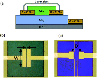 | ||
| Fig. 1 (a) Schematic representation of the bottom gate bottom contact OTFT and pictures of OTFTs with (b) tetracene 2-probe W = 1000 μm and L = 50 μm and (c) benzohexacene 4-probe devices D = 80 μm. | ||
The electrical device characterization was completed with commercial apparatus composed of a Karl Suss PA200 probe station and an Agilent 4142B (four source/measure units SMU). Measurements were performed using ground and high voltage SMUs with limit values up to 100 V and 100 mA for voltage and current source/drain and gate biases. For the 4-probe measurements, as five source/measure units SMU were needed, we used an Agilent 4156C. All electrical measurements were held in the dark, in air at room temperature. A careful examination of the way the electrode or dielectric preparation and OSC implementation modify the device behaviour has been made. This required the analysis of output (IDS–VDS) and transfer (IDS–VGS) transistor characteristics with in-depth electrical studies by extracting the following set of values from transfer characteristics: “off” current (Ioff), “on” current (Ion), threshold voltage (Vth), and device hysteresis.
B.2. Oligoacene deposition method
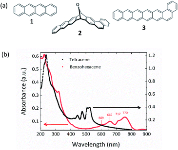
Fig. 2(a) shows the chemical structures of tetracene, benzohexacene precursor and benzohexacene (after decarbonylation) used in this study. Tetracene and benzohexacene precursor (see molecules 1 and 2 in Fig. 2(a)) were synthesized following established procedures.13 For thin film preparation by thermal evaporation molecules 1 and 2 are first disposed in Knudsen cells placed in a vacuum chamber at 2 × 10⁻⁷ mbar (Plassys MEB 550B). Organic thin films were then grown by sublimation at 80 °C and 200 °C for tetracene and benzohexacene respectively under high vacuum (2 × 10⁻⁷ mbar) at a low growth rate of ca. 0.4 Å s−1 with the substrate at room temperature. The thickness of the OSC film and deposition flux were controlled with a quartz vibrating thickness monitor placed near the samples.In such a case, for the longest acene, the precursor decarbonylation occurs during the evaporation process, before sublimation, while the powder is heated to 200 °C, directly leading to a benzohexacene thin film grown without any sample thermal post-treatment as described in previous work.19
The visible-near IR absorbance spectra, recorded on 75 nm tetracene and 90 nm thick benzohexacene films deposited onto quartz slides (using a Lambda 650 spectrometer in a two-beam configuration), are displayed in Fig. 2(b). The tetracene thin film exhibits an absorption spectrum comparable to that recorded by S. H. Lim et al.31 For the longest molecule, the obtained curve is similar to the one reported previously on spin-cast and thermally decarbonylated benzohexacene precursor layers, with the same four bands at 609, 665, 717 and 770 nm, demonstrating that benzohexacene (molecule 3, Fig. 2(a)) has been deposited onto the substrate.19
C. Results and discussion
It should be noted that one of the main parameters influencing charge transport in OTFTs is related to the organic thin film structure at the dielectric/OSC interface and especially to the supramolecular organization in the OSC layer. Indeed, for tetracene and pentacene which are linear acenes, a lot of papers point out the link between molecular arrangement due to thin film growth conditions (polymorphic structure, grain size…) and electronic material properties. So, in new long oligoacene field effect mobility study, it is of great importance to analyse the organic thin film morphological and structural properties.C.1. Morphological and structural oligoacene thin film properties
We have first performed AFM surface observation for tetracene and benzohexacene evaporated layers on SiO2/OTS substrates (during the same process as the OTFT fabrication), since OTS-grafted dielectric surfaces have been proved to improve hole transport in tetracene OTFTs.21,22 Sample topological properties were then studied by atomic force microscopy (AFM) using a Bruker Dimension ICON AFM in tapping mode. The two-dimensional AFM images are reported in Fig. 3(a) and (b). For tetracene films (Fig. 3(a)), the surface morphology consists in huge molecular stacks with faceted shapes, consistent with AFM observations already reported for tetracene obtained for low deposition flux.23 For the 50 nm (nominal thickness) thick layers, the film appears to be discontinuous (see Fig. S1 in the ESI†). However, the structures formed by tetracene molecules seem to be identical, evidencing a three-dimensional island growth mode. These islands consistent in shape and size could be attributed to the growth rate used for tetracene deposition (0.4 Å s−1) and to the OTS dielectric treatment used as observed by F. Cicoira et al.23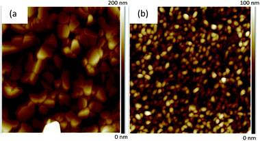 | ||
| Fig. 3 AFM tapping mode (a) 5 × 5 μm2 image of 75 nm tetracene and (b) 2 × 2 μm2 image of 50 nm benzohexacene films grown on SiO2/OTS substrates at a deposition flux of ca. 0.4 Å s−1. | ||
For the thickest 75 nm films (the ones used in devices), an improvement in substrate coverage is achieved, keeping the faceted shapes already observed on the thinnest film. For all those tetracene samples, the rms surface roughness extracted from AFM analysis software over a 5 × 5 μm2 area is significant, about 35 nm, approaching the nominal film thickness for the thinnest layer. By contrast (Fig. 3(b)), the 50 nm thick film of benzohexacene reveals a fairly homogeneous film, even for 20 nm thick layers (not shown here). It consists of a continuous surface composed of small grains leading to a rms roughness value of 14 nm, much lower than that obtained for tetracene.
The images shown in Fig. 3(a) and (b) highlight a very different morphology for the films of the two oligoacenes 1 and 3 processed under exactly the same conditions (same substrates, same vacuum in the chamber, and same evaporation rate). It is also interesting to notice here that for benzohexacene, we do not verify any island growth, as in 20 nm layers processed with low evaporation rate. We can presume that for this material, growing phases occur in a very different way from those described for shorter linear acene molecules such as tetracene and pentacene.32
In order to further compare the structural organization of these OSC thin-films, tetracene (75 nm) and benzohexacene (50 nm) on OTS-grafted SiO2 substrates have been characterized by X-ray diffraction. Structural characterization of films was performed in the Bragg–Brentano configuration using a Bruker D8 diffractometer equipped with a LynxEye 1D detector. Data were recorded using a Cu Kα wavelength radiation (40 kV, 40 mA) and collected at room temperature with a 0.02 step scan and 20 s per step. A nickel filter was used to eliminate the Kβ-ray and reduce fluorescence. Fig. 4(a) and (b) depict the diffraction patterns monitored in the range of 3° ≤ 2θ ≤ 35°. The obtained results demonstrate that both acene samples 1 and 3 exhibit a polycrystalline structure with a strong ordering due to the presence of harmonic peaks. Indeed, as for most of these organic molecules, the growth mode of these thin films is usually very particular. Here, XRD peaks corresponding to the (00l) reflections only are observed. Therefore, (ab) planes are parallel to the surface of the substrate and the distances between the layers correspond to the d00l spacings.
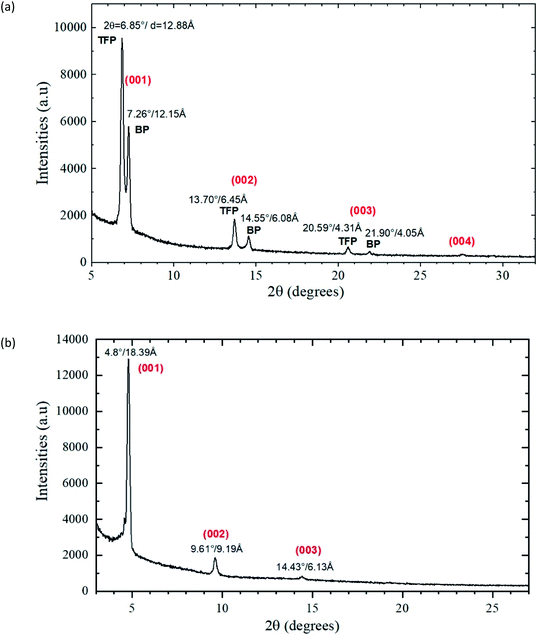 | ||
| Fig. 4 X-ray diffraction patterns of the (a) SiO2/OTS/tetracene (75 nm) and (b) SiO2/OTS/benzohexacene (50 nm) samples. | ||
For tetracene films, the X-ray diffraction allows for distinguishing two molecular arrangements evidenced by the presence of double peaks for each (00l) reflection (Fig. 4(a)). Such polymorphic structures have already been described for linear acenes and have been attributed to a surface-induced “thin film phase” (TFP) and a triclinic “bulk phase” (BP) for the first and second peaks of each pair of (00l) reflections respectively.33,34
Fig. 4(a) shows that the (001) lattice spacing is 12.15 Å for the bulk phase and 12.88 Å for the thin film. First, these values are in good agreement with the literature.35 Then, the different lattice spacing values indicate that the molecules are oriented differently from the normal of the substrate. Based on these d001 spacings and the length of the tetracene molecule of 13.53 Å,36 the tilt angle of this acene from the c-axis to the a-axis varied between 26° for the bulk phase and 17° for the thin film part. Since the TFP peak of the (001) reflection is much more intense than the BP one, this suggests that, in the tetracene films studied (on OTS treated SiO2 substrates), the highly oriented thin film phase extends over several molecular layers. It is noteworthy that for low flux evaporated tetracene (on untreated SiO2), as published by. Gompf et al.,37 a lower contribution of the TFP phase is expected. However, if relative amounts of TFP and BP phases are highly related to the deposition process (purity of the material source, flux, pressure, substrate temperature…), morphological analysis showed that substrate preparation, such as SAM treatment, also interferes in the tetracene growing process, resulting in likely different molecular arrangements.21–23,29 For benzohexacene, the XRD pattern clearly shows three main peaks at 4.8°, 9.6° and 14.4° in 2θ angles (see Fig. 4(b)). Most acenes being known to have a triclinic structure with two molecules per cell, we can thus assume that benzohexacene has the same crystalline organization. The observed multiple peaks can be fitted to a series of (00l) reflection lines, and the d001 lattice spacing is equal to 18.4 Å for the (001) series of planes. In comparison to the tetracene molecule-based XRD pattern discussed before, where a doublet of peaks was systematically observed, in the case of benzohexacene molecules a single series of peaks corresponding to the (001) reflections are observed, apart from a small intensity noticeable on the bottom left of the first reflection at 18.4 Å. In this case, most of the benzohexacene molecules were thus deposited with an orientation close to the perpendicular of the substrate. No other diffraction peaks corresponding to different (hkl) reflections are seen which means that only one structural organization exists for benzohexacene films. The length of this oligoacene being also bigger, as the d001 distance shows, we can suggest a much more tilted orientation of the molecules which would lead to a bulk phase with a single orientation.
For tetracene films, it was shown that the polymorph TFP and BP phase coexistence can be related to the organic material evaporation rate.32,37,38 Hence, in order to investigate the relationship between the structural organization and the deposition rate, we fabricated and characterized 50 nm-thick benzohexacene films with a growth rate of ca. 0.2, 0.4 and 2 Å s−1. No difference in each diffraction pattern is observed, indicating no structural change evidence by XRD (see Fig. S2†). Moreover, since growing studies of tetracene and pentacene polymorphs have demonstrated a thickness dependence of the TFB and BP phases, thinner and thicker benzohexacene films were examined. Structural characterization performed on 20 nm and 90 nm benzohexacene layers (see Fig. S3†) led to similar results to the ones already found for 50 nm thick layers, highlighting no effects of film thickness on the structural organization of this molecule. To conclude this comparison of the morphological and structural features of tetracene and benzohexacene films, we can state that the lack of a substrate induced phase in the longer acene layers seems to indicate a weaker impact (than the one observed during tetracene deposition) of molecule/substrate interaction in this mode of material growth.
C.2. Mobility determination from benzohexacene OTFT characteristics
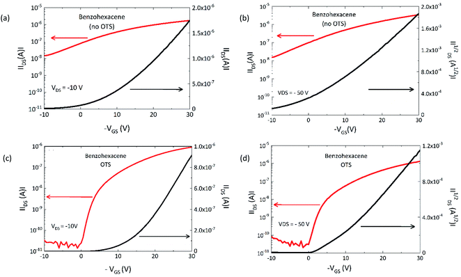
In this section, we investigated the transport properties of benzohexacene using the first device architecture developed (see Fig. 1b in Section B.1). In order to compare these devices with the tetracene ones (see ESI†), we focus this study on TFTs with a typical channel length L = 50 μm and width W = 1000 μm, operated at source-drain voltage up to −50 V. Two types of transistors were measured: without (no OTS) and with OTS pre-treatment (OTS) of the SiO2 surface. Their comparison will allow us to highlight the role of dielectric/OSC interfaces in the performance of the benzohexacene based-device. Fig. 5a and b illustrate the output room-temperature characteristics of the OTFT with a 50 nm-thick benzohexacene active layer. The drain current at negative gate bias saturates in the OTS-grafted OTFT following the standard FET behaviour for hole accumulation mode; for the no-OTS transistor, this saturation is less pronounced for VGS higher than −30 V (Fig. 5(a)).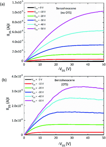 | ||
| Fig. 5 Output characteristics of the (a) no and (b) OTS-benzohexacene-based TFTs (W/L = 1000 μm/50 μm). | ||
However, the IDS values obtained are greater by a factor of three. For both devices, IDS–VGS plots are displayed in Fig. 6(a–d) in the linear and saturation regimes. The I–V measurements of all the devices considered do not show any hysteresis (not shown here). All the OTFT set of values extracted from transfer characteristics are summarized in Table 2. One can notice that, in comparison with tetracene (see ESI†), the transfer characteristics of the benzohexacene based transistors shift to a lower threshold voltage of −1 V and −1.5 V for OTS and no-OTS respectively. For 3, it should be noted that the difference between linear and saturation mobilities is relatively small, which is an indication of a good charge injection from the electrode to the active layer. Otherwise, we observe that the mobility obtained on the no-OTS device is comparatively slightly greater than that for the pre-treated SiO2 ones, both in the linear regime (0.022 cm2 V−1 s−1 (no OTS) and 0.017 cm2 V−1 s−1 (OTS)) and in the saturation regime (0.023 cm2 V−1 s−1 (no OTS) and 0.016 cm2 V−1 s−1 (OTS)). From this, we can argue, however, that for the same preparation condition, benzohexacene OTFT characteristics seem to be less influenced by dielectric SAM modification than tetracene based devices. For another long acene, hexacene, J. Han et al. also evidenced a low field effect hole mobility variation from 0.05 to 0.1 cm2 V−1 s−1 with OTS and polystyrene modified SiO2 surfaces respectively.39 These preliminary results tend to show that long non-substituted acenes (n ≥ 6 fused benzene rings) may exhibit a field effect mobility not strongly related to the dielectric surface as it is the case for tetracene and pentacene. In polycrystalline benzohexacene, the lack of the SIP structure noticed from XRD experiments could partly explain this behaviour.
| OTFT | Vth (V) | Ion/Ioff | μlin (cm2 V−1 s−1) | μsat (cm2 V−1 s−1) |
|---|---|---|---|---|
| Tetracene no OTS | −23 | 1.7 × 10³ | 0.0015 ± 4 × 10⁻⁵ | 0.0021 ± 4 × 10⁻⁵ |
| Tetracene OTS | −16 | 2.5 × 10⁶ | 0.119 ± 3 × 10⁻³ | 0.157 ± 3 × 10⁻² |
| Benzohexacene no OTS | −1.5 | 1.6 × 10⁴ | 0.0216 ± 6 × 10⁻⁴ | 0.0228 ± 7 × 10⁻⁴ |
| Benzohexacene OTS | −1 | 4.8 × 10⁶ | 0.017 ± 5 × 10⁻⁴ | 0.0158 ± 4 × 10⁻⁴ |
It is also interesting to notice that the results on hexacene (evaporated onto OTS-grafted SiO2) AFM topology published by J. Han et al. show a small grain morphology, very similar to the ones we have observed for benzohexacene thin films. In such samples, the hole transport might be mostly reduced by grain boundaries (see the AFM image in Fig. 3), resulting in traps located in the inter-grain region as it has been described for polycrystalline organic materials.40 In pentacene films, those traps have been identified as HOMO band-edge-fluctuations located at crystal-growth domain boundaries.41 However a significantly high μFE of 2.2 cm2 V−1 s−1 was recently published for heptacene grown layers exhibiting very small crystals with an estimated size of 17 nm.20 In order to achieve a better understanding of hole transport (with increasing n) in new n-acene molecules a thorough study of field effect mobility extraction is thus necessary. In the next section, we analyse the behaviour of μFE according to various parameters such as device geometry and operation mode.
C.3. Extensive charge carrier field effect mobility study in benzohexacene
From the previous results, we have shown that for the benzohexacene thin film structural and electronic properties remain unchanged with or without OTS dielectric modification. So, in order to complete the results described above, we limit the extensive mobility study to the devices without SiO2 treatment.First, for those devices, we have determined the reliability factor proposed by H. H. Choi et al.30 In the linear regime, the obtained value rlin is 73%. This factor highlights how much the mobility extracted from the OTFT data differs from the one obtained from an ideal transistor. If it is somehow impossible to reach ideal transistor characteristics with a material which does not behave like a single crystal semiconductor an extensive μFE study is needed to determine a reliable mobility value. So, we have examined the μFE variation with VGS for W/L 1000/50 μm transistors. Indeed, the equations used to extract field effect mobility (see ESI†) assume a constant charge carrier density (p), but, for some OTFTs, it has been shown that p could vary with applied bias, leading μFE to be gate voltage dependent. This variation is depicted in Fig. 7 with μlin and μsat obtained at VDS = −10 and −50 V respectively. It can be seen that μlin tends to saturate with VGS, indicating an almost constant μFE for VGS greater than – 15 V.
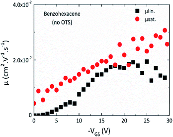 | ||
| Fig. 7 Mobility vs. VGS in linear (black, VDS = −10 V) and saturation (red, VDS = −50 V) regimes for the no-OTS benzohexacene based transistor with channel size W/L = 1000 μm/50 μm. | ||
In addition to supplementing the determination of hole mobility in benzohexacene thin films, we explored the consequence of the contact resistance effect on μFE. For long oligoacenes, molecules for which high μFE values are expected, the influence of contact resistance on device performances should increase significantly.42 Moreover, according to C. Liu et al.,43 gate dependence of contact resistance (RC) can result in possibly overestimated or underestimated μFE. One way used, to overcome the RC influence in μFE determination, is the four-probe method resulting in μ4p mobility which represents a contact-corrected linear mobility in the oligoacene.44 For this purpose, we have performed transfer characteristics measurements of four-gated benzohexacene OTFTs. The four-gated OTFTs have two additional small electrodes (35 μm width) placed on the sides of the channel as shown in the picture in Fig. 1c. The measurement of the voltage in the channel is performed independently using a high impedance electrometer to minimize the current in these probes. The equation used to get μ4p in the linear regime incorporating the four-gate geometric parameters and voltage V4p is expressed as
 | (1) |
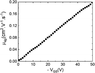 | ||
| Fig. 8 Four-probe mobility vs. VGS (calculated according to eqn (1)) in the linear regime (VDS = −10 V) for the no-OTS benzohexacene based transistor with channel size W/L = 300 μm/200 μm. | ||
From these results, it is therefore quite clear that to compare different oligoacene molecules with various HOMO/LUMO levels, thin film structures and morphologies leading to different contact resistance effects, μ4p should be more reliable than μFE reported in Section C.2. However, showing μ4p variations with VGS is still mandatory regarding charge transport in polycrystalline organic thin films. Based on these findings, it is for now difficult to draw a conclusion on charge mobility enhancement with the number of benzene units in the non-substituted longest oligoacenes. In fact, no reports of μ4p for devices based on thin films fabricated with those molecules are related in the literature.
D. Conclusions
In this paper, we presented the investigation of field effect hole mobility of a new acene, benzohexacene, and related it to its thin film morphological and structural properties. In contrast to shorter linear acenes like tetracene and pentacene, benzohexacene does not exhibit any polymorphic structures with surface induced phases. For this polycrystalline material, mobility limitations should be mostly due to its thin film morphology with crystal-growth domain boundaries acting as trap states. We have then further examined its hole field effect mobility extracted from linear and saturation regimes of bottom contact OTFTs and demonstrated that it was one order of magnitude lower than those obtained from four-probe gated transistors. Finally, we determine a benzohexacene four-probe hole mobility of 0.2 cm2 V−1 s−1 for VGS = −50 V. These results highlight that in order to determine the field-effect mobility of new molecules, great attention must be paid to the thin film structure and extraction method used especially for polycrystalline materials such as oligoacenes.Author contributions
Synthesis and characterization of the tetracene and benzohexacene molecules (AJ and JH), tetracene and benzohexacene film deposition and AFM characterization (IS and ED), XRD (BD and CT), device fabrication (FM, JB, HL, IS, and LS), OTFT characterization (EBP, JB, RM, and IS), four-gated OTFT characterization (RM, HL, and EBP), and project supervision (AG, IS, AJ, and EBP). All authors discussed the results and contributed to the preparation of the manuscript.Conflicts of interest
The authors declare no further conflicts of interest.Acknowledgements
This project has received financial support from the CNRS through the MITI interdisciplinary programs and “A. O. tremplin” “Matériaux et Application” programs from the University of Toulouse. Furthermore, the microfabrication procedure was partly supported by the French RENATECH network. The master internship of JB was supported by a FERMAT grant.References
- H. Sirringhaus, Adv. Mater., 2014, 26, 1319–1335 CrossRef CAS PubMed.
- Z. A. Lamport, H. F. Haneef, S. Anand, M. Waldrip and O. D. Jurchescu, J. Appl. Phys., 2018, 124, 071101 CrossRef.
- J. E. Anthony, Angew. Chem., Int. Ed., 2008, 47, 452–483 CrossRef CAS PubMed.
- C. Reese, W.-J. Chung, M.-M. Ling, M. Roberts and Z. Bao, Appl. Phys. Lett., 2006, 89, 202108 CrossRef.
- V. Podzorov, E. Menard, A. Borissov, V. Kiryukhin, J. A. Rogers and M. E. Gershenson, Phys. Rev. Lett., 2004, 93, 086602 CrossRef CAS PubMed.
- T. W. Kelley, P. F. Baude, C. Gerlach, D. E. Ender, D. Muyres, M. A. Haase, D. E. Vogel and S. D. Theiss, Chem. Mater., 2004, 16(23), 4413–4422 CrossRef CAS.
- K. J Baeg, J. Kim, D. Khim, M. Caironi, D.-Y. Kim, I.-K. You, J. R. Quinn, A. Facchetti and Y.-Y. Noh, ACS Appl. Mater. Interfaces, 2011, 3, 3205–3214 CrossRef PubMed.
- M. L. Tang, A. D. Reichardt, N. Miyaki, R. M. Stoltenberg and Z. Bao, J. Am. Chem. Soc., 2008, 130, 6064–6065 CrossRef CAS PubMed.
- H. D. Pham, H. Hu, F.-L. Wong, C.-S. Lee, W.-C. Chen, K. Feron, S. Manzhos, H. Wang, N. Motta, Y. M. Lam and P. Sonar, J. Mater. Chem. C, 2018, 6, 9017–9029 RSC.
- C. Zhang, P. Chen and W. Hu, Small, 2016, 12(10), 1252–1294 CrossRef CAS PubMed.
- H. Chen, M. Moser, S. Wang, C. Jellett, K. Thorley, G. T. Harrison, X. Jiao, M. Xiao, B. Purushothaman, M. Alsufyani, H. Bristow, S. De Wolf, N. Gasparini, A. Wadsworth, C. R. McNeill, H. Sirringhaus, S. Fabiano and I. McCulloch, J. Am. Chem. Soc., 2021, 143(1), 260–268 CrossRef CAS PubMed.
- H. J. Lee, S. J. Cho, H. Kang, X. He and H. J. Yoon, Small, 2021, 17(12), 2005711 CrossRef CAS PubMed.
- A. R. Brown, A. Pomp, D. M. de Leeuw, D. B. M. Klaassen and E. E. Having, J. Appl. Phys., 1996, 79, 2136 CrossRef CAS.
- P. T. Herwig and K. Müllen, Adv. Mater., 1999, 11, 480 CrossRef CAS.
- M. Watanabe, K.-Y. Chen, Y. J. Chang and T. J. Chow, Acc. Chem. Res., 2013, 46(7), 1606–1615 CrossRef CAS PubMed.
- M. Watanabe, Y. J. Chang, S. W. Liu, T. H. Chao, K. Goto, M. M. Islam, C. H. Yuan, Y. T. Tao, T. Shinmyozu and T. J. Chow, Nat. Chem., 2012, 4(7), 574–578 CrossRef CAS PubMed.
- M. Watanabe, T. Miyazaki, T. Matsushima, J. Matsuda, C.-T. Chein, M. Shibahara, C. Adachi, S.-S. Sun, T. J. Chow and T. Ishihara, RSC Adv., 2018, 8, 13259 RSC.
- R. Einholz, T. Fang, R. Berger, P. Grüninger, A. Früh, T. Chassé, R. F. Fink and H. F. Bettinger, J. Am. Chem. Soc., 2017, 139(12), 4435–4442 CrossRef CAS PubMed.
- A. Jancarik, G. Levet and A. Gourdon, Chem.–Eur. J., 2019, 25, 1–10 CrossRef PubMed.
- T. Miyazaki, M. Watanabe, T. Matsushima, C.-T. Chien, C. Adachi, S.-S. Sun, H. Furuta and T. J. Chow, Chem.–Eur. J., 2021, 27(41), 10677–10684 CrossRef CAS PubMed.
- D. J. Gundlach, J. A. Nichols, L. Zhou and T. N. Jackson, Appl. Phys. Lett., 2002, 80(6), 2925–2927 CrossRef CAS.
- Y. Jang, H. Seo, Y. Zhang and J. Choi, Org. Electron., 2009, 10, 222–227 CrossRef CAS.
- F. Cicoira, C. Santato, F. Dinelli, M. Murgia, M. A. Loi, F. Biscarini, R. Zamboni, P. Heremans and M. Muccini, Adv. Funct. Mater., 2005, 15, 375–380 CrossRef CAS.
- J. Shi, D. Jiang, J. R. Dutcher and X. Qin, J. Vac. Sci. Technol., B: Nanotechnol. Microelectron.: Mater., Process., Meas., Phenom., 2015, 33, 050604 Search PubMed.
- N. Moriguchi, T. Nishikawa, T. Anezaki, A. Unno, M. Tachibana and K. Kojima, Phys. B, 2006, 376–377, 276–279 CrossRef CAS.
- A. Hepp, H. Heil, W. Weise, M. Ahles, R. Schmechel and H. von Seggern, Phys. Rev. Lett., 2003, 91, 157406–157411 CrossRef PubMed.
- C. Santato, R. Capelli, M. A. Loi, M. Murgia, F. Cicoira, V. A. L. Roy, P. Stallinga, R. Zamboni, C. Rost, S. F. Karg and M. Muccini, Synth. Met., 2004, 146, 329–334 CrossRef CAS.
- T. Fujii, Y. Takahashi and H. Uchida, Appl. Phys. Express, 2015, 8, 035504 CrossRef CAS.
- J. Wünsche, G. Tarabella, S. Bertolazzi, M. Bocoum, N. Coppedè, L. Barba, G. Arrighetti, L. Lutterotti, S. Iannotta, F. Cicoira and C. Santato, J. Mater. Chem. C, 2013, 1, 967–976 RSC.
- H. H. Choi, K. Cho, C. D. Frisbie, H. Sirringhaus and V. Podzorov, Nat. Mater., 2017, 17, 2–7 CrossRef PubMed.
- S. H. Lim, T. G. Bjorklund, F. C. Spano and C. J. Bardeen, Phys. Rev. Lett., 2004, 92, 107402 CrossRef PubMed.
- R. K. Nahm and J. R. Engstrom, J. Chem. Phys., 2017, 146, 052815 CrossRef CAS PubMed.
- S. Milita, C. Santato and F. Cicoira, Appl. Surf. Sci., 2006, 252, 8022–8027 CrossRef CAS.
- A. C. Mayer, A. Kazimirov and G. Malliaras, Phys. Rev. Lett., 2006, 97, 105503 CrossRef PubMed.
- L. Pithan, D. Nabok, C. Cocchi, P. Beyer, G. Duva, J. Simbrunner, J. Rawle, C. Nicklin, P. Schäfer, C. Draxl, F. Schreiber and S. Kowarik, J. Chem. Phys., 2018, 149, 144701 CrossRef PubMed.
- R. B. Campbell and J. Monteath Robertson, Acta Crystallogr., Sect. A: Cryst. Phys., Diffr., Theor. Gen. Crystallogr., 1962, 15, 289–290 CrossRef CAS.
- B. Gompf, D. Faltermeier, C. Redling, M. Dressel and J. Pflaum, Eur. Phys. J. E, 2008, 27, 421–424 CrossRef CAS PubMed.
- S. Milita, M. Servidori, F. Cicoira, C. Santato and A. Pifferi, Nucl. Instrum. Methods Phys. Res., Sect. B, 2006, 246, 101–105 CrossRef CAS.
- J. Han, X. Liu, Y. Li, Z. Lou, M. Yi, H. Kong and J. Luo, Org. Chem. Front., 2019, 6, 2839 RSC.
- G. Horowitz, Adv. Funct. Mater., 2003, 13, 53–60 CrossRef CAS.
- R. Matsubara, Y. Sakai, T. Nomura, M. Sakai, K. Kudo, Y. Majima, D. Knipp and M. Nakamura, J. Appl. Phys., 2015, 118, 175502 CrossRef.
- G. Hrowitz, J. Mater. Res., 2004, 19, 1946 CrossRef.
- C. Liu, G. Li, R. Di Pietro, J. Huang, Y. Y. Noh, X. Liu and T. Minari, Phys. Rev. Appl., 2017, 8, 034020 CrossRef.
- C.-Y. Chen and J. Kanicki, IEEE Electron Device Lett., 1997, 18, 340–342 CAS.
- G. Horowitz, R. Hajlaoui, D. Fichou and A. El Kassmi, J. Phys. D: Appl. Phys., 1999, 85, 3202 CAS.
- G. Horowitz, M. E. Hajlaoui and R. Hajlaoui, J. Phys. D: Appl. Phys., 2000, 87, 4456 CAS.
Footnote |
| † Electronic supplementary information (ESI) available. See DOI: 10.1039/d1ra07808a |
| This journal is © The Royal Society of Chemistry 2022 |

