DOI:
10.1039/D1RA07712K
(Paper)
RSC Adv., 2022,
12, 4113-4119
Thin film encapsulation for quantum dot light-emitting diodes using a-SiNx:H/SiOxNy/hybrid SiOx barriers
Received
19th October 2021
, Accepted 29th December 2021
First published on 2nd February 2022
Abstract
A facile thin film encapsulation (TFE) method having a triple-layered structure of a-SiNx:H/SiOxNy/hybrid SiOx (ASH) on QD-LEDs was performed utilizing both reproducible plasma-enhanced chemical vapor deposition (PECVD) and simple dip-coating processes without adopting atomic layer deposition (ALD). The ASH films fabricated on a polyethylene terephthalate (PET) substrate show a high average transmittance of 88.80% in the spectral range of 400–700 nm and a water vapor transmission rate (WVTR) value of 7.3 × 10⁻⁴ g per m2 per day. The measured time to reach 50% of the initial luminance (T50) at initial luminance values of 500, 1000, and 2000 cd m−2 was 711.6, 287.7, and 78.6 h, respectively, and the extrapolated T50 at 100 cd m−2 is estimated to be approximately 9804 h, which is comparable to that of the 12![[thin space (1/6-em)]](https://www.rsc.org/images/entities/char_2009.gif) 112 h for glass lid-encapsulated QD-LEDs. This result demonstrates that TFE with the ASH films has the potential to overcome the conventional drawbacks of glass lid encapsulation.
112 h for glass lid-encapsulated QD-LEDs. This result demonstrates that TFE with the ASH films has the potential to overcome the conventional drawbacks of glass lid encapsulation.
1. Introduction
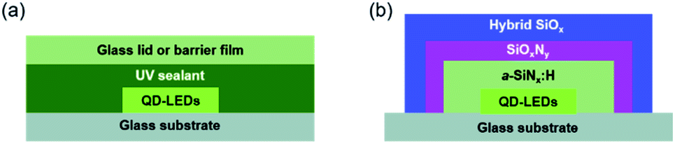
Organic electronic devices such as quantum dot light-emitting diodes (QD-LEDs), organic light-emitting diodes (OLEDs), organic photovoltaics (OPV), and perovskite solar cells have attracted much attention for application in large scale and flexible optoelectronic devices due to their high flexibility, low cost, easy fabrication, and light weight.1–6 Among these devices, QD-LEDs have been extensively explored for display applications due to their size-tunable emission wavelength, high quantum yield, narrow emission peaks, and low-cost manufacturing.7–9 Despite these advantages, QD-LEDs have a major drawback, similar to OLEDs: their performance deteriorates rapidly in atmospheric environments. It is well known that QD-LED and OLED materials are very vulnerable to moisture and oxygen.10,11 To meet the requirements, encapsulation should achieve a water vapor transmission rate (WVTR) and oxygen transmission rate (OTR) of less than 1 × 10⁻⁶ g per m2 per day and 1 × 10⁻⁵ cm3 per m2 day, respectively.12–14 As shown in Fig. 1(a), conventional encapsulation with a glass lid or barrier foil is known as stable encapsulation barrier technology, but limitations such as edge permeation through the sealant limit upscaling of the device area, make handling difficult, and cause a lack of flexibility.15,16 Many types of encapsulation methods have been studied to solve this problem. Thin film encapsulation (TFE) is considered a potential candidate because it blocks moisture and oxygen that can penetrate from the edge, and unlike existing glass lids or barrier foil, it does not use an adhesive, so contamination that may be caused by the adhesive can be avoided. In addition, TFE is flexible, so it is easy to apply in bendable, rollable, and foldable displays.16 Several studies related to TFEs have been carried out, such as inorganic single layers of SiNx, Al2O3, and SiO2 by PECVD, ALD, and sputtering.17–20 Among them, the ALD method is considered a promising candidate for achieving a dense inorganic layer such as Al2O3 because ALD produces very thin, dense, and uniform films at low temperature (<100 °C) via control of the thickness and reaction cycles. More recent research has reported that ultrahigh barrier films, defined as films having a WVTR lower than ∼10−6 g per m2 per day, have been successfully fabricated by adopting ALD.21–27 The ALD process is, however, expensive due to the use of a vacuum process and is also unproductive due to a quite low deposition rate and high precursor gas usage and energy.28,29 Thus, we previously reported a facile fabrication method for ultrahigh barrier films with a WVTR value of 2 × 10⁻⁶ g per m2 per day with hydrogenated amorphous silicon nitride (a-SiNx:H)/silicon oxynitride (SiOxNy)/hybrid silicon oxide (h-SiOx) multilayer barrier films.30,31 In this study, a triple layered structure of a-SiNx:H/SiOxNy/hybrid SiOx (ASH) on QD-LEDs, as shown in Fig. 1(b), was fabricated as a thin film encapsulation for QD-LEDs using both PECVD and a simple dip-coating method. An approximately 400 nm thick amorphous hydrogenated silicon nitride (a-SiNx:H) film was directly deposited on the QD-LED device by plasma-assisted chemical vapor deposition (PECVD). Organic modified silica (ORMOSIL) sols were sequentially coated on a-SiNx:H thin films and annealed in an oven at 120 °C for 10 h for the formation of dense silicon oxynitride (about 8 nm thickness) at the interface between the a-SiNx:H film and the hybrid SiOx film. The total thickness of the ASH films was about 1 μm. In the ASH films, the interlayer SiOxNy thin film has a very high density of 3.32 g cm−3 and plays an important role in preventing moisture and oxygen penetration. At an initial luminance of 100 cd m−2, the estimated time to reach 50% of the initial luminance (T50) of encapsulated QD-LEDs of glass/ITO/PEDOT:PSS/PVK/CdSe-ZnS/ZnO/Al with the ASH films was 9840 h, and the results were compared with those encapsulated with a glass lid.
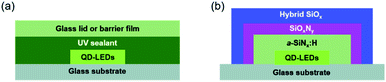 |
| | Fig. 1 (a) Schematic of conventional glass lid encapsulated QD-LEDs and (b) the ASH films encapsulated QD-LEDs. | |
2. Experimental
2.1. Fabrication of a-SiNx:H/SiOxNy/hybrid SiOx high barrier film
The a-SiNx:H/SiOxNy/hybrid SiOx hybrid barrier films were prepared on 125 μm thick PET (V7610, SKC) substrates of 210 mm × 297 mm. The deposition of the a-SiNx:H layer was carried out in a parallel plate capacitively coupled radio-frequency (13.56 MHz) discharge plasma-enhanced chemical vapor deposition (PECVD) system (JH Tech Co., Ltd.). The base pressure was kept at 40 mTorr by a rotary and booster pump. The precursor gas for the deposition of the a-SiNx:H films was a mixture of silane (SiH4), ammonia (NH3), and nitrogen (N2) as a dilute gas at an optimized flowing ratio of 25:100:380 cm3 min−1. The deposition was performed at 120 °C for 8 min to obtain 400 nm thick a-SiNx:H films. Next, a SiOxNy/hybrid SiOx layer was formed on the a-SiNx:H layer by dip-coating and post-deposition annealing of an ORMOSIL sol (SOH 204-4, Changsung Nanotech Co., Ltd.) coating. Prior to dip-coating, oxygen plasma treatment was performed and the ORMOSIL sol was coated on the a-SiNx:H surface at a withdrawal speed of 3 mm s−1 with a dip coater (EF-4200, E-Flex, Korea) after an immersion time of 5 min, and the samples were then annealed at 120 °C for 10 h in an oven (FO600M, JEIO Tech, Korea). During this annealing process, the ORMOSIL sol reacted with the a-SiNx:H layer by penetrating and flattening it, forming a ca. 8 nm thick interfacial SiOxNy layer between a-SiNx:H and hybrid SiOx.
2.2. QD-LEDs fabrication and thin film encapsulation
The multilayer-structured QD-LED was fabricated layer-by-layer using a spin-casting method and a vacuum evaporation method. The substrates were ultrasonically cleaned using acetone, ethanol, and deionized water for 15 min and then treated with O2 plasma for 1 min. PEDOT:PSS (Heraeus, Clevios PH-1000) was spin-coated on the ITO glass substrates at 4000 rpm for 40 s and baked at 130 °C for 30 min onto the ITO/glass as a hole injection layer (HIL). The ITO glass substrates were transferred to a nitrogen glove box where the remaining fabrication steps were carried out. PVK (Sigma-Aldrich, Mn 25000–50000) was spin-coated on top of PEDOT:PSS layer at 5000 rpm for 40 s and annealed at 130 °C for 30 min, followed by spin-coating of a green QD (CdSe-ZnS) layer on the top of it and subsequent annealing at 90 °C for 30 min. Then, ETL of ZnO NPs was deposited on the QD layer using spin-coating at 3000 rpm for 40 s and baked at 130 °C for 30 min. Finally, an Al cathode film (120 nm) was deposited by thermal evaporation through a patterned shadow mask. The following step was thin film encapsulation. We deposited the a-SiNx:H layer first using the PECVD method, and the hybrid SiOx was dip-coated. Fig. 1 shows the schematic diagram of the final structure of the device. Glass lid encapsulation was executed using a UV-curable sealant (XNR5570-Ba, Nagase ChemteX, Japan) as a reference.
2.3. Characterization and measurement
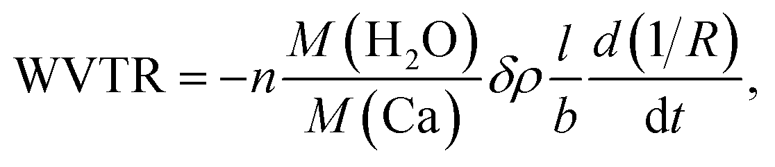
The microstructure and thickness of the ASH film-encapsulated QD-LEDs were characterized by TEM (Titan TM 80-300, FEI, USA). Optical transmittance was measured with an ultraviolet-visible (UV-vis) spectrometer (Lambda 18 UV/vis/NIR spectrometer, PerkinElmer, USA). The refractive index (n) of the a-SiNx:H, SiOxNy, and SiOx films was measured by spectroscopic ellipsometry (RC2-XF, J.A. Wollam Co., USA). To obtain the WVTR value, the calcium (Ca) test was conducted. First, 100 nm aluminum (Al) was deposited by thermal evaporation on the glass substrate (2.5 cm × 2.5 cm). Then, 100 nm of Ca pad was deposited by thermal evaporation. The area of the Ca pad on the glass substrate is 1.5 cm2. The Ca pad was sealed with bare PET, PET/a-SiNx:H and PET/ASH films using a UV-curable sealant (XNR5570-Ba, Nagase ChemteX, Japan). All encapsulation processes were carried out in a nitrogen-filled glove box. Finally, during degradation of the Ca pad in the climate chamber at 38 °C and 85% RH, the resistance of the sensor was monitored in situ using the four-point probe system (Keithley 2400, USA). The I–V–L characteristics of the QD-LED device were measured using a Spectra Scan PR-670 spectroradiometer and a Keithley 2400 source-measure unit. Operational lifetime test of the unencapsulated QD-LEDs and QD-LED encapsulated with the a-SiNx:H film, the ASH films, and glass lid were measured by a McScience OLED Lifetime Test System (M6000 PLUS) at ambient conditions (temperature, 20–25 °C; relative humidity, 30–70%).
3. Results and discussion
Optical transparency is very important for a barrier film because most applications require a transmittance of 90% in the visible light range. Therefore, the optical transmittance of the ASH barrier films was measured in the visible wavelength range of 400–700 nm based on air. As seen in Fig. 2(a), the PET/ASH barrier films show an average transmittance (Tavg) value of 88.80% in the range of 400–700 nm, which is comparable to those of bare PET (88.39%) and PET/a-SiNx:H film (84.51%). As shown in the inset in Fig. 2(a), the logo image is clearly visible through the PET/ASH films. The measured refractive indices for a-SiNx:H (n1 = 1.76), SiOxNy (n2 = 1.65), and hybrid SiOx (n3 = 1.48) show gradual increase from the top layer (hybrid SiOx) to the bottom layer (a-SiNx:H).30 Therefore, such a gradient refractive index plays a major role in reducing the loss of Fresnel reflection and thus increases the transmittance. The barrier properties of the PET/ASH films were characterized by the calcium corrosion test (Ca test). The Ca test uses a resistance change according to the degree of Ca corrosion.14,32 Fig. 2(b) shows the real-time normalized conductance changes in the Ca films with bare PET, PET/a-SiNx:H, and the PET/ASH film over time under storage conditions of temperature at 38 °C and relative humidity (RH) at 85%. The schematic cross-sectional view of the Ca sensor is also provided in Fig. 2(b) inset. The WVTR value was estimated using eqn (1).32| |
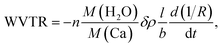 | (1) |
where n is the number of water molecules per calcium atom, M is the molar mass, δ is the calcium density, ρ is the calcium resistivity, l is the length of the calcium layer, b is the width of the calcium layer, R is the resistance of the calcium layer, and t is the time. The rate of change in the conductance, d(1/R)/dt, can be extracted from the slope of the calcium test plot. According to Fig. 2(c), the calculated WVTR values of bare PET, PET/a-SiNx:H, and the PET/ASH films through the Ca test are 3.4, 4.5 × 10⁻², and 7.3 × 10⁻⁴ g per m2 per day, respectively. The improved barrier properties of the ASH films are attributed to the formation of dense SiOxNy between a-SiNx:H and hybrid SiOx that effectively passivates the leakage channels and elongates the water molecular diffusion length by the formation of tortuous paths. In our previous study,30 the density for the a-SiNx:H, SiOxNy, and hybrid SiOx layers were obtained from the XRR analysis. From the XRR analysis, the density of the SiOxNy layer was estimated as 3.32 g cm−3, which is higher than the d = 1.3 g cm−3 of hybrid SiOx and d = 2.28–2.33 g cm−3 of a-SiNx:H. The mechanism of the formation of dense SiOxNy is discussed as follows. Hydroxyl (–OH) groups are induced on the oxygen plasma-treated a-SiNx:H surface through hydrogen bonds and then react with other –OH groups present on the surface of the hybrid SiOx film by hydrolysis. A condensation reaction subsequently takes place between the hybrid SiOx and a-SiNx:H in the annealing step, resulting in the formation of the SiOxNy layer. The SiOxNy formed by O–Si–N networks can be deduced to be denser than porous hybrid SiOx and a-SiNx:H containing abundant hydrogen. This is because the water molecules formed by hydrogen bonds and the polymer chain derived from the hybrid SiOx layer diffuse out from the SiOxNy layer during the 10 h of the critical annealing step. We fabricated green QD-LEDs consisting of patterned ITO, PEDOT:PSS as a hole injection layer (HIL), PVK layer as a hole transport layer (HTL), CdSe-ZnS QDs as the emission layer (EML), ZnO as the electron transport layer (ETL), and Al as the cathode. PEDOT:PSS/PVK/CdSe-ZnS QDs/ZnO are fabricated on a glass/ITO substrate by spin-coating. The Al layer is deposited by thermal evaporation. Afterwards, thin film encapsulation using the ASH films was carried out over the Al top layer. Fig. 3(a) presents cross-sectional TEM images of the ASH barrier layer-encapsulated QD-LED devices. The ITO (150 nm)/PEDOT:PSS/PVK (45 nm)/CdSe-ZnS (30 nm)/ZnO (50 nm)/Al (100 nm) of the QD-LEDs and the ASH films consisting of a-SiNx:H (398 nm) and hybrid SiOx (527 nm) are obviously visible. In the magnified view of the ASH layers (Fig. 3(b)), the formation of an interfacial layer of SiOxNy with 7.81 nm thickness is clearly identified between a-SiNx:H and hybrid SiOx. Fig. 3(c) presents real images of the QD-LED devices encapsulated with the a-SiNx:H film, the ASH films, and glass lid, respectively. In the photograph, the red-dashed square region indicates the area of the thin film encapsulation fabricated on the QD-LED devices. As shown Fig. 3(c), the TFE process with the ASH films appears to have no damage to the QD-LEDs. To evaluate the performance of the QD-LEDs encapsulated with the ASH layers, we measured their electrical characteristics before and after the encapsulation process. Fig. 4 shows the change of current density (mA cm−2) and luminance (cd m−2) of the QD-LEDs as a function of the applied forward bias. Except for the QD-LEDs with no encapsulation, the electrical behavior of the current density and luminance of the QD-LEDs show a similar pattern. The turn-on voltages of all QD-LED devices, including the unencapsulated QD-LEDs, were all identical at about 4 V. The maximum luminance was 13530 cd m−2 for the ASH film-encapsulated QD-LEDs and those of the unencapsulated, the a-SiNx:H film-encapsulated, and glass lid QD-LEDs were 10589, 13650, and 15910 cd m−2, respectively. Based on these results, the luminance of the QD-LEDs encapsulated by the ASH films is 85% that of QD-LEDs with a glass lid, which proves that the ASH-TFE process has a little influence on the electroluminescence of QD-LEDs. In order to investigate the long-term stability of the QD-LEDs, we performed an operational lifetime test of unencapsulated, a-SiNx:H film, ASH film, and glass lid-encapsulated QD-LEDs at a current corresponding to an initial luminance of about 500, 1000, and 2000 cd m−2. Fig. 5 shows the change of luminance (cd m−2) of the QD-LEDs versus the exposure time in an operational lifetime test. The lifetime of the unencapsulated QD-LEDs and those encapsulated with a-SiNx:H degraded rapidly when exposed to air. On the other hand, the ASH films and glass lid encapsulated QD-LEDs show device lifetimes (T50) of 711.6, 287.7, and 78.6 h at initial luminance values of 500, 1000, and 2000 cd m−2 and 1234.2, 411.6, and 145.6 h at initial luminance values of 510, 1350, and 2500 cd m−2, respectively. In addition, we estimated the T50 value at 100 cd m−2 using the empirical formula (eqn (2))33 and the raw data shown in Fig. 5.| | |
L0n × T50 = constant,
| (2) |
where L0 is the initial luminance and n is the acceleration factor.
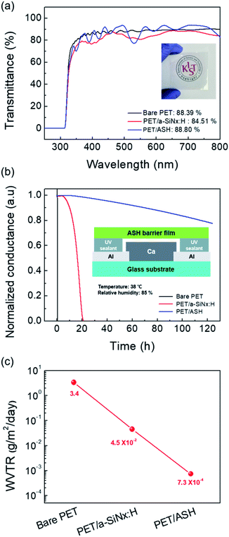 |
| | Fig. 2 (a) Optical transmittance spectra of the bare PET substrate, PET/a-SiNx:H film, and PET/ASH film. The inset shows photograph of the KIST logo under a PET/ASH barrier. (b) The normalized conductance curve of bare PET, PET/a-SiNx:H film, and PET/ASH film. The inset displays a schematic of the Ca sensor. (c) The calculated WVTR values of bare PET, PET/a-SiNx:H film and PET/ASH film from the Ca test. | |
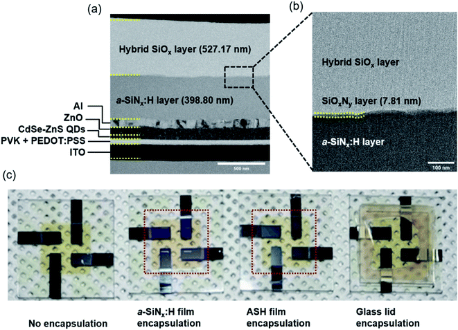 |
| | Fig. 3 (a) Cross-sectional TEM images of encapsulated QD-LEDs with the ASH film and (b) the magnified view of the ASH layer. (c) Photograph of QD-LEDs without encapsulation and encapsulated with the a-SiNx:H film, the ASH film, and glass lid. | |
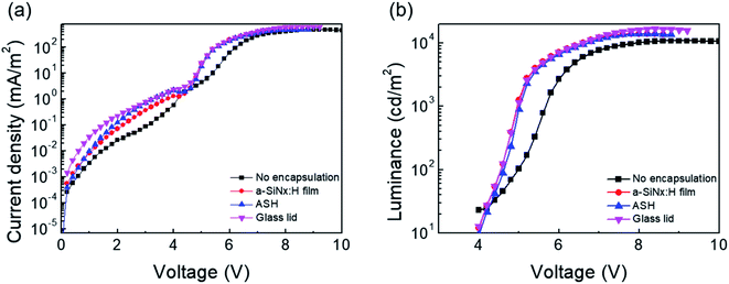 |
| | Fig. 4 (a) Luminance–voltage characteristic curve and (b) current density–voltage characteristic curve of the QD-LEDs without encapsulation and QD-LEDs encapsulated with the a-SiNx:H film, the ASH films, and glass lid. | |
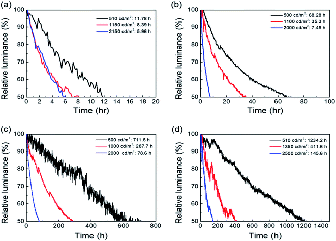 |
| | Fig. 5 (a) Operational lifetimes of the QD-LEDs without encapsulation, and (b) encapsulated QD-LEDs with the a-SiNx:H film, (c) the ASH films, and (d) glass lid. | |
As shown Fig. 6(a), the estimated T50 at 100 cd m−2 for unencapsulated and a-SiNx:H-encapsulated QD-LEDs by extrapolation was also calculated to be less than 1000 h. On the other hand, the ASH layer-encapsulated QD-LEDs show quite a long estimated T50 of 9804 h, which is comparable to that of the 12112 h for glass lid-encapsulated QD-LEDs. As shown in Fig. 6(b), the ASH film-encapsulated QD-LEDs were successfully and endurably operated even in water. This result demonstrates that the ASH-TFE process has the potential to overcome the conventional drawbacks of glass lid encapsulation.
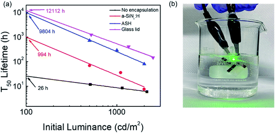 |
| | Fig. 6 (a) The estimated T50 of the QD-LEDs without encapsulation, and encapsulated QD-LEDs with the a-SiNx:H film, the ASH film, and glass lid. (b) Photograph of the encapsulated QD-LEDs with the ASH film immersed in water. | |
4. Conclusion
We encapsulated a-SiNx:H/SiOxNy/hybrid SiOx (ASH) barriers on QD-LEDs without physical and chemical damage using consecutive facile and very reproducible PECVD and simple dip-coating processes. In the ASH films, the SiOxNy thin film between a-SiNx:H and hybrid SiOx has a very high density of 3.32 g cm−3 and was found to be the most effective layer for preventing moisture permeation in terms of the barrier properties. In a spectral range of 400–700 nm, the ASH barrier films have an average transmittance of 88.80%. The WVTR value was measured to be 7.3 × 10⁻⁴ g per m2 per day by the electrical Ca test. Electrical performance and operational lifetime tests were performed to determine whether thin film encapsulation could be applied to the QD-LEDs. The ASH-encapsulated QD-LEDs behaved identically before and after the ASH-TFE process. The T50 values measured at the initial luminance values of 500, 1000, and 2000 cd m−2 are 711.6, 287.7, and 78.6 h, respectively, and the extrapolated T50 at 100 cd m−2 is estimated to be approximately 10000 h. This result demonstrates that ASH-TFE has the potential to overcome the conventional drawbacks of glass lid encapsulation. We expect that our proposed ASH-TEF will overcome the shortcomings of the existing glass lid encapsulation and be utilized as an encapsulation technology that can be applied to organic electronic devices.
Conflicts of interest
There are no conflicts to declare.
Acknowledgements
This work was partially supported by the Materials, Components & Equipments Research Program funded by the Gyeonggi Province (AICT11T2) and the KIST Institutional Program.
Notes and references
- Y.-F. Liu, J. Feng, Y.-G. Bi, D. Yin and H.-B. Sun, Adv. Mater. Technol., 2019, 4, 1800371 CrossRef.
- W. H. Koo, S. M. Jeong, F. Araoka, K. Ishikawa, S. Nishimura, T. Toyooka and H. Takezoe, Nat. Photonics, 2010, 4, 222–226 CrossRef CAS.
- K. Goushi, K. Yoshida, K. Sato and C. Adachi, Nat. Photonics, 2012, 6, 253–258 CrossRef CAS.
- H. Uoyama, K. Goushi, K. Shizu, H. Nomura and C. Adachi, Nature, 2012, 492, 234–238 CrossRef CAS PubMed.
- O. Inganas, Adv. Mater., 2018, 30, 1800388 CrossRef PubMed.
- R. Wang, M. Mujahid, Y. Duan, Z. K. Wang, J. Xue and Y. Yang, Adv. Funct. Mater., 2019, 29, 1808843 CrossRef CAS.
- S. Chen, W. Cao, T. Liu, S. W. Tsang, Y. Yang, X. Yan and L. Qian, Nat. Commun., 2019, 10, 765 CrossRef CAS PubMed.
- Q. Yuan, T. Wang, P. Yu, H. Zhang, H. Zhang and W. Ji, Org. Electron., 2021, 90, 106086 CrossRef CAS.
- W. Cao, C. Xiang, Y. Yang, Q. Chen, L. Chen, X. Yan and L. Qian, Nat. Commun., 2018, 9, 2608 CrossRef PubMed.
- H. Moon, C. Lee, W. Lee, J. Kim and H. Chae, Adv. Mater., 2019, 31, e1804294 CrossRef PubMed.
- Z. Chen, Q. Su, Z. Qin and S. Chen, Nano Res., 2020, 14, 320–327 CrossRef.
- Z. H. Kafafi, L. L. Moro, P. A. Lane, T. A. Krajewski, N. M. Rutherford, O. Philips, R. J. Visser, M. E. Gross, W. D. Bennett and G. L. Graff, presented in part at the Organic Light-Emitting Materials and Devices VII, 2004 Search PubMed.
- B. I. Choi, S. B. Woo, J. C. Kim, S. H. Kim and S. J. Seo, J. Korean Phys. Soc., 2013, 61, 2032–2035 CrossRef.
- M. D. Kempe, M. O. Reese and A. A. Dameron, Rev. Sci. Instrum., 2013, 84, 025109 CrossRef PubMed.
- P. E. Burrows, V. Bulovic, S. R. Forrest, L. S. Sapochak, D. M. McCarty and M. E. Thompson, Appl. Phys. Lett., 1994, 65, 2922–2924 CrossRef CAS.
- E. G. Jeong, J. H. Kwon, K. S. Kang, S. Y. Jeong and K. C. Choi, J. Inf. Disp., 2019, 21, 19–32 CrossRef.
- K. S. Kim, K. H. Kim, Y. J. Ji, J. W. Park, J. H. Shin, A. R. Ellingboe and G. Y. Yeom, Sci. Rep., 2017, 7, 13585 CrossRef PubMed.
- H. Jeong, H.-M. Kim, J. Kim, W. Jeong and J. Jang, Adv. Eng. Mater., 2021, 23, 2100045 CrossRef CAS.
- K. W. Park, S. Lee, H. Lee, Y.-H. Cho, Y. C. Park, S. G. Im and S.-H. Ko Park, RSC Adv., 2019, 9, 58–64 RSC.
- J. F. Ribeiro, R. Sousa, D. J. Cunha, E. M. F. Vieira, M. M. Silva, L. Dupont and L. M. Goncalves, J. Phys. D: Appl. Phys., 2015, 48, 395306 CrossRef.
- K. H. Yoon, H. S. Kim, K. S. Han, S. H. Kim, Y. K. Lee, N. K. Shrestha, S. Y. Song and M. M. Sung, ACS Appl. Mater. Interfaces, 2017, 9, 5399–5408 CrossRef CAS PubMed.
- E. G. Jeong, S. Kwon, J. H. Han, H. G. Im, B. S. Bae and K. C. Choi, Nanoscale, 2017, 9, 6370–6379 RSC.
- E. Kim, Y. Han, W. Kim, K. C. Choi, H.-G. Im and B.-S. Bae, Org. Electron., 2013, 14, 1737–1743 CrossRef CAS.
- J. H. Kwon, S. Choi, Y. Jeon, H. Kim, K. S. Chang and K. C. Choi, ACS Appl. Mater. Interfaces, 2017, 9, 27062–27072 CrossRef CAS PubMed.
- J. H. Kwon, E. G. Jeong, Y. Jeon, D. G. Kim, S. Lee and K. C. Choi, ACS Appl. Mater. Interfaces, 2019, 11, 3251–3261 CrossRef CAS PubMed.
- M. Li, M. Xu, J. Zou, H. Tao, L. Wang, Z. Zhou and J. Peng, Nanotechnology, 2016, 27, 494003 CrossRef PubMed.
- L. Wang, C. Ruan, M. Li, J. Zou, H. Tao, J. Peng and M. Xu, J. Mater. Chem. C, 2017, 5, 4017–4024 RSC.
- J. Schmidt, A. Merkle, R. Brendel, B. Hoex, M. C. M. v. de Sanden and W. M. M. Kessels, Prog. Photovoltaics, 2008, 16, 461–466 CAS.
- M. Leskela and M. Ritala, Thin Solid Films, 2002, 409, 138–146 CrossRef CAS.
- K. Y. Lim, D. U. Kim, J. H. Kong, B. I. Choi, W. S. Seo, J. W. Yu and W. K. Choi, ACS Appl. Mater. Interfaces, 2020, 12, 32106–32118 CrossRef CAS PubMed.
- K. Y. Lim, S. U. Kim, J. H. Kong, D. H. Pack, J. W. Yu and W. K. Choi, Advanced Energy and Sustainability Research, 2021, 2, 2100112 CrossRef.
- C. Féry, B. Racine, D. Vaufrey, H. Doyeux and S. Cinà, Appl. Phys. Lett., 2005, 87, 213502 CrossRef.
- R. Paetzold, A. Winnacker, D. Henseler, V. Cesari and K. Heuser, Rev. Sci. Instrum., 2003, 74, 5147–5150 CrossRef CAS.
Footnote |
| † These authors contributed equally to this work. |
|
| This journal is © The Royal Society of Chemistry 2022 |
Click here to see how this site uses Cookies. View our privacy policy here. 
 Open Access Article
 This Open Access Article is licensed under a Creative Commons Attribution-Non Commercial 3.0 Unported Licence
 *ac
*ac