
 Open Access Article
 This Open Access Article is licensed under a Creative Commons Attribution-Non Commercial 3.0 Unported Licence
Indirect to direct band gap transition through order to disorder transformation of Cs2AgBiBr6 via creating antisite defects for optoelectronic and photovoltaic applications†
M. A. Hadi *a,
Md. Nurul Islamb and
Jiban Podderb
*a,
Md. Nurul Islamb and
Jiban Podderb
aDepartment of Physics, University of Rajshahi, Rajshahi 6205, Bangladesh. E-mail: hadipab@gmail.com
bDepartment of Physics, Bangladesh University of Engineering and Technology (BUET), Dhaka 1000, Bangladesh
First published on 20th May 2022
Abstract
Non-toxic lead free inorganic metal halide cubic double perovskites have drawn a lot of attention for their commercial use in optoelectronic and photovoltaic devices. Here we have explored the structural, electronic, optical and mechanical properties of lead-free non-toxic inorganic metallic halide cubic double perovskite Cs2AgBiBr6 in its ordered and disordered forms using first-principles density functional theory (DFT) to verify the suitability of its photovoltaic and optoelectronic applications. The indirect bandgap of Cs2AgBiBr6 is tuned to a direct bandgap by changing it from an ordered to disordered system following the disordering of Ag+/Bi3+ cations by creating antisite defects in its sublattice. In the disordered Cs2AgBiBr6, the Bi 6p orbital modifies the conduction band significantly and leads to a shift the conduction band minimum (CBM) from L to Γ-point. Consequently, the system changes from indirect to direct band gap material. At the same time the band gap reduces significantly. The band gap of Cs2AgBiBr6 decreases from 2.04 eV to 1.59 eV. The absorption edge towards the lower energy region and strong optical absorption in the visible to the UV region indicate that the disordered direct band gap material Cs2AgBiBr6 is appropriate for use in solar cells and optoelectronic and energy harvesting devices. Dielectric function, reflectivity and refractive index of disordered direct band gap material Cs2AgBiBr6 is favorable for its optoelectronic and photovoltaic applications. However, its stability and ductility favor its thin film fabrication. The creation of antisite defects in the sublattice of double perovskites opens a new avenue for the design of photovoltaic and optoelectronic materials.
1. Introduction
In the last few years, lead halide perovskites have turned into an exciting field of intense research because of their diverse applications including photovoltaics, light-emitting diodes, lasers, and radiation detection due to their exceptional electronic and optical properties.1–5 In spite of this breakthrough, hybrid lead-halide perovskites cannot avoid their degradation owing to both humidity and heat, and on prolonged exposure to light and are favorable to ion or halide vacancy migration, leading to fluctuation in performance of photovoltaic devices.6,7 As well, lead toxicity will have a long-term fatal impact on the environment.8 There is a great challenge to find a stable non-toxic lead-free halide perovskite material for optoelectronic applications beyond all these limitations. Therefore, it is necessary to look for stable lead free perovskite-like compounds to serve as optical functional materials, and a probable way to avoid stability and the toxicity blockages is to make closely related perovskite-like materials with the help of applicable established design. A set of different methods for structural design has been developed for searching for successful Pb-substitution.9,10 The most effective option for lead-free non-toxic perovskites is the replacement of Pb2+ by other divalent cation namely Ge2+, Sn2+ etc. But, the obtained perovskites with Sn2+ or Ge2+ cations oxidize easily and as a result, their application performance reduces gradually. Recently, an auspicious technique was proposed to attain non-toxic lead-free hybrid perovskites depending on heterovalent replacement or chemical unit co-substitution.11 In this process, a pair of monovalent and a trivalent cation are used simultaneously to replace two divalent metal cations.12,13 Non-toxic lead-free halide double perovskites with a chemical formula of A2M+M3+X6 leads to a new generation of perovskites that give affluent substitutional chemistry and show potential optoelectronic properties. In their chemical formula, both A (CH3NH3+ or Cs+) and M+ (Na+, Cu+ or Ag+) are monovalent cations, M3+ (Bi3+, Sb3+ or In3+) is a trivalent cation, and X (Cl−, Br− or I−) is a halide. Bi-based organic as well as inorganic metal halides have become an alternative choice for solar cell applications. Strongly bound excitons with low mobilities are available in the 0D to 2D structures of Bi-based organic–inorganic halides instead of the 3D lead-based perovskites. Similar to 3D lead-based perovskites, lead free halide double perovskites show tunable band gaps spreading from visible to near-infrared spectra and have comparatively low carrier effective masses that are positive for efficient charge transport and extraction.14,15 The successful synthesis of two representatives of this family is Cs2AgBiCl6 and Cs2AgBiBr6. They are structurally stable and have highly tunable bandgap in the visible light range. They also exhibit excellent optoelectronic properties that make them potential candidate materials for photovoltaic (PV) absorbers.Though Cs2AgBiX6 (X = Cl, Br) maintain their stability in air and heat, they are not suitable for thin-film photovoltaic applications due to their indirect band gaps.16,17 A methodical study and broad understanding of the electronic structures of halide double perovskites as a function of M+/M3+ cation incorporation and arrangement in a particular form is required to overcome this shortcoming. Considering this requirement, Zhang et al.18 performed DFT investigations and symmetry analysis to understand the effect of M+/M3+ cation incorporation and configuration on the electronic structures of halide double perovskites. Their results show that only the A2M+M3+X6 family is suitable for optoelectronic applications among all the ordered halide double perovskites with a NaCl-type structure as the other families cannot avoid either their indirect band gaps or parity-forbidden transitions between the band edges. They also found that the optoelectronic properties of halide double perovskites improve significantly if the compound changes from ordered to disordered system following the disordering of M+/M3+ cations in their sublattice. The disordered halide double perovskites possess two main benefits compared to their ordered counterparts i.e., their band gaps reduce significantly and the band characters tune from indirect to direct band gaps.13,19–21
Recently, a first-principle study of Cs2AgBiX6 (X = Cl, Br)22 reported that the transition from indirect to direct band gaps could occur via Sn2+ (Ge2+) doping with occupied 5s (4s) orbits. Simultaneously, the band gap reduces to a value appropriate for photovoltaic applications. Optical absorption is greatly improved and exciton binding energy is significantly reduced during doping. Jiao et al.23 changed the lattice structure of Cs2AgBiBr6 by metal alloying at Bi-site with In and Sb elements and calculated their electronic and optical properties using the first-principles methods. They found that the indirect band gap of Cs2AgBiBr6 (1.94 eV) turn into direct band gap of Cs2AgBi0.25In0.75Br6 (1.85 eV). The Cs2AgBi0.25In0.5Sb0.25Br6 also has a small indirect band gap of 1.50 eV as well as a direct band gap of 1.67 eV, and its absorption spectra cover the entire visible range.
In the present investigation, the indirect bandgap of Cs2AgBiBr6 is tuned to direct bandgap by changing it from order to disorder system following the disordering of Ag+/Bi3+ cations in its sublattice without any doping or co-doping. Here we create an antisite defect by exchanging the positions between an Ag and a Bi atom. This method is first applied in this study to obtain an indirect to direct band gap transition by distorting the system. Therefore, the present work will open a new path of development of lead-free double perovskites with direct and tunable band gap. Applying this new method the relevant properties of disordered Cs2AgBiBr6 is evaluated for its optoelectronic and photovoltaic applications. The following sections are arranged as: Section 2 describes the method of calculations; the results are described with implications in Section 3. In Section 4, concluding remarks are drawn.
2. Theoretical methodology
Theoretical calculations were performed using the first principles pseudo-potential density functional theory (DFT)24,25 implemented in the CASTEP code.26 The exchange–correlation potential was treated with the generalized gradient approximation (GGA) within the Perdew–Burke–Ernzerhof (PBE) functional.27–29 Integrations over the first Brillouin zone were executed with the Monkhorst–Pack scheme30 with a dense k-point mesh of 7 × 7 × 7 grids. A plane-wave cutoff energy of 330 eV was set to expand the eigenfunctions of the valence and nearly valence electrons of the constituent atoms of the compound studied here. Vanderbilt-type pseudopotential31 was used to model interactions between electrons and ion cores. The BFGS algorithm,32 named after Broyden–Fletcher–Goldferb–Shanno, was employed to optimize the geometry of the studied compound through minimizing both the total energy and the internal forces. For self-consistent field convergence, the tolerances of total energy, maximum energy, maximum pressure, and maximum atomic displacement were kept within 5 × 10⁻⁶ eV per atom, 0.01 eV Å−1, 0.02 GPa, and 5 × 10⁻⁴ Å, respectively. Elastic properties are calculated using finite-strain method33 embedded into the CASTEP code. This method allows applying a set of finite identical deformations and provides the resultant stress after optimization of the internal degrees of freedom. Maximum amplitude of 0.003 Å was chosen for each strain of four steps.In order to transform the system into disorder, the unit cell is converted into a supercell of the same size because the unit cell contains a large number of atoms. A supercell allows one to select a single atom in a single position for removal or replacement, which is not possible in the case of a conventional cell. Finally, we create an antisite defect in the lattice of supercell via replacing a body centered Bi atom by an Ag atom and then two face centered Ag atoms are substituted with two Bi atoms since one face centered atom contribute half to the cell. The transition from ordered to disordered system changes from indirect bandgap material to direct bandgap material. To obtain reliable bandgap and optical features of order and disorder metal halide double perovskite Cs2AgBiBr6 considered in this study we use hybrid functional HSE06 with norm-conserving pseudopotential, a cutoff energy of 650 eV and a k-point mesh of 2 × 2 × 2 grids.
3. Results and discussion
3.1. Structure and stability
The metal halide double perovskite Cs2AgBiBr6 crystallizes in the cubic space group Fm![[3 with combining macron]](https://www.rsc.org/images/entities/char_0033_0304.gif) m (no. 225) and consist of two types of octahedra ([AgX6] and [BiX6]) alternating in a rock-salt face-centered cubic structure and the Cs+ cations are positioned in the cavities formed between the octahedra.34,35 In the unit cell (refer to Fig. 1), the Cs atoms reside in the 8c Wyckoff site with the fractional coordinates (0.25, 0.25, 0.25), the Ag atoms occupy the 4a Wyckoff site with the fractional coordinates (0, 0, 0), Bi atoms reside in the 4b Wyckoff site with the fractional coordinates (0.5, 0.5, 0.5) and Br atom is located at the 24e Wyckoff site with the fractional coordinates (0.2513, 0, 0). The calculated equilibrium lattice parameter a agrees with the experimental values17,34,36,37 although has small discrepancies and is consistent with the other theoretical results38–40 (see Table 1). Small discrepancies between the present and experimental values can be attributed to the overestimation of the lattice parameter by the GGA exchange–correlation functional, which is a well-established fact.
m (no. 225) and consist of two types of octahedra ([AgX6] and [BiX6]) alternating in a rock-salt face-centered cubic structure and the Cs+ cations are positioned in the cavities formed between the octahedra.34,35 In the unit cell (refer to Fig. 1), the Cs atoms reside in the 8c Wyckoff site with the fractional coordinates (0.25, 0.25, 0.25), the Ag atoms occupy the 4a Wyckoff site with the fractional coordinates (0, 0, 0), Bi atoms reside in the 4b Wyckoff site with the fractional coordinates (0.5, 0.5, 0.5) and Br atom is located at the 24e Wyckoff site with the fractional coordinates (0.2513, 0, 0). The calculated equilibrium lattice parameter a agrees with the experimental values17,34,36,37 although has small discrepancies and is consistent with the other theoretical results38–40 (see Table 1). Small discrepancies between the present and experimental values can be attributed to the overestimation of the lattice parameter by the GGA exchange–correlation functional, which is a well-established fact.
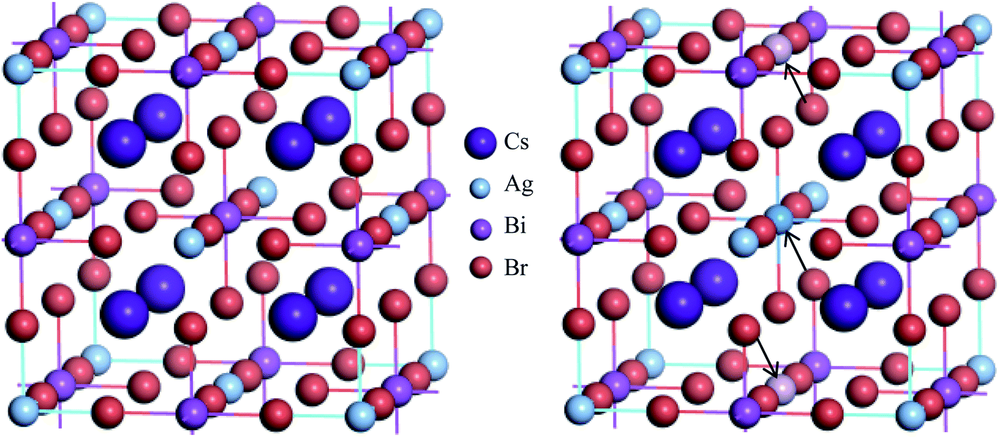 | ||
| Fig. 1 Unit cell of Cs2AgBiBr6; (left) ordered conventional cell, (right) disordered supercell (1 × 1 × 1). In supercell, the body centered Bi atom is substituted by Ag atom (deep colored) and two Ag atoms from upper and lower faces are replaced by two Bi atoms (light colored). | ||
To change into direct band gap disordered Cs2AgBiBr6 material, a body centered Bi atom from the ordered supercell of Cs2AgBiBr6 is replaced by an Ag atom and two face centered Ag atoms are substituted with two Bi atoms since one face centered atom contribute half to the cell (see Fig. 1). As a result, the lattice parameter of disordered system reduces slightly due to ionic mismatch of Bi3+ (1.03 Å) and Ag1+ (1.15 Å).
A complete study of the stability of the disordered compound Cs2AgBiBr6 will require the calculation of both the dynamical (phonon dispersion relations) and thermodynamic (quaternary convex hulls) stability. Since these calculations require high computational resources and are time consuming, we make initial assessment of compound stability through calculating the final energy, decomposition enthalpy and tolerance and octahedral factors. We obtained that the final energy of −448.30 eV per atom for disordered Cs2AgBiBr6 is comparable to −448.32 eV per atom of its corresponding ordered system. This implies that the disordered Cs2AgBiBr6 is as stable compound as it ordered system.
To assess thermodynamic stability of Cs2AgBiBr6 perovskite, we calculate its decomposition energy with respect to possible pathways. The modest and predominant one is the decomposition of Cs2AgBiBr6 into corresponding binary materials. Halide perovskites are usually synthesized via their inverse reactions. Specifically, we calculate the decomposition enthalpy defined as:
| ΔH = 2E[CsBr] + E[AgBr] + E[BiBr3] – E[Cs2AgBiBr6] |
According to Goldschmidt's empirical criteria,41 the tolerance factor t and the octahedral factor μ for a perovskite with formula ABX3 can be defined as t = (RA + RX)/√2(RB + RX) and μ = RB/RX, with RA, RB, and RX being the ionic radii of the elements in a ABX3 perovskite. The stable structures require to have 0.75 < t < 1.0 and μ > 0.41.42 To evaluate these parameters, we use Shannon ionic radii. Since we have double perovskite and therefore different radii for B+ and B3+ sites, we consider the average between the radii of Ag+ and Bi3+ for RB. The Shannon ionic radii of Cs, Ag, Bi and Br are 1.67, 1.15, 1.03, and 1.96 Å, respectively. Therefore, the tolerance and octahedral factors for Cs2AgBiBr6 are 0.84 and 0.56, respectively. These values are applicable for both the ordered and disordered Cs2AgBiBr6 double perovskites as the disordered system contains the same atoms as the ordered system has. Thus the disordered system is as stable as the ordered system is.
3.2. Electronic structures
To understand the electronic structures of ordered and disordered cubic lead free metal halide double perovskite Cs2AgBiBr6, we have investigated the electronic band structures along the high symmetry directions. The band structures of ordered and disordered systems are shown in Fig. 2. In the ordered compound, the valence band maximum (VBM) appears at the Γ-point on the Fermi level while the conduction band minimum (CBM) appears on the L above the Fermi level. Therefore, the ordered Cs2AgBiBr6 is an indirect band gap material. The band gap of ordered Cs2AgBiBr6 is 2.04.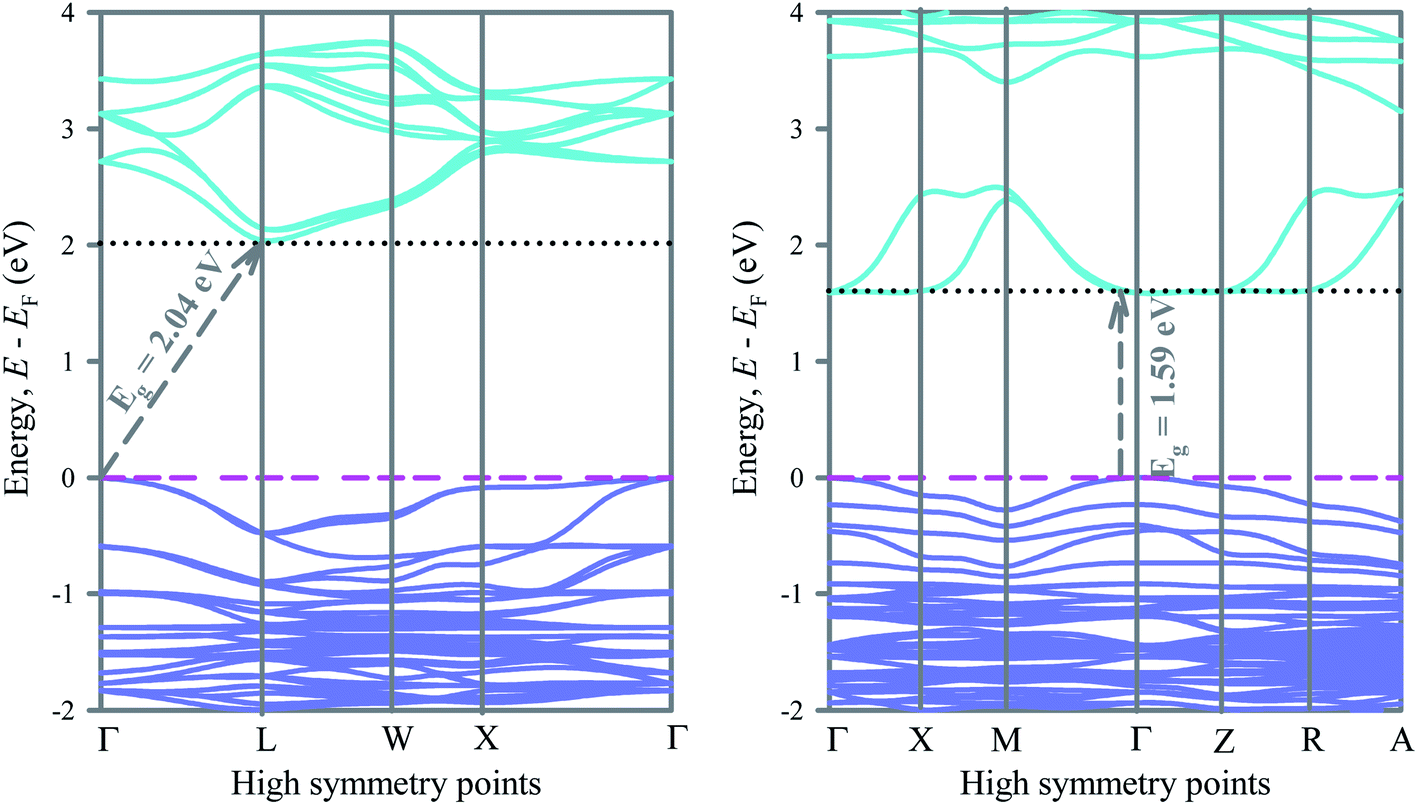 | ||
| Fig. 2 Electronic band structure of ordered (left) and disordered (right) of Cs2AgBiBr6. | ||
In the disordered Cs2AgBiBr6, the Bi 6p orbital modifies the conduction band significantly and leads to shift the CBM from L to Γ-point. Consequently, the system changes from indirect to direct band gap material. At the same time the band gap reduces significantly. The band gap of Cs2AgBiBr6 decreases from 2.04 eV to 1.59 eV when the system changes from order to disorder. Switching from order to disorder system leads to modify the band structures of Cs2AgBiBr6 and converts it from indirect to direct band gap material. A previous study17 reported the band gap of ordered Cs2AgBiBr6 with the hybrid functional HSE06 is 2.06 eV, which is very close to the present value obtained with the same functional.
In particular, the conduction band due to the Bi 6d orbital has changed significantly after the system switched from order to disorder system. Lower conduction bands change their shape from convex to concave along the Γ-point and keep the CBM at the Γ-point above the Fermi level and reduce the band gap and change the nature (indirect to direct) of bandgap. However, as the system changes from order to disorder, the lower conduction band along the W–X direction changes from convex to plane. Direct band gap materials are promising for photovoltaic and optoelectronic applications. Generally, a direct bandgap semiconductor has a less effective mass of electrons than an indirect bandgap semiconductor of the same bandgap. This means that electrons travel more rapidly in a direct band gap semiconductor than in an indirect bandgap semiconductor. It can be seen that the conduction band of the disordered Cs2AgBiBr6 is aligned just above the valence band, which gives rise to energy emission in the form of light during recombination. So, the disordered Cs2AgBiBr6 is appropriate for photovoltaic devices such as solar cells, lasers, LEDs, photoconductors, phototransistors, etc. The disordered Cs2AgBiBr6 has suitable direct band gap of 1.59 eV. The fairly suitable band gap endows the disordered double perovskite with the proficiency to absorb solar energy in the wide range of spectrum.
Fig. 3 depicts the total and partial density of states of ordered and disordered Cs2AgBiBr6 double perovskites that make clear the contribution in the band structures from the individual atoms. In both ordered and disordered Cs2AgBiBr6, the main contributions to the upper valence band below the Fermi level (0 to ∼−1.4 eV) come from Ag 4d and Br 4p orbitals. In ordered Cs2AgBiBr6, some contributions also come from Cs 5p and Bi 6p electrons while in disordered Cs2AgBiBr6, no contribution comes from Cs and a negligible contribution comes from Bi 6p electrons. The middle valence bands (∼−1.4 to −4.3 eV) of both ordered and disordered Cs2AgBiBr6 arise due to strong hybridization between Ag 4d and Br 4p states. The lowest valence bands (−4.3 to −5.2 eV) of both ordered and disordered Cs2AgBiBr6 originate from the strong contribution of Bi 6p and Br 4p states. The entire conduction bands of both ordered and disordered Cs2AgBiBr6 are dominated by Bi 6p states. Indeed, the modification of conduction band due to Bi 6p states via transforming the Cs2AgBiBr6 from order to disorder system leads to the transition of system from indirect to direct bandgap material. The Bi 6p states exist at the bottom of conduction band edge while the Ag 4d states appear at the Fermi level. The possible transitions may be resulted from Ag 4d to Bi 6p states. Therefore, the p–d hybridizations may be responsible for excitation and recombination rate.
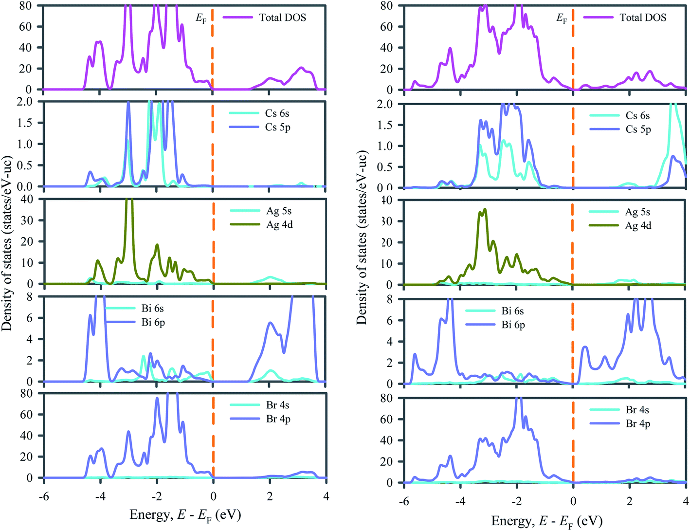 | ||
| Fig. 3 Electronic density of states of ordered (left) and disordered (right) Cs2AgBiBr6. | ||
The bond length of the Ag–Br bond in the order Cs2AgBiBr6 is 2.85405 Å, which decreases to 2.79871 Å when Cs2AgBiBr6 is converted into a disorder system. Again, the bond length of Bi–Br in Cs2AgBiBr6 reduces from 2.86109 Å to 2.81776 Å, when the system is converted into disorder from order system. The contraction of the bond length in the disorder system can cause the bandgap to decrease and the nature of the bandgap to change from indirect to direct.
To visualize the charge distribution and bonding nature of ordered and disordered Cs2AgBiBr6 double perovskites the charge density map is investigated and presented in Fig. 4. Fig. 4 shows that the charge distribution and bonding nature are identical in both (100) and (001) planes. Ag atom is bonded covalently with Br and Bi atom is also bonded covalently with Br in both ordered and disordered Cs2AgBiBr6. Electron clouds around Ag/Bi and Br atoms are distorted towards each other and overlapped considerably, indicating the covalent nature of bonding. The electron clouds around Cs atoms in the (110) planes are spherical without any distortion, indicating its ionic bonding with surrounding atoms. Changing Cs2AgBiBr6 to a disorder system does not change the nature of the bonding but only changes the bond length and bond population.
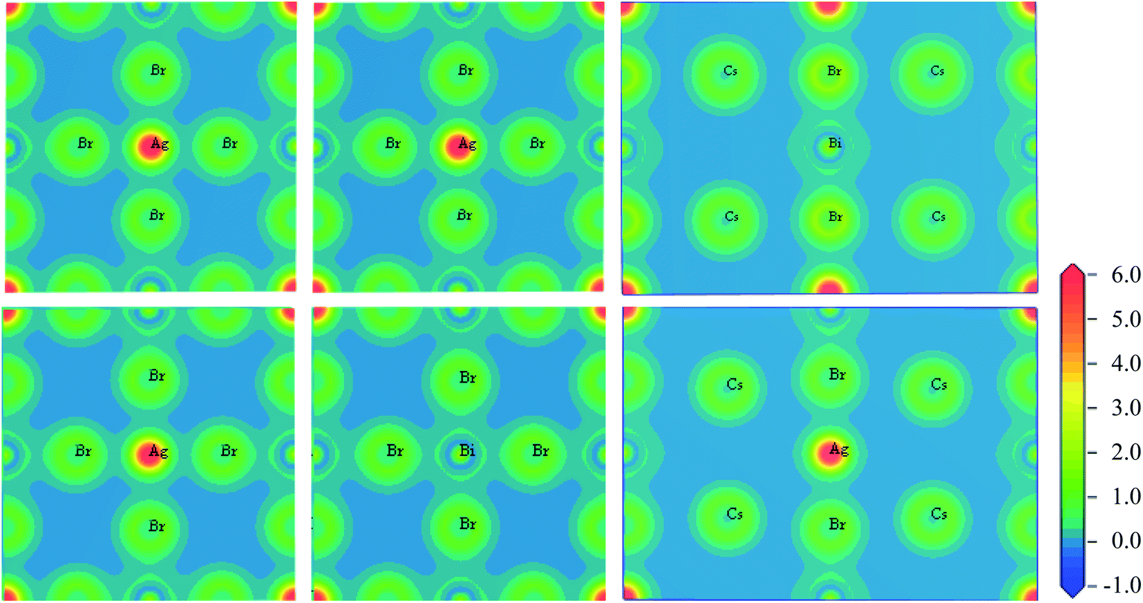 | ||
| Fig. 4 Charge density map of Cs2AgBiBr6 in the planes (100), (001), and (110) from left to right. The upper panels for ordered system and the lower panels for disordered system. | ||
3.3. Optical properties
To study the optical properties of semiconductors is important as their applications in different fields depend on the optical absorption, dielectric function, reflectivity, etc. The optical properties of ordered and disordered Cs2AgBiBr6 double perovskites are calculated using the same code and hybrid functional HSE06. This code is embedded with the formalism used to calculate the optical properties of semiconductors. The imaginary part of dielectric function leads to calculate the other optical functions. The expression used to calculate the imaginary part of dielectric function is as follows:43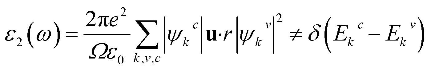
In this expression, the symbols ω, e, Ω, and u successively refer to the phonon frequency, electronic charge, unit cell volume, and unit vector along the polarization of the incident electric field. The symbols ψkc and ψkv define the wave functions for conduction and valence band electrons at a certain k, respectively. The delta function δ approves the conservation of energy and momentum during a transition between the occupied and the unoccupied electronic states through the emission or absorption of a photon with energy E. Finally, Ekc and Ekv denote the energy of electrons at a specific k-vector in the conduction and valence bands, respectively. The rest of optical functions were calculated using the expressions described in a recent paper.44
The absorption process of electromagnetic wave such as light is characterized by the absorption coefficient α(ω), which is typically expressed in unit of cm−1. It depends on the incident photon energy and determines the ratio of the number of photons truly absorbed by the crystal per unit volume per second to the number of incident photons per unit area per second. It is observed that the absorption occurs at low energy regions in disordered systems compared to their ordered ones (refer to Fig. 5a). On the other hand, the declination of absorption spectra occurs at slightly higher energy regions for disordered systems. It means that the absorption takes place in a wide range of photon energies. This range covers the full visible and ultraviolet solar spectra. The absorption edge towards the lower energy region and strong optical absorption in the visible to UV region points out that the disordered systems are appropriate for use in solar cells and optoelectronic and energy harvesting devices.
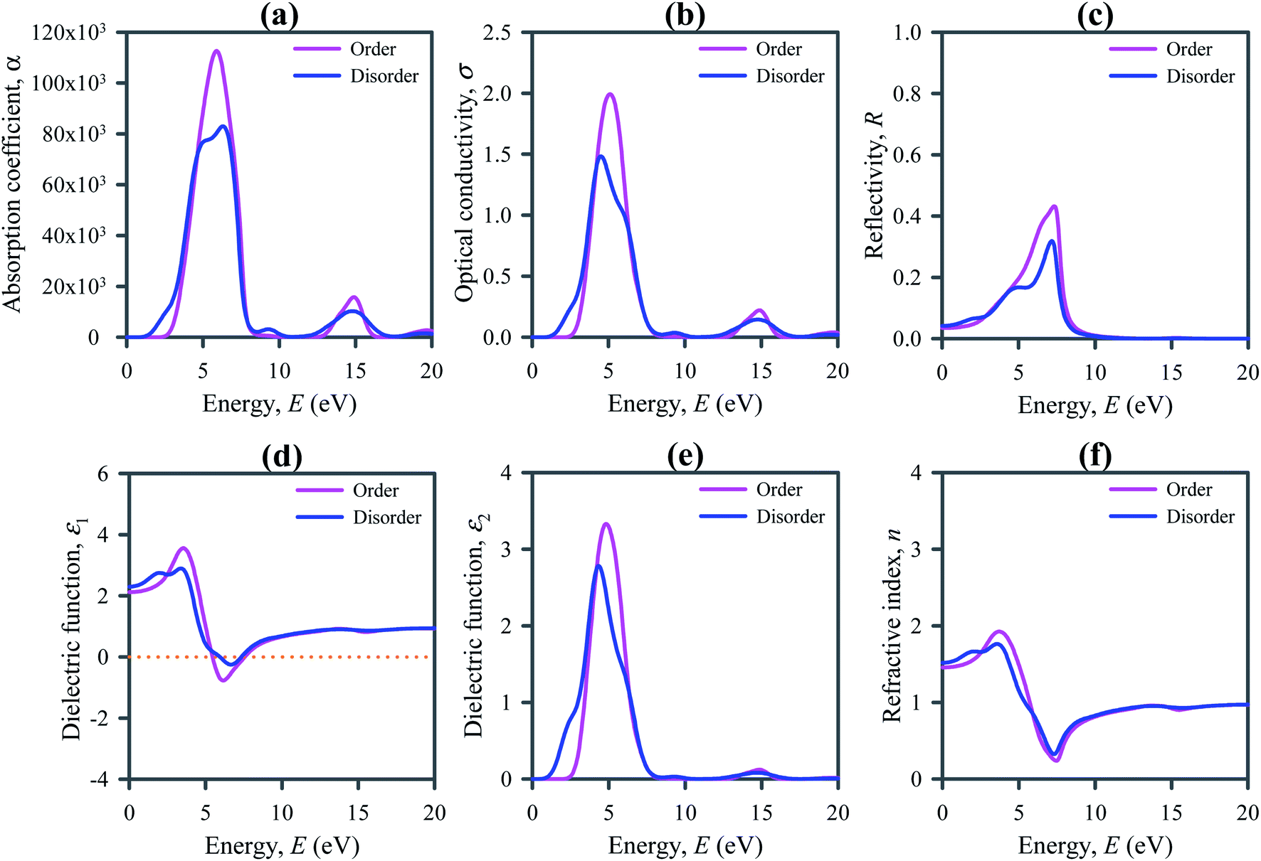 | ||
| Fig. 5 Optical properties of ordered and disordered Cs2AgBiBr6; (a) absorption coefficient (in cm−1), (b) optical conductivity, (c) reflectivity, (d) real part of dielectric function, (e) imaginary part of dielectric function, and (f) refractive index. | ||
Optical conductivity is the extension of electrical transport at high optical frequencies. It is a contact-free quantitative measure, sensitive to most charged responses. The study of optical conductivity σ(ω) is significant for the selection of materials used in optoelectronic devices. The calculated optical conductivity is presented in Fig. 5b. The optical conductivity of the disordered Cs2AgBiBr6 occurs at lower energies than its ordered system, indicating the absorption of light at lower photon energy. The optical conductivity increases rapidly with the increase of photon energy and reaches a maximum value at about 5 eV as optical absorption does. Low energy optical conductivity makes disordered Cs2AgBiBr6 a potential candidate material for applications in solar cells and optoelectronic devices.
Reflectivity is an additional optical factor that serves as a useful indicator for optoelectronic uses of semiconductors. Low reflectivity is always related to the high absorption of light. Fig. 5c depicts the reflectivity calculated for Cs2AgBiBr6, showing a low reflectivity in the entire IR and visible light regions in addition to the low-energy part of the UV region of the solar spectra. The low reflectivity of Cs2AgBiBr6 indicates that it has high absorptivity of light. In the visible and low-energy part of the UV regions the reflectivity of disordered system is slightly small compared to the ordered systems.
Dielectric function assesses the response to electromagnetic radiation of a substance. It is an important property of a semiconductor for its optoelectronic applications because the high dielectric constant refers to weak Coulomb interaction and is linked to the low charge carrier reconnection rate and the overall performance of an optoelectronic device. Fig. 5d depicts the real part of dielectric function ε1(ω) calculated for ordered and disordered Cs2AgBiBr6 double perovskites. The static value of ε1 is slightly larger for disordered Cs2AgBiBr6 compared to the ordered system.
The imaginary part of the dielectric function ε2(ω) signifies the optical absorption of a material and is linked to the real part of the optical conductivity. Fig. 5e shows the calculated ε2(ω) for Cs2AgBiBr6, signifying the good absorption of light in the visible and UV regions. The spectrum range for absorption is slightly wider for disordered Cs2AgBiBr6 compared to the ordered system. It means that the disordered Cs2AgBiBr6 is a good absorber in this region.
The knowledge of refractive index n(ω) of a semiconductor is important for its use in optoelectronic devices such as solar cells, optical waveguides, light emitting diode (LED), photonic crystals, and detectors. Fig. 5f presents the calculated refractive index n(ω) of Cs2AgBiBr6. The static refractive index of disordered Cs2AgBiBr6 is slightly higher than that of their ordered system. Direct bandgap semiconductors with high refractive index are extremely useful for optoelectronic applications, for example, LCD displays, waveguides, etc.
3.4. Mechanical properties
The investigation of elastic constants of materials is important as they can provide the information about the bonding nature and mechanical properties of crystalline solids. The cubic crystals like investigated double perovskite have three independent elastic constants such as C11, C12, and C44. Table 2 lists the calculated values of elastic constants for Cs2AgBiBr6. To be mechanically stable the elastic constants of a cubic crystal must satisfy the born stability conditions:45| C44 > 0, C11−C12 > 0 and C11 + 2C12 > 0 |
| System | Cell | C11 | C12 | C44 | C11−C44 | B | G | B/G | v |
|---|---|---|---|---|---|---|---|---|---|
| Order | Unit cell | 38.76 | 9.19 | 7.58 | 31.18 | 17.89 | 10.18 | 1.76 | 0.261 |
| Disorder | Supercell | 48.84 | 13.55 | 7.37 | 41.47 | 24.84 | 10.22 | 2.43 | 0.319 |
The listed values of elastic constants in Table 2 satisfy the above conditions and thus ensure the mechanical stability of both ordered and disordered Cs2AgBiBr6 double perovskites. All crystalline solids are characterized by a failure mode (either brittleness or ductility), which controls the applications of solid materials. Cauchy pressure, defined as C11–C44, can classify the solid materials into two groups: brittle and ductile. A ductile material has positive Cauchy pressure while a brittle material possesses a negative Cauchy pressure.46 Both the ordered and disordered double perovskites studied here characterized with positive Cauchy pressure and consequently they are ductile in nature. Changing Cs2AgBiBr6 to disorder system improves its ductility. The ductility is an essential property of a semiconductor for being used in optoelectronic and photovoltaic applications. In fabrication into thin film a semiconductor must be ductile in nature.
The bulk modulus B is calculated to be 17.89 (24.84) GPa for ordered (disordered) Cs2AgBiBr6 double perovskite. The calculated shear modulus G is 10.18 (10.22) GPa for ordered (disordered) Cs2AgBiBr6. These values are small enough for the double perovskite studied here to be flexible and soft.47 As a result, the double perovskite under study can easily be fabricated into a thin film and make them more effective in photovoltaic applications such as solar cells. The Pugh's ratio, B/G and Poisson's ratio, v = (3B – 2G)/(6B + 2G) can be used to predict the brittle/ductile nature in solids. The threshold value of 1.75 (0.26) for Pugh' ratio (Poisson's ratio) is used as the border line between ductility and brittleness of compounds.48,49 In addition to the high value of Pugh's ratio of 1.75, the high value of Poisson's ratio of 0.26 is related to the ductile materials and low values are linked to the brittle materials. Both these scales indicate the ductile nature of both order and disorder double perovskites studied here. This prediction is a cross-check of above prediction from Cauchy pressure. We have previously mentioned that the ductile nature of semiconductors makes them suitable for use in optoelectronic and photovoltaic devices.
4. Conclusions
In summary, the structural, electronic, optical and mechanical properties of lead-free non-toxic inorganic metallic halide cubic double perovskite Cs2AgBiBr6 is investigated in its order and disorder forms using DFT to authenticate their photovoltaic and optoelectronic applications. The indirect bandgap of Cs2AgBiBr6 is tuned to direct bandgap by changing them from order to disorder system following the disordering of Ag+/Bi3+ cations by creating an antisite defect in the sublattice. In the disordered Cs2AgBiBr6, the Bi 6p orbital modifies the conduction band significantly and leads to tune the band gap from indirect to direct. The band gap of Cs2AgBiBr6 decreases from 2.04 eV to 1.59 eV. The reduction in band gap allows the disorder system to absorb the light from visible spectrum. The absorption edge towards the lower energy region and strong optical absorption in the visible to UV region signifies that the disordered direct band gap material Cs2AgBiBr6 is suitable for use in solar cells and optoelectronic and energy harvesting devices. Other optical functions including dielectric function, reflectivity and refractive index of disorder Cs2AgBiBr6 is auspicious for its optoelectronic and photovoltaic applications. The stability and ductility of disordered Cs2AgBiBr6 is also favorable in its thin film fabrication. Hopefully, this study will encourage the experimental synthesis of disordered Cs2AgBiBr6 by creating antisite defects in the sub-lattice. However, this study will open a new avenue for designing high-performing optoelectronic and photovoltaic materials.Author contributions
M. A. Hadi: Conceptualization, Investigation, Methodology, Data curation, Formal analysis, Writing-original draft. M. N. Islam: Investigation, Validation. J. Podder: Validation, Visualization.Conflicts of interest
There are no conflicts to declare.Acknowledgements
The authors wish to acknowledge the computational facility to calculate the elastic properties for the considered double perovskite at the Department of Physics, Bangladesh University of Engineering and Technology, Dhaka, Bangladesh.References
- H. Zhou, Q. Chen, G. Li, S. Luo, T. B. Song, H. S. Duan, Z. Hong, J. You and Y. Yang, Interface engineering of highly efficient perovskite solar cell, Science, 2014, 345, 542–546 CrossRef CAS PubMed.
- J. Burschka, N. Pellet, S.-J. Moon, R. Humphry-Baker, P. Gao, M. K. Nazeeruddin and M. Grätzel, Sequential deposition as a route to high-performance perovskite-sensitized solar cells, Nature, 2013, 499, 316–319 CrossRef CAS PubMed.
- A. B. Wong, M. Lai, S. W. Eaton, Y. Yu, E. Lin, L. Dou, A. Fu and P. Yang, Growth and anion exchange conversion of CH3NH3PbX3 nanorod arrays for light-emitting diodes, Nano Lett., 2015, 15, 5519–5524 CrossRef CAS PubMed.
- Y. Fu, H. Zhu, A. W. Schrader, D. Liang, Q. Ding, P. Joshi, L. Hwang, X.-Y. Zhu and S. Jin, Nanowire lasers of formamidinium lead halide perovskites and their stabilized alloys with improved stability, Nano Lett., 2016, 16, 1000 CrossRef CAS PubMed.
- E. Zheng, B. Yuh, G. A. Tosado and Q. Yu, Solution processed visible-blind UV-A photo detectors based on CH3NH3PbCl3 perovskite thin films, J. Mater. Chem. C, 2017, 5, 3796 RSC.
- E. T. Hoke, D. J. Slotcavage, E. R. Dohner, A. R. Bowring, H. I. Karunadasa and M. D. McGehee, Reversible photo-induced trap formation in mixed-halide hybrid perovskites for photovoltaics, Chem. Sci., 2015, 6, 613–617 RSC.
- C. Eames, J. M. Frost, P. R. F. Barnes, B. C. O'Regan, A. Walsh and M. Saiful Islam, Ionic transport in hybrid lead iodide perovskite solar cells, Nat. Commun., 2015, 6, 7497 CrossRef CAS PubMed.
- J. S. Manser, M. I. Saidaminov, J. A. Christians, O. M. Bakr and P. V. Kamat, Making and Breaking of Lead-Halide Perovskites, Acc. Chem. Res., 2016, 49, 330–338 CrossRef CAS PubMed.
- F. Giustino and H. J. Snaith, Toward Lead-Free Perovskite Solar Cells, ACS Energy Lett., 2016, 1, 1233 CrossRef CAS.
- C. C. Stoumpos, L. Frazer, D. J. Clark, Y. S. Kim, S. H. Rhim, A. Freeman, J. B. Ketterson, J. I. Jang and M. G. Kanatzidis, Hybrid germanium iodide perovskite semiconductors: active lone pairs, structural distortions, direct and indirect energy gaps, and strong nonlinear optical properties, J. Am. Chem. Soc., 2015, 137, 6804 CrossRef CAS PubMed.
- J. Zhou, Z. Xia, M. S. Molokeev, X. Zhang, D. Peng and Q. Liu, Composition design, optical gap and stability investigations of lead free halide double perovskite Cs2AgInCl6, J. Mater. Chem. A, 2017, 5, 15031–15037 RSC.
- A. Abate, Perovskite Solar Cells Go Lead Free, Joule, 2017, 1, 887 CrossRef.
- X. G. Zhao, J. H. Yang, Y. H. Fu, D. W. Yang, Q. L. Xu, L. P. Yu, S. H. Wei and L. J. Zhang, Design of Lead-Free Inorganic Halide Perovskites for Solar Cells via Cation-Transmutation, J. Am. Chem. Soc., 2017, 139, 2630 CrossRef CAS PubMed.
- M. Lyu, J.-H. Yun, P. Chen, M. Hao and L. Wang, Addressing Toxicity of Lead: Progress and Applications of Low-Toxic Metal Halide Perovskites and Their Derivatives, Adv. Energy Mater., 2017, 7, 1602512 CrossRef.
- I. N. Flerov, M. V. Gorev, K. S. Aleksandrov, A. Tressaud, J. Grannec and M. Couzi, Phase transitions in elpasolites (ordered perovskites), Mater. Sci. Eng., R, 1998, 24, 81 CrossRef.
- G. Volonakis, M. R. Filip, A. A. Haghighirad, N. Sakai, B. Wenger, H. J. Snaith and F. Giustino, Lead-Free Halide Double Perovskites via Heterovalent Substitution of Noble Metals, J. Phys. Chem. Lett., 2016, 7, 1254 CrossRef CAS PubMed.
- E. T. McClure, M. R. Ball, W. Windl and P. M. Woodward, Cs2AgBiX6 (X = Br, Cl): new visible light absorbing, lead-free halide perovskite semiconductors, Chem. Mater., 2016, 28, 1348–1354 CrossRef CAS.
- M. R. Filip, S. Hillman, A. A. Haghighirad, H. J. Snaith and F. Giustino, Band Gaps of the Lead-Free Halide Double Perovskites Cs2BiAgCl6 and Cs2BiAgBr6 from Theory and Experiment, J. Phys. Chem. Lett., 2016, 7, 2579–2585 CrossRef CAS PubMed.
- P. Zhang, J. Yang and S.-H. Wei, Manipulation of Cation Combination and Configuration of Halide Double Perovskites for Solar Cell Absorbers, J. Mater. Chem. A, 2018, 6, 1 Search PubMed.
- A. H. Slavney, T. Hu, A. M. Lindenberg and H. I. Karunadasa, A Bismuth-Halide Double Perovskite with Long Carrier Recombination Lifetime for Photovoltaic Applications, J. Am. Chem. Soc., 2016, 138, 2138–2141 CrossRef CAS PubMed.
- Z. Xiao, K. Z. Du, W. Meng, J. Wang, D. B. Mitzi and Y. Yan, Intrinsic Instability of Cs2In(I)M(III)X6 (M = Bi, Sb; X = Halogen) Double Perovskites: A Combined Density Functional Theory and Experimental Study, J. Am. Chem. Soc., 2017, 139, 6054–6057 CrossRef CAS PubMed.
- X. Ma, Z. Li and J. Yang, J. Phys. Chem. C, 2021, 125, 10868–10875 CrossRef CAS.
- Y. Jiao, S. Zhang, Z. Yang and G. Lu, Comput. Theor. Chem., 2019, 1148, 55–59 CrossRef CAS.
- P. Hohenberg and W. Kohn, Phys. Rev., 1964, 136, B864 CrossRef.
- W. Kohn and L. J. Sham, Phys. Rev., 1965, 140, A1133 CrossRef.
- S. J. Clark, M. D. Segall, C. J. Pickard, P. J. Hasnip, M. I. J. Probert, K. Refson and M. C. Payne, Z. Kristallogr., 2005, 220, 567 CAS.
- D. C. Langreth and M. J. Mehl, Phys. Rev. B: Condens. Matter Mater. Phys., 1983, 28, 1809 CrossRef CAS.
- A. D. Becke, Phys. Rev. A, 1988, 38, 3098 CrossRef CAS PubMed.
- J. P. Perdew, K. Burke and M. Ernzerhof, Phys. Rev. Lett., 1996, 77, 3865 CrossRef CAS PubMed.
- H. J. Monkhorst and J. D. Pack, Phys. Rev. B: Solid State, 1976, 13, 5188 CrossRef.
- D. Vanderbilt, Phys. Rev. B: Condens. Matter Mater. Phys., 1990, 41, 7892 CrossRef PubMed.
- T. H. Fischer and J. Almlof, J. Phys. Chem., 1992, 96, 9768 CrossRef CAS.
- F. D. Murnaghan, Finite Deformation of an Elastic Solid, Wiley, New York, 1951 Search PubMed.
- W. Yuan, G. Niu, Y. Xian, H. Wu, H. Wang, H. Yin, P. Liu, W. Li and J. Fan, Adv. Funct. Mater., 2019, 29, 1900234 CrossRef.
- T. T. Tran, J. R. Panella, J. R. Chamorro, J. R. Morey and T. M. McQueen, Mater. Horiz., 2017, 4, 688–693 RSC.
- A. H. Slavney, T. Hu, A. M. Lindenberg and H. I. Karunadasa, J. Am. Chem. Soc., 2016, 138, 2138–2141 CrossRef CAS PubMed.
- L. Schade, A. D. Wright, R. D. Johnson, M. Dollmann, B. Wenger, P. K. Nayak, D. Prabhakaran, L. M. Herz, R. Nicholas, H. J. Snaith and P. G. Radaelli, ACS Energy Lett., 2019, 4, 299–305 CrossRef CAS.
- J. Yang, P. Zhang and S.-H. Wei, J. Phys. Chem. Lett., 2018, 9, 31–35 CrossRef CAS PubMed.
- L. Dong, S. Sun, Z. Deng, W. Li, F. Wei, Y. Qi, Y. Li, X. Li, P. Lu and U. Ramamurty, Comput. Mater. Sci., 2018, 141, 49–58 CrossRef CAS.
- M. A. Ghebouli, T. Chihi, B. Ghebouli and M. Fatmi, Chin. J. Phys., 2018, 56, 323–330 CrossRef CAS.
- V. M. Goldschmidt, Ber. Dtsch. Chem. Ges., 1927, 60, 1263–1268 CrossRef.
- C. Li, X. Lu, W. Ding, L. Feng, Y. Gao and Z. Guo, Acta Crystallogr., Sect. B: Struct. Sci., 2008, 64, 702–707 CrossRef CAS PubMed.
- M. A. Hadi, Md Roknuzzaman, M. T. Nasir, U. Monira, S. H. Naqib, A. Chroneos, A. K. M. A. Islam, J. A. Alarco and K. Ostrikov, Sci. Rep., 2021, 11, 3410 CrossRef CAS PubMed.
- M. A. Hadi, R. V. Vovk and A. Chroneos, J. Mater. Sci.: Mater. Electron., 2017, 27, 11925 CrossRef.
- M. Born, Math. Proc. Camb. Philos. Soc., 1940, 36, 160 CrossRef CAS.
- M. H. K. Rubel, M. A. Hadi, M. M. Rahaman, M. S. Ali, M. Aftabuzzaman, R. Parvin, A. K. M. A. Islam and N. Kumada, Comput. Mater. Sci., 2017, 138, 160–165 CrossRef CAS.
- M. N. Islam, M. A. Hadi and J. Podder, AIP Adv., 2019, 9, 125321 CrossRef.
- M. A. Hadi, Comput. Mater. Sci., 2016, 117, 422–427 CrossRef CAS.
- M. A. Hadi, J. Phys. Chem. Solids, 2020, 138, 109275 CrossRef CAS.
Footnote |
| † Dedicated to: Emeritus Professor Dr Arun Kumar Basak on the occasion of his 80th birthday. |
| This journal is © The Royal Society of Chemistry 2022 |