
Copper-incorporation for polytypism and bandgap engineering of MAPbBr3 perovskite thin films with enhanced near-Infrared photocurrent-response†
Amr
Elattar
 *ab,
Jiban
Kangsabanik
c,
Kodai
Nakao
a,
Kosei
Tsutsumi
a,
Hiroo
Suzuki
a,
Takeshi
Nishikawa
a,
Kristian S.
Thygesen
c and
Yasuhiko
Hayashi
a
*ab,
Jiban
Kangsabanik
c,
Kodai
Nakao
a,
Kosei
Tsutsumi
a,
Hiroo
Suzuki
a,
Takeshi
Nishikawa
a,
Kristian S.
Thygesen
c and
Yasuhiko
Hayashi
a
aGraduate School of Natural Science and Technology, Okayama University, 3-1-1 Tsushimanaka, Kita-ku, Okayama 700-8530, Japan. E-mail: psgx8nrx@s.okayama-u.ac.jp
bDepartment of Chemistry, Faculty of Science, Ain Shams University, 11566 Cairo, Egypt
cCAMD, Department of Physics, Technical University of Denmark, 2800 Kongens Lyngby, Denmark
First published on 2nd August 2022
Abstract
The optoelectronic properties of lead-based halide perovskites can be enhanced through B-site engineering. Here, we studied the B-site alloying of MAPbBr3 thin films with copper (Cu2+). The alloyed perovskite thin films were characterized by a dark color, enlarged average grain boundary, and lowering of the optical bandgap from 2.32 eV for pristine MAPbBr3 to 1.85 eV for 50% Cu-substituted MAPbBr3. Various characterization methods revealed that the Cu-incorporation leads to the appearance of a Cu-rich secondary phase. The conductivity increased over three orders of magnitude upon alloying. Temperature-dependent conductivity measurements at temperatures ranging from 110 K to 300 K revealed the occurrence of two phase-transitions in Cu-substituted perovskite, and only one transition in pristine MAPbBr3. Photocurrent measurements of the alloyed perovskites showed that band-carrier generation occurred upon excitation in the near-infrared region. First-principles point defect calculation shows the likelihood of compensating Br vacancy formation with high Cu-substituting concentrations. Calculation of atomic orbital projected density of states (CuPb + vBr defect complex) revealed the presence of localized defect states within the pristine bandgap, explaining the observed sub-bandgap absorption. The results provide an insight into the alloying importance in phase-modulation and tailoring the optoelectronic properties of perovskites for a wide range of efficient optoelectronic devices.
Introduction
Lead-based perovskites have been widely utilized in optoelectronic devices, owing to their attractive features of strong absorption coefficient,1–3 high charge carrier mobility,4–8 tunable bandgap,9–12 long diffusion length,13–15 and low exciton binding energies.16–19 One of the fundamental approaches to developing efficient perovskite-based optoelectronic devices is doping/alloying. Via doping, defect/impurity levels, introduced by dopants, overlap with the valence band (or the conduction band) of the host perovskite. As a result, different perovskites with versatile optical and electrical properties can be manipulated. Three types of MAPbX3 doping have (in general) been investigated in numerous studies: (1) A-site doping where a methylammonium MA+ cation is doped with A+ (A+ = FA+, Rb+, Cs+, or K+).20–30 (2) B-site doping where lead Pb2+ is doped with different metal cations Mn+ (Mn+ = Sn2+, Ca2+, Cd2+, Sr2+, Bi3+, Au3+, Ba2+, Mn2+, Ni2+, In3+, Cu2+, or Er3+).31–44 (3) Halide anion X− doping with different anions (Cl−, Br−, I−, or Se2−).45–49MAPbBr3 perovskite has considerable potential for laser applications50–53 and photodetection.54,55 Various investigations have focused on enhancing the optoelectronic properties of this material via doping. Deng et al. have studied NH4+-doped MAPbBr3 perovskite quantum dots.56 They found that NH4+ inhibits non-radiative recombinations and reduces the defect density of MAPbBr3. Li et al. have proposed local lattice strain compensation of Zn2+-doped MAPbBr3 single crystal for photo-restriction under light illumination.57 Furthermore, through Er3+-doping, the responsivity and external quantum efficiency of MAPbBr3 single crystal photodetector increased five-fold relative to that of the pristine crystal.44 Moreover, Bi3+-doped MAPbBr3 single crystals have been extensively investigated. Early investigations by Abdelhady et al. suggested that Bi-doping-induced changes in the absorption spectrum resulted from bandgap modulation.39 However, subsequent studies showed that Bi-doping increases the trap states within the bandgap of the MAPbBr3 host without any effect on the bandgap and the exciton binding energy.38,40,42,43,58
Polytypism is one example of polymorphism where the crystal structure is identical along two dimensions but different along the third dimension. Polytypism of hybrid lead-based perovskites has been reported in a few papers.59–61 The polytypes of hybrid perovskite structure ABX3 depend on the stacking sequence of the close-packed AX3 layers. The most common polytype of hybrid perovskite is the 3C polytype with BX6 corner-sharing octahedra, which is favorable for perovskites with tolerance factors of t ≤ 1.60 The label of 3C resembles the three close-packed layers of the aristotype cubic cell (C).62 The other most common polytypes of perovskite oxides are hexagonal polytypes, which are favorable for perovskites with tolerance factors of t > 1, which can be obtained through using large A-cations or small B-cations.61 A 2H hexagonal polytype with BX6 face-sharing octahedra leads to a one-dimensional (1D) array.59 However, the other 4H and 6H hexagonal polytypes, which have three-dimensional (3D) frameworks, are composed of BX6 face-sharing octahedra (h) and BX6 corner-sharing octahedra (C).60
In this study, we have investigated the Cu2+-chemical alloying effect on MAPbBr3 as a host material. Upon substitution, MA(Pb:Cu)Br3, thin films exhibit color darkness with increasing size of the average grain boundaries. Optical measurements indicate a sharp bandgap reduction with 50% replacement. X-ray diffraction (XRD), X-ray photoelectron spectroscopy (XPS) and energy dispersive spectroscopy (EDS) mapping measurements indicate that Cu2+ ions are incorporated into the MAPbBr3 crystal structure with the appearance of a new phase related neither to the crystal structure peaks of MAPbBr3 nor the initial precursor. Theoretical simulations were utilized to further explore the Cu-incorporation mechanism. Photocurrent measurements of the doped perovskites revealed band carrier generation at an excitation photon energy below the bandgap, suggesting considerable potential for a wide range of optoelectronic applications.
Results and discussion
Anti-solvent assisted crystallization of methylammonium lead bromide perovskites plays the most significant role in DMF, at the crystallization temperature (70 °C).39 In this work, pristine and Cu-alloyed MACuxPb(1−x)Br3 (where x = 0%, 10%, 20%, 30%, 40%, and 50%) polycrystalline thin films were prepared via spin-coating of the precursor solution over a glass substrate with the assistance of toluene as an anti-solvent, as shown in Fig. 1 The perovskite films with different Cu2+ concentrations differ in color (see Fig. 1b) from yellowish orange for the non-alloyed MAPbBr3 to almost dark brown for the 50% Cu-substituted MAPbBr3.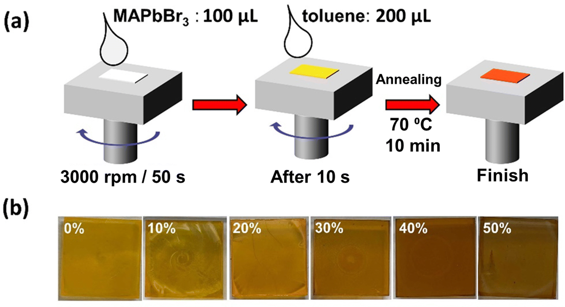 | ||
| Fig. 1 (a) Graphical illustration of perovskite thin film fabrication via spin-coating. (b) Picture of pristine (0%) and (10, 20, 30, 40, and 50%) Cu-substituted MAPbBr3 thin films obtained from use of (0, 10, 20, 30, 40, and 50%) [CuBr2]/([CuBr2] + [PbBr2]) mole percentages. | ||
The top-view scanning electron microscopy (SEM) images presented in Fig. 2a–f show the morphology of the perovskite thin films. Upon Cu2+ alloying, the average grain boundary area increases from 0.042 μm2 for pristine MAPbBr3 to 0.71 μm2 for 40% Cu-substituted MAPbBr3, as shown in Fig. S1 (ESI†). However, an SEM image of the 50% Cu-substituted MAPbBr3 thin film revealed that large micro-rods are formed as a side product. Energy dispersive scanning (EDS) elemental mapping results reveal the presence of homogeneously distributed Pb (blue-colored images in Fig. S2, ESI†). However, the Cu-elemental mapping results (red-colored images in Fig. S2, ESI†) show the gradual increase in Cu alloying. Cu is homogeneously distributed until an alloying level of 20% is reached. After that, a Cu-rich new phase appears in the film which is clearly observed at an alloying level of 50%.
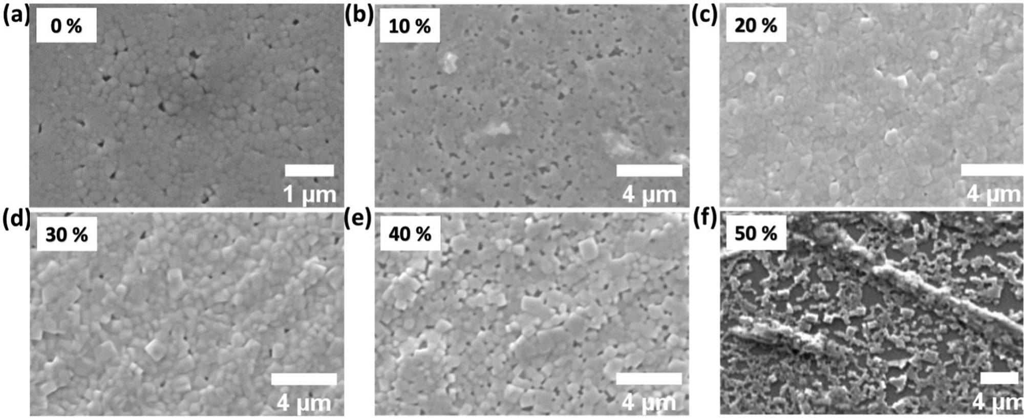 | ||
| Fig. 2 SEM images of undoped (a), 10% (b), 20% (c), 30% (d), 40% (e), and 50% (f) Cu-alloyed MAPbBr3 thin films. | ||
Fig. 3a shows the XRD pattern of the pristine and Cu-substituted MAPbBr3 thin films. The alloyed samples maintain the cubic perovskite structure of MAPbBr3 with three main diffraction peaks at (100), (200), and (300).63 However, with incorporation of Cu into the material, new XRD peaks occur at 2θ = 11.2° (‡) and 2θ = 11.5° (§). Regarding to XRD data within 2theta range 14.6°–15.3° (As depicted in Fig. 3b), the main diffraction peak (100) of MAPbBr3 cubic structure is shifted towards lower theta with increasing of copper alloying from pristine MAPbBr3 into 20% alloyed one. This reveals MAPbBr3 crystal lattice expansion owing to the copper occupation of the interstitial positions through MAPbBr3 cubic structure rather than Cu/Pb metal substitution. This is consistent with the large difference in effective ionic radius of Pb2+ (119 pm) and Cu2+ (73 pm). In addition, Cu perovskites show Jahn–Teller distortion which stereochemically hinders the upkeeping of 3D perovskite structure. With further Cu-alloying, the XRD peak is shifted-back to its original position. This might be accounted for the preference of Cu-atoms to form the Cu-rich secondary phases rather than the occupation of the MAPbBr3 interstitial positions. A plot of the logarithm (intensity) vs. 2θ, as shown in Fig. 3c, reveals four regions. These include the purple regions of 3D-MAPbBr3 and peaks corresponding to crystalline residual metal halide salt in the perovskites with Cu-concentration ranging from 30% to 50% (blue and green regions represent CuBr2 and PbBr2, respectively). Interestingly, the orange region reveals a new diffraction peak, which occurs for 20% Cu-substituted MAPbBr3 (‡). With further substitution, the intensity of this peak decreases while the intensity of another peak (occurring at a higher angle) increases (§). These extra XRD peaks may have resulted from two factors. One factor is that the formation of Pb-substituted 2D Cu-based perovskite secondary phase MA2CuBr4 may have contributed to their emergence. However, this factor can be excluded as the main peak of MA2CuBr4 perovskite should be appeared near 2θ = 9.2° not in the range (11°–12°) whatever the concentration of lead alloyed, as depicted in Fig. S3 (ESI†).64 The other possible factor is the formation of a Pb-based perovskite secondary phase, owing to Cu-alloying. According to literature,60 Pb-based perovskite, namely (FAPbI3)x(MAPbBr3)1−x, exhibits a sequential hexagonal polytypism (i.e., 2H (delta phase)-4H-6H-3R(3C)) during the crystallization process of its perovskite thin film (H, R, and C represent hexagonal, rhombohedral, and cubic phases, respectively). Moreover, the hexagonal phases have one dimensionality (1D) structure with XRD fingerprint peaks for 2θ ranging from 11.6° to 14.1°, and therefore we hypothesize that both peaks, i.e., ‡ and §, correspond to new phases, which are neither related to the crystal structure of 3D-MAPbBr3 nor the initial precursors. These peaks may, however, be related to 1D hexagonal polytypes of Cu-MAPbBr3 perovskite, which would be consistent with the formation of a rod-shaped phase in the 50% Cu-substituted thin film. Regarding to these observations, we speculate that hexagonal polytypes of Cu-substituted MAPbBr3 perovskite. This might be attributed to the presence of MAPbBr3 cubic perovskite which induces the excess copper to form polytypes of the most stable 1D microrods rather than 2D sheets.
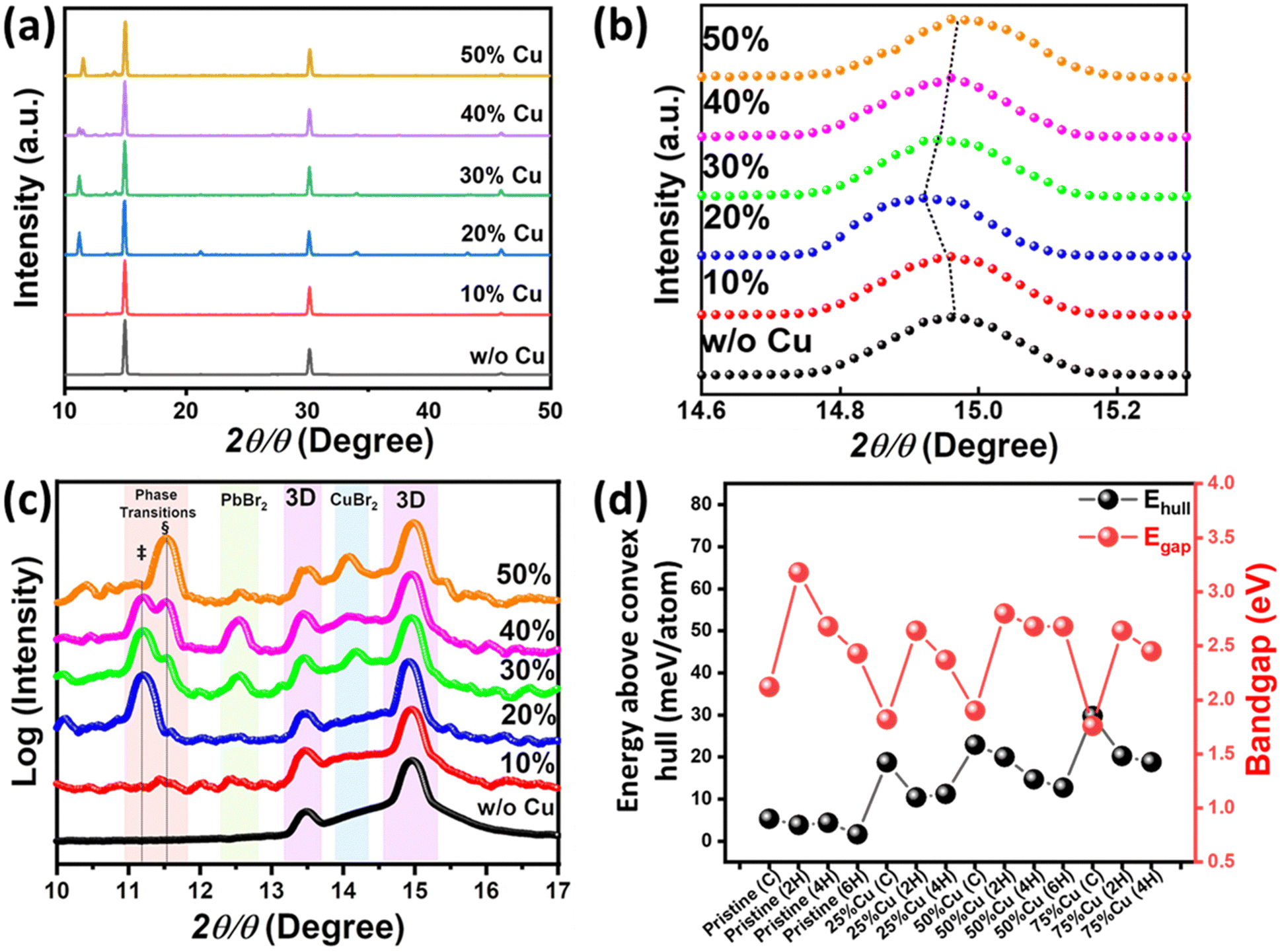 | ||
| Fig. 3 (a) XRD patterns of Cu-alloyed MAPbBr3 perovskite thin films. (b) XRD peak 〈100〉 shift upon copper addition. (c) XRD patterns (log scale) for 2θ = 10–17°. (d) Energy above convex hull and bandgap for different phases of pure and Cu-alloyed MAPbBr3 where C, 2H, 4H, and 6H represent cubic, hexagonal-2H, hexagonal-4H, and hexagonal-6H phases of MAPbBr3, respectively. | ||
To verify the validity of the assumption that hexagonal polytypes are formed in Cu-substituted MAPbBr3, we calculated the energy above the convex hull (Ehull) of different phases (namely Cubic, 2H, 4H, and 6H (only for 50% alloying)) with varying substituted concentrations (MACuxPb1−xBr3; x = 0, 0.25, 0.5, and 0.75). The possible crystal structures are presented in Fig. S4–S7 (ESI†). Fig. 3d shows Ehull calculation results where all possible secondary phases are taken from the Open Quantum Materials Database (OQMD).65Ehull can be seen as a measure of comparative stability between different phases. It should be noted that Ehull is calculated at T = 0 K and a finite temperature might have some effect on comparative stability. For the pristine MAPbBr3 perovskite, almost the same Ehull is obtained for the aforementioned four phases. However, for the Cu-alloyed compounds, the Ehull of the hexagonal phases differs modestly (by ∼10 meV per atom) from that of the cubic phase. This might explain some secondary hexagonal phase formation with Cu alloying as observed experimentally. Furthermore, the bandgap differs among the phases of the Cu-alloyed perovskites with the cubic phase showing the lowest bandgap in all the alloying concentrations. For the hexagonal phase bandgap decreases when we go from 2H > 4H > 6H.
In order to study the effect of Cu2+ incorporation on the elemental composition of Cu-MAPbBr3 films, X-ray photoelectron spectroscopy (XPS) was performed, as depicted in Fig. 4 and Fig. S8 (ESI†). The Pb 4f spectrum for the MAPbBr3 film reveals 4f5/2 and 4f7/2 peaks at 143.4 and 138.6 eV, respectively, corresponding to the Pb2+ cations66 (Fig. 4a). The Br 3d spectrum (Fig. 4b) shows 3d3/2 and 3d5/2 peaks at 69.7 and 68.5 eV, respectively, corresponding to the Br− anions. The C 1s spectrum for the MAPbBr3 film presents C–N and C–C peaks at 286.2 and 284.7 eV, respectively, corresponding to the methylammonium CH3NH3+ cations (Fig. 4c). The non-shifting of Pb 4f, Br 3d, and C 1s peaks, with Cu-alloying, is consistent with the formation of MAPbBr3 film as a major phase. In addition, Cu2+ cations embedded in the film are evident with the presence of Cu 2p3/2 at 932.9 eV67 for 10% and 20% samples which are slightly shifted to lower binding energy at 932.7 eV for higher concentration Cu-alloyed perovskites (Fig. S9a, ESI†), revealing the difference in chemical structure nature of Cu2+ alloyed in perovskite which is consistent with XRD results. The formation of Cu-satellite structure at higher Cu-alloyed samples (Fig. 4d) indicates the presence of Cu2+ species, as expected.68 Gradual increasing of Cu 2p3/2 peak area is a clear indication of increasing of copper concentration embedded in perovskite thin films upon alloying (Fig. S9b, ESI†). Notably, after incorporation of 50% Cu, the Br 3d, and C 1s peaks area is clearly changed which might be attributed to the Cu-rich secondary phase formation. Furthermore, new peaks at 141.4 eV and 136.6 eV are formed through the Pb 4f spectrum which might be assigned to the formation of Pb metal or the Pb occupation of the Cu-rich secondary phase interstitial positions.69 The changes in peak area behavior for Pb and Br are depicted in Fig. S9c and d (ESI†).
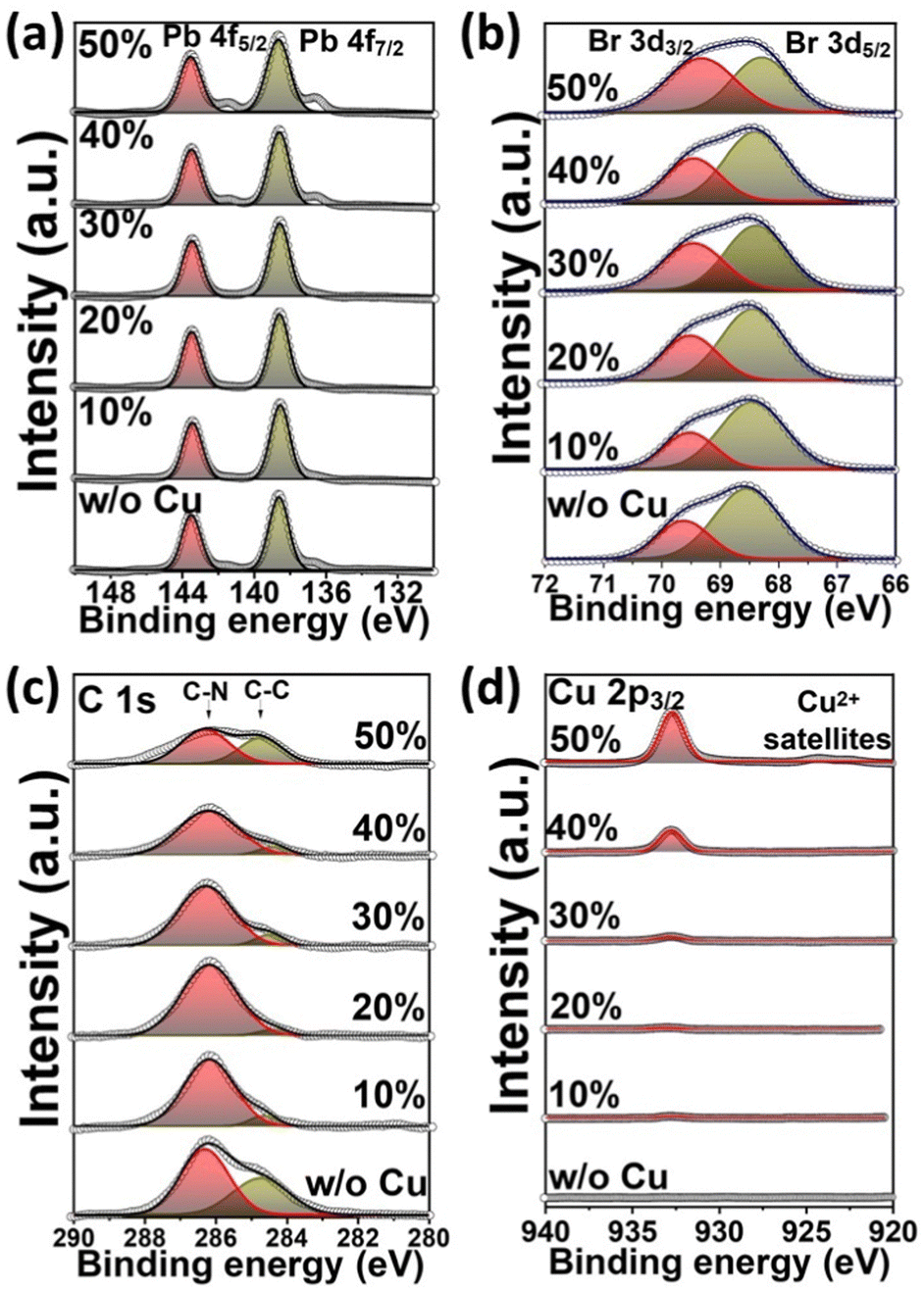 | ||
| Fig. 4 XPS spectra of Pb4f (a), Br3d (b), C1s (c), and Cu2p (d), and Br3d (e) of Cu-alloyed MAPbBr3 perovskite thin films. | ||
The optical properties of the samples are evaluated by obtaining UV-Vis absorption spectra of the pristine and Cu-substituted MAPbBr3 thin films (as illustrated in Fig. 5a). The absorption edges undergo a slight red-shifting with alloying of up to 40% Cu, and subsequently, a sudden and considerable red-shift (near-IR range) occurs for the 50% Cu-substituted sample. Tauc plots, Fig. 5b, and Fig. S10 (ESI†), show that the optical direct bandgaps of the perovskites are 2.32 eV for pristine MAPbBr3, 2.31 eV for 10%, 2.31 eV for 20%, 2.29 eV for 30%, 2.28 eV for 40%, and 1.85 eV for 50% Cu-substituted MAPbBr3 thin films. Tuning of the optical bandgap energies is consistent with the perovskite thin film color tuning (from yellowish orange to dark brown) with increasing Cu content. Moreover, the trend observed for the absorption spectrum of the 50% Cu-substituted film is similar to that observed for Cu-based perovskite materials.70 This may have resulted from the higher concentration of Cu-rich secondary phase in the 50% Cu-substituted film compared with the concentrations occurring in the other films. The inhomogeneous broadening of PL emission peaks with Cu-doping, as shown in Fig. S11a (ESI†), further confirms the heterogeneity of the doped films. The results revealed that 10% doping enhances room temperature PL emission of MAPbBr3 (76% increase in PL peak area), as shown in Fig. S11b (ESI†). This may have resulted from the homogeneously distributed low-Cu-concentration doping effect of the 10% Cu perovskite thin film without secondary phase formation. However, further Cu-doping (of up to 50% doping) leads to quenching of the PL emission and 85% recovery of the pristine MAPbBr3 PL emission (Fig. S11b, ESI†). Normalized PL spectra (Fig. S11c, ESI†) revealed that, with 50% Cu-doping, the PL shifts slightly (0.2 nm) to longer wavelength than those observed at other doping levels (Fig. S11d, ESI†).
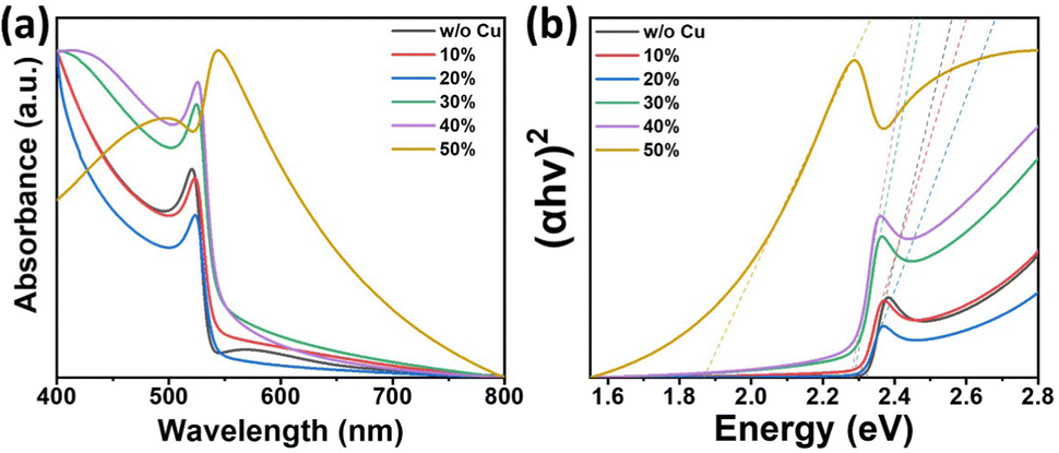 | ||
| Fig. 5 (a and b) Absorption spectra, and direct bandgap estimation: Tauc plot, respectively, of Cu-alloyed MAPbBr3 thin films. | ||
Using the four-probe method, we measured the electrical conductivity of perovskite thin films as a function of Cu alloying, as shown in Fig. 6a. The conductivity increases significantly with alloying and the highest value is obtained for the 40% Cu-substituted thin film, owing possibly to the presence of homogeneously distributed secondary phases. Subsequently, the conductivity decreases slightly for the 50% Cu substituted material, consistent with the heterogeneously distributed Cu-rich new phase formed in this material (as depicted in Fig. 2f and Fig. S2, ESI†). The 40% Cu-substituted MAPbBr3 thin film exhibits the highest dark electrical conductivity (10.77 × 10⁻⁴ S cm−1), which is nearly three orders of magnitude higher than that of the pristine MAPbBr3 thin film (4.10 × 10⁻⁷ S cm−1). To evaluate the secondary phase stability, we measure the conductivity under the effect of temperature (temperature range: 300 K–110 K) for one cooling/heating (C/H) cycle. We first measure the conductivity upon cooling from room temperature (300 K) to 110 K, and then upon heating back from 110 K to 330 K. Fig. 6b shows the results of temperature-dependent conductivity measurements performed on pristine MAPbBr3 where the conductivity decreases from 7.05 × 10⁻⁸ S cm−1 at 300 K to 2.72 × 10⁻⁸ S cm−1 at 110 K. The reverse behavior is observed upon heating, i.e., increasing conductivity with slight hysteresis at temperatures ranging from 200 K to 220 K. This behavior may have resulted from a phase transition where the tetragonal structure at T < 200 K transforms into a cubic structure at T > 220 K.71Fig. 6c shows the results of the conductivity measurements performed on 40% Cu-MAPbBr3. The conductivity decreases sharply from 1.16 × 10⁻³ S cm−1 at 300 K to 2.06 × 10⁻⁷ S cm−1 at 270 K and then decreases to 4.47 × 10⁻⁸ S cm−1 at 110 K. Interestingly, upon heating, the 40% Cu sample behave like pristine MAPbBr3 where the conductivity increases slightly to 2.66 × 10⁻⁷ S cm−1 at 330 K. The cooling/heating cycle behavior of the 40% Cu samples can be attributed to a phase transition from the secondary hexagonal phase at room temperature (300 K) to the cubic phase at 270 K. The inset image shown in Fig. 6c reveals that, at temperatures of 200–220 K, the same hysteresis occurs as the pristine perovskite (Fig. 6b), thereby confirming the occurrence of another phase transition to the tetragonal structure at T < 200 K. The Cu-alloyed perovskite thin film recovers its original conductivity value (1.08 × 10⁻³ S cm−1) after three days (Fig. 6d). This indicates that, compared with the pristine material, the 40% Cu perovskite requires more time for re-formation of its more stable hexagonal secondary phase with its original higher conductivity value. The activation energy (Ea) can reflect the energy difference between the conduction band and the Fermi energy (or defect levels). Ea required for charge transport can be obtained from conductivity measurements based on the Arrhenius equation S = S0![[thin space (1/6-em)]](https://www.rsc.org/images/entities/char_2009.gif) exp(−Ea/kBT) where S, S0, kB, and T are the conductivity, a constant, the Boltzmann constant, and the absolute temperature, respectively. We obtained an Ea of 29 meV for pristine MAPbBr3 and a considerably lower estimated value of 2 meV for the 40% Cu-substituted perovskite, as depicted in Fig. S12 (ESI†). The reduced Ea required for the alloyed perovskite may correspond to the change in Fermi energy or arising defect levels. This suggests that the carrier density increases with Cu-alloying where the presence of hexagonal secondary phases may play a crucial role in Ea reduction. For additional insight into the temperature-dependent conductivity behavior, the phase transitions in the 40% Cu-substituted perovskite are further tracked during three consecutive days of XRD measurements. The main cubic MAPbBr3 cubic structure of the material is retained after one day of the (C/H) cycle (Fig. 6e). However, the XRD peak of the hexagonal secondary phase is shifted to lower 2θ than the initial values (Fig. 6f). This shifting is accompanied by the appearance of a peak at 2θ = 9.2°, which corresponds to two-dimensional (2D) MA2CuBr4 perovskite.64 Moreover, the XRD peak at 2θ = 14.3°, which is associated with the unreacted CuBr2, disappears after the (C/H) cycle, thereby further confirming the formation of 2D Cu-based perovskite. This formation may have led to the aforementioned sudden decrease in the conductivity of the alloyed sample after the one-day (C/H) cycle. With the progression of the measurement, the XRD peak intensity of the MA2CuBr4 perovskite decreases, and the peak intensity of the hexagonal secondary phase increases. The direct dependence of the XRD peak intensity ratio (Iphasetransitions/IMA2CuBr4) on time reveals that the hexagonal secondary phases are restored at the expense of 2D MA2CuBr4 perovskite (as depicted in Fig. S13, ESI†). Consequently, the original conductivity of the 40% Cu-substituted perovskite is restored after the three-day measurement period.
exp(−Ea/kBT) where S, S0, kB, and T are the conductivity, a constant, the Boltzmann constant, and the absolute temperature, respectively. We obtained an Ea of 29 meV for pristine MAPbBr3 and a considerably lower estimated value of 2 meV for the 40% Cu-substituted perovskite, as depicted in Fig. S12 (ESI†). The reduced Ea required for the alloyed perovskite may correspond to the change in Fermi energy or arising defect levels. This suggests that the carrier density increases with Cu-alloying where the presence of hexagonal secondary phases may play a crucial role in Ea reduction. For additional insight into the temperature-dependent conductivity behavior, the phase transitions in the 40% Cu-substituted perovskite are further tracked during three consecutive days of XRD measurements. The main cubic MAPbBr3 cubic structure of the material is retained after one day of the (C/H) cycle (Fig. 6e). However, the XRD peak of the hexagonal secondary phase is shifted to lower 2θ than the initial values (Fig. 6f). This shifting is accompanied by the appearance of a peak at 2θ = 9.2°, which corresponds to two-dimensional (2D) MA2CuBr4 perovskite.64 Moreover, the XRD peak at 2θ = 14.3°, which is associated with the unreacted CuBr2, disappears after the (C/H) cycle, thereby further confirming the formation of 2D Cu-based perovskite. This formation may have led to the aforementioned sudden decrease in the conductivity of the alloyed sample after the one-day (C/H) cycle. With the progression of the measurement, the XRD peak intensity of the MA2CuBr4 perovskite decreases, and the peak intensity of the hexagonal secondary phase increases. The direct dependence of the XRD peak intensity ratio (Iphasetransitions/IMA2CuBr4) on time reveals that the hexagonal secondary phases are restored at the expense of 2D MA2CuBr4 perovskite (as depicted in Fig. S13, ESI†). Consequently, the original conductivity of the 40% Cu-substituted perovskite is restored after the three-day measurement period.
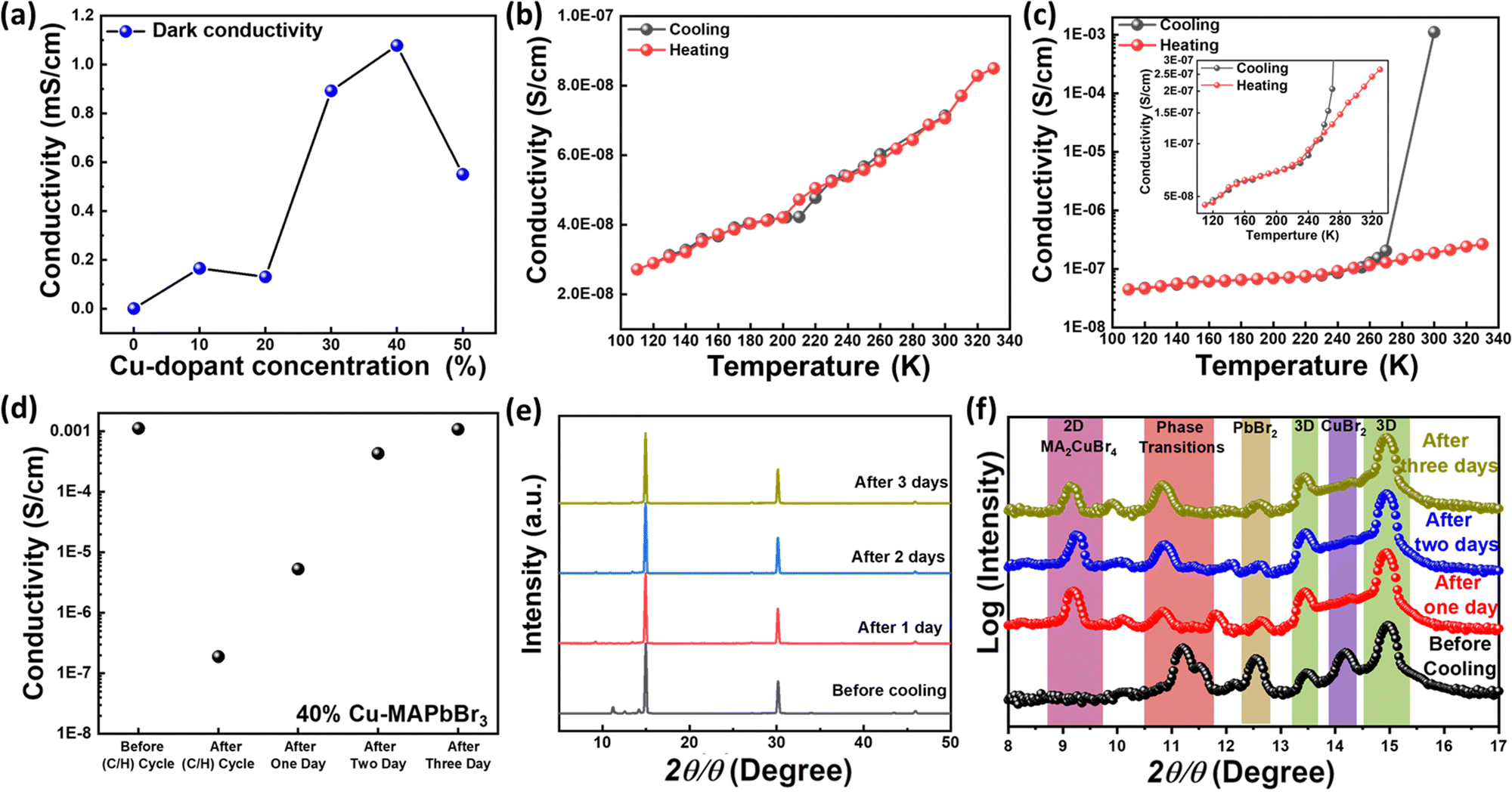 | ||
| Fig. 6 (a) Conductivity of Cu-MAPbBr3 perovskite thin films at room temperature. (b and c) Temperature-dependent conductivity of pristine MAPbBr3 and 40% Cu-MAPbBr3 perovskite thin films, respectively for one cooling/heating cycle. The inset in (c): zoom for low conductivity values. (d and e) Time-dependent conductivity and time-dependent XRD patterns, respectively, of 40% Cu-MAPbBr3 perovskite thin film after cooling/heating cycle effect. (f) Plots on log scale for 2θ = 8–17°. | ||
To determine the potential of pristine/alloyed perovskite thin films for optoelectronic devices, photocurrent measurements were performed as a function of the excitation wavelength (i.e., the excitation photon energy). Two types of transitions are (in general) observed (Fig. 7a): type I is a band-to-band transition (i.e., from valence band to conduction band), which requires higher excitation energy than the bandgap energy for photocarrier generation. Type II, which is a transition between a defect level and either the valence or conduction band, occurs with excitation energy either higher or lower than the bandgap energy for photocarrier generation.72Fig. 7b shows the normalized photocurrent spectra of both pristine and 40% Cu-substituted MAPbBr3 thin films as a function of the excitation photon energy. When the energy of excitation with photons is higher than the bandgap, EPh > Eg, the photocurrent of each sample rises sharply (i.e., intrinsic photocurrent generation occurs) despite the difference in alloying levels. Thereafter, the photocurrent decreases with increasing excitation photon energy. This may have resulted from the reduction in the penetration-depth (where carriers are generated at the perovskite surface), owing to rapid deterioration induced by the surface effect. It should be noted that, at higher energy, pristine perovskite reveals a higher surface recombination rate than that of 40% alloyed one, as shown in Fig. 7b, which might be due to the increasing of penetration depth upon Cu-alloying. No photocurrent generation occurs in pristine MAPbBr3 subjected to excitation at the near-infrared region. However, band-carrier generation increases with increasing Cu-substituting level. This strongly suggests that sub-bandgap absorption levels (defect levels) are present in the Cu-alloyed samples. Furthermore, defect level-related photocurrent is generated (i.e. Type II transition) above the threshold energy (ET), i.e., 1.25 eV (a defect level is located at ∼1.25 eV below the conduction band (or above the valence band)). This defect level behavior has been observed previously.72–75 The bandgaps of the perovskites are 2.24 eV for pristine MAPbBr3, and 2.22 eV, 2.19 eV, 2.14 eV, 1.90 eV, and 1.78 eV for 10%, 20%, 30%, 40%, and 50% Cu-substituted MAPbBr3 thin films, respectively (as depicted in Fig. S14, ESI†). These values correspond closely to the optical bandgaps obtained from the Tauc plots. Bandgap narrowing, with near IR carrier generation, makes Cu-alloyed MAPbBr3 perovskite thin film a promising candidate for NIR Photodetectors76 and other optoelectronic devices.77 It should be hinted that the only MAPbBr3 based photodetector, with narrow NIR-visible light dual-mode, was recently reported by Zhao et al.76
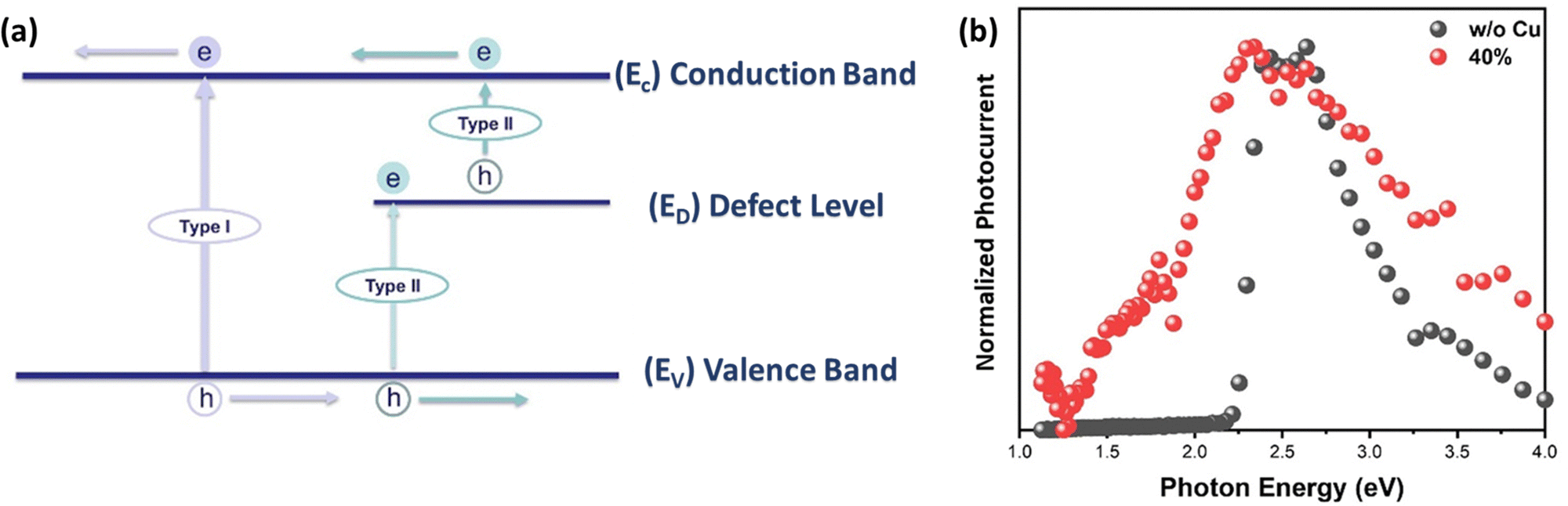 | ||
| Fig. 7 (a) Graphical illustration of photo-excitation processes in Cu-alloyed MAPbBr3 perovskite and (b) Photocurrent spectra of pristine MAPbBr3 and 40% Cu-alloyed MAPbBr3 thin films at room temperature. | ||
To gain further insight into Cu alloying of MAPbBr3, first principles point defect simulations were performed (details about the formalism are presented in ESI†). Here, we designate cubic MAPbBr3 as the parent phase and calculate the probability of CuPb extrinsic-defect formation. We employ a high Cu alloying concentration of 12.5% (5.59 × 10²⁰ atoms per cm3) in the model. The findings reported in the literature regarding the oxidation state of Cu substituted into halide perovskites are inconsistent72,78–81 (both +1 and +2 charge states have been reported). In our calculation, we consider both +1 (CuPb−1) and +2 (CuPb0) oxidation states of Cu, for modeling the Pb-replacing perovskite octahedra. The simulation results (Fig. 8a and b) revealed that, in the highly p-alloyed system (when the Fermi level is close to VBM), the neutral state is more stable than the other states. However, in the n-alloyed samples, Cu behaves as an acceptor type defect. Moreover, Cu substitution creates a charge imbalance in the system and can therefore trigger the formation of intrinsic secondary donor defects that compensate for this imbalance. The results reported in the literature indicate that, in the case of MAPbBr3, the most probable intrinsic donors are a Br vacancy (vBr) and an MA interstitial (MAi).82 Consequently, in this study, we consider CuPb, vBr, and MAi individual point defects as well as CuPb + vBr and CuPb + MAi defect complexes with different charge states. With Cu alloying, the octahedral geometry changes substantially (mainly due to size mismatch between Cu and Pb), and as such we consider Br vacancies at two different (namely axial and equatorial) sites of the octahedron. We incorporate the effect of chemical growth environment by considering the chemical potentials of the constituent elements.
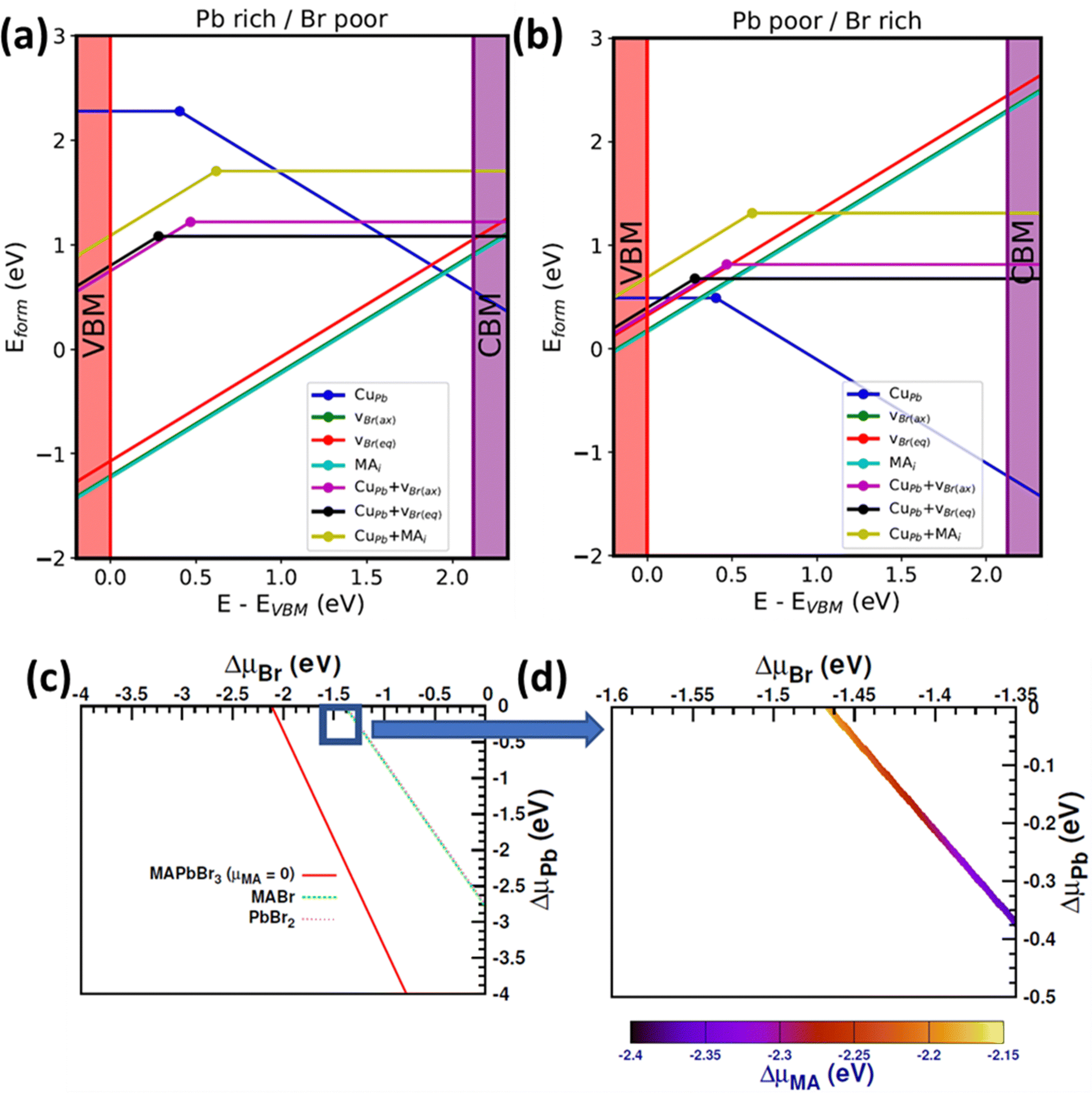 | ||
| Fig. 8 Formation energies of simulated point defects with respect to Fermi level associated with two different growth environments (Pb rich/Br poor (a) and Pb poor/Br rich (b)). Defect charge states (q) are the slope of the curves (we performed simulations for q = −1, 0, and +1) and charge transition points are denoted by circles. Red- and purple-shaded regions represent the valence band (and below) and conduction band (and above), respectively. (c) Compositional phase diagram showing competing secondary phases of MAPbBr3. (d) Zoomed view of the region enclosed in the box in (c). | ||
To elaborate, we draw a compositional phase diagram of MAPbBr3 (Fig. 8c and d) considering all the secondary phases from OQMD. We choose two corner points (chemical potential values to be used in defect formation energy calculation) of the diagram, which represent Pb rich/Br poor and Pb poor/Br rich conditions. The chemical potential of Cu is kept as rich as possible (for consistency with our experimental conditions) by considering elemental Cu and CuBr2 phases (experimental precursor) (additional details on the chosen chemical potential values are presented in the experimental section). To validate our methodology, we compare our calculated formation energies and charge transition levels of two intrinsic defects (namely vBr and MAi) with values reported in the literature, and a reasonable agreement is realized.83 The point defect diagrams (Fig. 8a and b) indicate that Cu alloying will be more likely under Pb poor/Br rich (p-type) growth conditions than under Pb rich/Br poor growth conditions. It is likely that the Fermi level pinning will be near CBM (VBM) under Pb rich/Br poor (Pb poor/Br rich) conditions. In this case, the formation energy of compensating intrinsic defects and defect complexes remains close to that of CuPb in both chemical environments. This means that defect compensation is likely for Cu alloying under these conditions. From our analysis, vBr turns out to be the most probable compensating defect. We also calculate the defect complex binding energy (Eb = Eform(CuPb + vBr) − Eform(CuPb) − Eform(vBr)) at different Fermi levels. Our calculated value lies between −0.41 eV (EF at VBM) and −0.53 eV (EF at CBM), indicating that formation of the CuPb + vBr defect complex is quite likely. However, for CuPb + MAi, Eb lies between 0.04 eV (EF at VBM) and 0.26 eV (EF at CBM), suggesting a moderate to low formation tendency of this complex. Moderate to deep-level (0.2–0.5 eV above VBM) charge transitions are observed for CuPb and the associated defect complexes.
We evaluate the effect of Cu alloying (and possible defect complexes) on the electronic properties of MAPbBr3 by plotting the orbital projected density of states for 50% Cu substituted MAPbBr3 with (and without) a Br vacancy, as shown in Fig. 9. With only Cu alloying at Pb sites, Fig. 9b, we observe that the effective gap decreases slightly (from 2.12 eV to 1.90 eV) compared with that of the pristine material, as depicted in Fig. 9a. In Fig. 9c, with the formation of Br vacancy (CuPb + vBr, defect complex), the presence of localized defect states can be observed within the pristine bandgap, formed by Cu-d and Br-p orbitals. This may explain the experimentally observed sub-bandgap absorption with 40% Cu alloying (Fig. 7b).
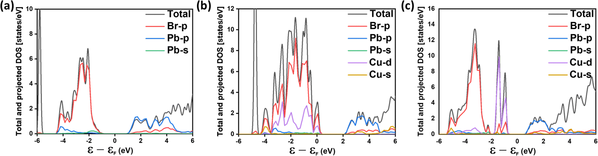 | ||
| Fig. 9 Atomic orbital projected density of states for (a) pure MAPbBr3, (b) 50% Cu alloyed MAPbBr3, and (c) 50% Cu alloyed MAPbBr3 with a Br vacancy. | ||
Experimental
Characterization
Scanning electron microscopy (SEM) with energy dispersive spectroscopy (EDS; JEOL, JEM-2100F) was used to determine the Pb/Cu atomic weight percentages and to obtain the elemental mapping of the perovskite samples. The results confirmed that the number of grain boundaries increased, and a Cu-rich secondary phase formed during Cu doping. The photoluminescence of the perovskite was characterized via Raman spectroscopy (JASCO, NRS4500 NMDS) performed with 532-nm excitation (green) lasers. Absorption measurements performed via ultraviolet-visible near-infrared (UV-Vis-NIR) spectroscopy (JASCO, V-670) were used to estimate the bandgap from a Tauc plot. X-ray (Rigaku XRD) reflection data was measured at a wavelength of 1.5406 Å. X-ray photoelectron spectroscopy (XPS) was characterized on JEOL JPS-9030 with X-ray source of Mg K Alfa (Monochromatic) with 25 mA beam current and 12 kV. In addition, electrical measurements were conducted using a source meter (ADCMT, 6245) with a temperature controller installed in a four-probe station (Riko International Ltd.). The sample temperature was controlled by cooling the sample stage of the four-probe station using liquid nitrogen with a temperature controller under vacuum condition (∼5.0 × 10⁻² Pa). Photocurrent measurements at room temperature were performed in the station using a source meter (KEITHLEY, 2611A) with monochromatic light illumination. The wavelength of this illumination was controlled by a monochromator (BUNKOKEIKI, SM2-25).Computational details
First-principles calculations were performed using Density Functional Theory (DFT)84 within the Projector-Augmented Wave (PAW)85 formalism as implemented in a GPAW86 code combined with an Atomic Simulation Environment (ASE).87 A plane wave cutoff energy of 800 eV and k-point density of 6 Å−1 (12 Å−1) were employed for geometry optimization (ground state calculations). Electronic structure calculations were performed using a Perdew–Burke–Ernzerhof (PBE)88 exchange–correlation functional. In addition, a 2 × 2 × 2 (96 atoms) supercell of the MAPbBr3 cubic unit cell was used for point defect calculations. A k-point density of 3.5 Å−1 (7 Å−1) was used for sampling the Brillouin zone for the supercells. Forces were converged up to 0.02 eV Å−1 for the defect calculations, where the supercell size was kept fixed. Compositional phase diagrams were obtained using a CPLAP code.89 The computational workflow was constructed using the Atomic Simulation Recipes (ASR)90 and executed using the My Queue91 task scheduler frontend.Conclusions
We have demonstrated that Cu alloying of MAPbBr3 thin films leads to an increase in the grain boundary area with the formation of Cu-rich secondary phases. The formation of hexagonal perovskite secondary phases is proposed to be more likely in the Cu-alloyed materials than in the non-alloyed materials as supported by calculated convex hull energies. Bandgap decreases slightly with Cu alloying until 40% concentration. A substantially reduced bandgap is observed in 50% Cu-substituted thin film which can be attributed to the presence of Cu-rich secondary phase. Intriguingly, the activation energy of the 40%Cu-substituted perovskite is considerably lower than that of the pristine material, and the conductivity is significantly higher (103×). In addition, photocurrent carriers are generated in the NIR region of the alloyed material. Based on point defect simulation results, we propose that a compensating Br vacancy will form with alloying and the associated defect complex may induce defect states inside the pristine bandgap, which may explain the experimentally observed optical signature.Author contributions
Amr Elattar conceived the manuscript's concept and designed the experiments. Amr Elattar, Kodai Nakao, and Kosei Tsutsumi synthesized the materials and conducted structural, electrical, and optical characterizations. Theoretical part was performed and wrote by Jiban Kangsabanik. The first manuscript was written by Amr Elattar and. At various phases, the writers discussed the findings and provided feedback on the manuscript. Kristian S. Thygesen led the assessment of theoretical part. Yasuhiko Hayashi coordinated the entire project.Conflicts of interest
There are no conflicts to declare.Acknowledgements
A. Elattar acknowledges the financial support from the Ministry of Higher Education, Egypt for his PhD scholarship (EJEP). We would like to thank Enago (https://www.enago.com/) for their English language editing service.References
- S. D. Stranks, G. E. Eperon, G. Grancini, C. Menelaou, M. J. P. Alcocer, T. Leijtens, L. M. Herz, A. Petrozza and H. J. Snaith, Electron-Hole Diffusion Lengths Exceeding 1 Micrometer in an Organometal Trihalide Perovskite Absorber, Science, 2013, 342, 341 LP–344 LP CrossRef PubMed.
- N. J. Jeon, J. H. Noh, Y. C. Kim, W. S. Yang, S. Ryu and S. Il, Seok, Solvent engineering for high-performance inorganic–organic hybrid perovskite solar cells, Nat. Mater., 2014, 13, 897–903 CrossRef CAS PubMed.
- N. J. Jeon, J. H. Noh, W. S. Yang, Y. C. Kim, S. Ryu, J. Seo and S. Il, Seok, Compositional engineering of perovskite materials for high-performance solar cells, Nature, 2015, 517, 476–480 CrossRef CAS PubMed.
- T. Chen, W.-L. Chen, B. J. Foley, J. Lee, J. P. C. Ruff, J. Y. P. Ko, C. M. Brown, L. W. Harriger, D. Zhang, C. Park, M. Yoon, Y.-M. Chang, J. J. Choi and S.-H. Lee, Origin of long lifetime of band-edge charge carriers in organic–inorganic lead iodide perovskites, Proc. Natl. Acad. Sci. U. S. A., 2017, 114, 7519 LP–7524 LP CrossRef PubMed.
- X. Yang, Y. Fu, R. Su, Y. Zheng, Y. Zhang, W. Yang, M. Yu, P. Chen, Y. Wang, J. Wu, D. Luo, Y. Tu, L. Zhao, Q. Gong and R. Zhu, Superior Carrier Lifetimes Exceeding 6 μs in Polycrystalline Halide Perovskites, Adv. Mater., 2020, 32, 2002585 CrossRef CAS PubMed.
- L. Qiao, W.-H. Fang, R. Long and O. V. Prezhdo, Photoinduced Dynamics of Charge Carriers in Metal Halide Perovskites from an Atomistic Perspective, J. Phys. Chem. Lett., 2020, 11, 7066–7082 CrossRef CAS PubMed.
- W. Li, A. S. Vasenko, J. Tang and O. V. Prezhdo, Anharmonicity Extends Carrier Lifetimes in Lead Halide Perovskites at Elevated Temperatures, J. Phys. Chem. Lett., 2019, 10, 6219–6226 CrossRef CAS PubMed.
- J. Jiang, X. Sun, X. Chen, B. Wang, Z. Chen, Y. Hu, Y. Guo, L. Zhang, Y. Ma, L. Gao, F. Zheng, L. Jin, M. Chen, Z. Ma, Y. Zhou, N. P. Padture, K. Beach, H. Terrones, Y. Shi, D. Gall, T.-M. Lu, E. Wertz, J. Feng and J. Shi, Carrier lifetime enhancement in halide perovskite via remote epitaxy, Nat. Commun., 2019, 10, 4145 CrossRef PubMed.
- E. L. Unger, L. Kegelmann, K. Suchan, D. Sörell, L. Korte and S. Albrecht, Roadmap and roadblocks for the band gap tunability of metal halide perovskites, J. Mater. Chem. A, 2017, 5, 11401–11409 RSC.
- Y. El Ajjouri, A. M. Igual-Muñoz, M. Sessolo, F. Palazon and H. J. Bolink, Tunable Wide-Bandgap Monohalide Perovskites, Adv. Opt. Mater., 2020, 8, 2000423 CrossRef CAS.
- R. J. Sutton, G. E. Eperon, L. Miranda, E. S. Parrott, B. A. Kamino, J. B. Patel, M. T. Hörantner, M. B. Johnston, A. A. Haghighirad, D. T. Moore and H. J. Snaith, Bandgap-Tunable Cesium Lead Halide Perovskites with High Thermal Stability for Efficient Solar Cells, Adv. Energy Mater., 2016, 6, 1502458 CrossRef.
- L. Wang, G. D. Yuan, R. F. Duan, F. Huang, T. B. Wei, Z. Q. Liu, J. X. Wang and J. M. Li, Tunable bandgap in hybrid perovskite CH3NH3Pb(Br3−yXy) single crystals and photodetector applications, AIP Adv., 2016, 6, 45115 CrossRef.
- Z. Yang, Z. Yu, H. Wei, X. Xiao, Z. Ni, B. Chen, Y. Deng, S. N. Habisreutinger, X. Chen, K. Wang, J. Zhao, P. N. Rudd, J. J. Berry, M. C. Beard and J. Huang, Enhancing electron diffusion length in narrow-bandgap perovskites for efficient monolithic perovskite tandem solar cells, Nat. Commun., 2019, 10, 4498 CrossRef PubMed.
- G. D. Tainter, M. T. Hörantner, L. M. Pazos-Outón, R. D. Lamboll, H. Āboliņš, T. Leijtens, S. Mahesh, R. H. Friend, H. J. Snaith, H. J. Joyce and F. Deschler, Long-Range Charge Extraction in Back-Contact Perovskite Architectures via Suppressed Recombination, Joule, 2019, 3, 1301–1313 CrossRef CAS.
- K. K. Chauhan, S. Prodhan, D. Ghosh, P. Waghale, S. Bhattacharyya, P. K. Dutta and P. K. Datta, Long Carrier Diffusion Length and Slow Hot Carrier Cooling in Thin Film Mixed Halide Perovskite, IEEE J. Photovolt., 2020, 10, 803–810 Search PubMed.
- M. C. Gélvez-Rueda, M. B. Fridriksson, R. K. Dubey, W. F. Jager, W. van der Stam and F. C. Grozema, Overcoming the exciton binding energy in two-dimensional perovskite nanoplatelets by attachment of conjugated organic chromophores, Nat. Commun., 2020, 11, 1901 CrossRef PubMed.
- K. Galkowski, A. Mitioglu, A. Miyata, P. Plochocka, O. Portugall, G. E. Eperon, J. T.-W. Wang, T. Stergiopoulos, S. D. Stranks, H. J. Snaith and R. J. Nicholas, Determination of the exciton binding energy and effective masses for methylammonium and formamidinium lead tri-halide perovskite semiconductors, Energy Environ. Sci., 2016, 9, 962–970 RSC.
- M. Baranowski and P. Plochocka, Excitons in Metal-Halide Perovskites, Adv. Energy Mater., 2020, 10, 1903659 CrossRef CAS.
- X. Chen, H. Lu, Y. Yang and M. C. Beard, Excitonic Effects in Methylammonium Lead Halide Perovskites, J. Phys. Chem. Lett., 2018, 9, 2595–2603 CrossRef CAS PubMed.
- C. Zhang, Y. Wang, X. Lin, T. Wu, Q. Han, Y. Zhang and L. Han, Effects of A site doping on the crystallization of perovskite films, J. Mater. Chem. A, 2021, 9, 1372–1394 RSC.
- M. Qin, H. Xue, H. Zhang, H. Hu, K. Liu, Y. Li, Z. Qin, J. Ma, H. Zhu, K. Yan, G. Fang, G. Li, U.-S. Jeng, G. Brocks, S. Tao and X. Lu, Precise Control of Perovskite Crystallization Kinetics via Sequential A-Site Doping, Adv. Mater., 2020, 32, 2004630 CrossRef CAS PubMed.
- S. Xu, X. Ding, H. Shi, X. Zhang, X. Sun, N. Ji, X. Zhang and Z. Zhang, EA-Directing Formamidinium-Based Perovskite Microwires with A-Site Doping, ACS Omega, 2021, 6, 7157–7164 CrossRef CAS PubMed.
- S. Wang, H. Liu, H. Bala, B. Zong, L. Huang, Z. Guo, W. Fu, B. Zhang, G. Sun, J. Cao and Z. Zhang, A highly stable hole-conductor-free CsxMA1-xPbI3 perovskite solar cell based on carbon counter electrode, Electrochim. Acta, 2020, 335, 135686 CrossRef CAS.
- T. Binyamin, L. Pedesseau, S. Remennik, A. Sawahreh, J. Even and L. Etgar, Fully Inorganic Mixed Cation Lead Halide Perovskite Nanoparticles: A Study at the Atomic Level, Chem. Mater., 2020, 32, 1467–1474 CrossRef CAS.
- D. P. McMeekin, G. Sadoughi, W. Rehman, G. E. Eperon, M. Saliba, M. T. Hörantner, A. Haghighirad, N. Sakai, L. Korte, B. Rech, M. B. Johnston, L. M. Herz and H. J. Snaith, A mixed-cation lead mixed-halide perovskite absorber for tandem solar cells, Science, 2016, 351, 151 LP–155 LP CrossRef PubMed.
- W. Rehman, D. P. McMeekin, J. B. Patel, R. L. Milot, M. B. Johnston, H. J. Snaith and L. M. Herz, Photovoltaic mixed-cation lead mixed-halide perovskites: links between crystallinity, photo-stability and electronic properties, Energy Environ. Sci., 2017, 10, 361–369 RSC.
- D. J. Kubicki, D. Prochowicz, A. Hofstetter, S. M. Zakeeruddin, M. Grätzel and L. Emsley, Phase Segregation in Potassium-Doped Lead Halide Perovskites from 39K Solid-State NMR at 21.1 T, J. Am. Chem. Soc., 2018, 140, 7232–7238 CrossRef CAS PubMed.
- Y. Zhou, J. Chen, O. M. Bakr and H.-T. Sun, Metal-Doped Lead Halide Perovskites: Synthesis, Properties, and Optoelectronic Applications, Chem. Mater., 2018, 30, 6589–6613 CrossRef CAS.
- Z. Tang, T. Bessho, F. Awai, T. Kinoshita, M. M. Maitani, R. Jono, T. N. Murakami, H. Wang, T. Kubo, S. Uchida and H. Segawa, Hysteresis-free perovskite solar cells made of potassium-doped organometal halide perovskite, Sci. Rep., 2017, 7, 12183 CrossRef PubMed.
- Q. Liu, M.-G. Ju and W. Liang, Potassium doping-induced variations in the structures and photoelectric properties of a MAPbI3 perovskite and a MAPbI3/TiO2 junction, Phys. Chem. Chem. Phys., 2020, 22, 20553–20561 RSC.
- B. Luo, F. Li, K. Xu, Y. Guo, Y. Liu, Z. Xia and J. Z. Zhang, B-Site doped lead halide perovskites: synthesis, band engineering, photophysics, and light emission applications, J. Mater. Chem. C, 2019, 7, 2781–2808 RSC.
- X. Ge, X. Qu, L. He, Y. Sun, X. Guan, Z. Pang, C. Wang, L. Yang, F. Wang and F. Rosei, 3D low toxicity Cu–Pb binary perovskite films and their photoluminescent/photovoltaic performance, J. Mater. Chem. A, 2019, 7, 27225–27235 RSC.
- J. Zhang, X. Gan, H. Sun, H. Yuan, L. Yu, Z. Hu and Y. Zhu, Pb-Site Doping of Lead Halide Perovskites for Efficient Solar Cells, Sol. RRL, 2020, 4, 1900227 CrossRef CAS.
- W. Liu, L. Chu, N. Liu, Y. Ma, R. Hu, Y. Weng, H. Li, J. Zhang, X. Li and W. Huang, Efficient perovskite solar cells fabricated by manganese cations incorporated in hybrid perovskites, J. Mater. Chem. C, 2019, 7, 11943–11952 RSC.
- M. N. Islam, M. A. Hadi and J. Podder, Influence of Ni doping in a lead-halide and a lead-free halide perovskites for optoelectronic applications, AIP Adv., 2019, 9, 125321 CrossRef.
- S. Thawarkar, P. J. S. Rana, R. Narayan and S. P. Singh, Ni-Doped CsPbBr3 Perovskite: Synthesis of Highly Stable Nanocubes, Langmuir, 2019, 35, 17150–17155 CrossRef CAS PubMed.
- S.-H. Chan, M.-C. Wu, K.-M. Lee, W.-C. Chen, T.-H. Lin and W.-F. Su, Enhancing perovskite solar cell performance and stability by doping barium in methylammonium lead halide, J. Mater. Chem. A, 2017, 5, 18044–18052 RSC.
- A. M. Ulatowski, A. D. Wright, B. Wenger, L. R. V. Buizza, S. G. Motti, H. J. Eggimann, K. J. Savill, J. Borchert, H. J. Snaith, M. B. Johnston and L. M. Herz, Charge-Carrier Trapping Dynamics in Bismuth-Doped Thin Films of MAPbBr3 Perovskite, J. Phys. Chem. Lett., 2020, 11, 3681–3688 CrossRef CAS PubMed.
- A. L. Abdelhady, M. I. Saidaminov, B. Murali, V. Adinolfi, O. Voznyy, K. Katsiev, E. Alarousu, R. Comin, I. Dursun, L. Sinatra, E. H. Sargent, O. F. Mohammed and O. M. Bakr, Heterovalent Dopant Incorporation for Bandgap and Type Engineering of Perovskite Crystals, J. Phys. Chem. Lett., 2016, 7, 295–301 CrossRef CAS PubMed.
- R. Meng, G. Wu, J. Zhou, H. Zhou, H. Fang, M. A. Loi and Y. Zhang, Understanding the Impact of Bismuth Heterovalent Doping on the Structural and Photophysical Properties of CH3NH3PbBr3 Halide Perovskite Crystals with Near-IR Photoluminescence, Chem. – Eur. J., 2019, 25, 5480–5488 CrossRef CAS PubMed.
- K. Yamada, H. Sera, S. Sawada, H. Tada, T. Okuda and H. Tanaka, Reconstructive Phase Transformation and Kinetics of Cs3Sb2I9 by Means of Rietveld Analysis of X-Ray Diffraction and 127I NQR, J. Solid State Chem., 1997, 134, 319–325 CrossRef CAS.
- M. Yavari, F. Ebadi, S. Meloni, Z. S. Wang, T. C.-J. Yang, S. Sun, H. Schwartz, Z. Wang, B. Niesen, J. Durantini, P. Rieder, K. Tvingstedt, T. Buonassisi, W. C. H. Choy, A. Filippetti, T. Dittrich, S. Olthof, J.-P. Correa-Baena and W. Tress, How far does the defect tolerance of lead-halide perovskites range? The example of Bi impurities introducing efficient recombination centers, J. Mater. Chem. A, 2019, 7, 23838–23853 RSC.
- Y. Yamada, M. Hoyano, R. Akashi, K. Oto and Y. Kanemitsu, Impact of Chemical Doping on Optical Responses in Bismuth-Doped CH3NH3PbBr3 Single Crystals: Carrier Lifetime and Photon Recycling, J. Phys. Chem. Lett., 2017, 8, 5798–5803 CrossRef CAS PubMed.
- S. Rong, Y. Xiao, J. Jiang, Q. Zeng and Y. Li, Strongly Enhanced Photoluminescence and Photoconductivity in Erbium-Doped MAPbBr3 Single Crystals, J. Phys. Chem. C, 2020, 124, 8992–8998 CrossRef CAS.
- J. Gong, M. Yang, D. Rebollar, J. Rucinski, Z. Liveris, K. Zhu and T. Xu, Divalent Anionic Doping in Perovskite Solar Cells for Enhanced Chemical Stability, Adv. Mater., 2018, 30, 1800973 CrossRef PubMed.
- M. Karlsson, Z. Yi, S. Reichert, X. Luo, W. Lin, Z. Zhang, C. Bao, R. Zhang, S. Bai, G. Zheng, P. Teng, L. Duan, Y. Lu, K. Zheng, T. Pullerits, C. Deibel, W. Xu, R. Friend and F. Gao, Mixed halide perovskites for spectrally stable and high-efficiency blue light-emitting diodes, Nat. Commun., 2021, 12, 361 CrossRef CAS PubMed.
- H. F. Zarick, N. Soetan, W. R. Erwin and R. Bardhan, Mixed halide hybrid perovskites: a paradigm shift in photovoltaics, J. Mater. Chem. A, 2018, 6, 5507–5537 RSC.
- P. Nandi, Z. Li, Y. Kim, T. K. Ahn, N.-G. Park and H. Shin, Stabilizing Mixed Halide Lead Perovskites against Photoinduced Phase Segregation by A-Site Cation Alloying, ACS Energy Lett., 2021, 6, 837–847 CrossRef CAS.
- Z. Chen, G. Brocks, S. Tao and P. A. Bobbert, Unified theory for light-induced halide segregation in mixed halide perovskites, Nat. Commun., 2021, 12, 2687 CrossRef CAS PubMed.
- L. Lei, Q. Dong, K. Gundogdu and F. So, Metal Halide Perovskites for Laser Applications, Adv. Funct. Mater., 2021, 31, 2010144 CrossRef CAS.
- S. Das, S. Gholipour and M. Saliba, Perovskites for Laser and Detector Applications, Energy Environ. Mater., 2019, 2, 146–153 CrossRef.
- T. S. Kao, Y.-H. Hong, K.-B. Hong and T.-C. Lu, Perovskite random lasers: a tunable coherent light source for emerging applications, Nanotechnology, 2021, 32, 282001 CrossRef CAS PubMed.
- W. Sun, Y. Liu, G. Qu, Y. Fan, W. Dai, Y. Wang, Q. Song, J. Han and S. Xiao, Lead halide perovskite vortex microlasers, Nat. Commun., 2020, 11, 4862 CrossRef CAS PubMed.
- H. Jing, R. Peng, R.-M. Ma, J. He, Y. Zhou, Z. Yang, C.-Y. Li, Y. Liu, X. Guo, Y. Zhu, D. Wang, J. Su, C. Sun, W. Bao and M. Wang, Flexible Ultrathin Single-Crystalline Perovskite Photodetector, Nano Lett., 2020, 20, 7144–7151 CrossRef CAS PubMed.
- C. Li, H. Wang, F. Wang, T. Li, M. Xu, H. Wang, Z. Wang, X. Zhan, W. Hu and L. Shen, Ultrafast and broadband photodetectors based on a perovskite/organic bulk heterojunction for large-dynamic-range imaging, Light: Sci. Appl., 2020, 9, 31 CrossRef CAS PubMed.
- J. Deng, J. Xun, Y. Qin, M. Li and R. He, Blue-emitting NH4+-doped MAPbBr3 perovskite quantum dots with near unity quantum yield and super stability, Chem. Commun., 2020, 56, 11863–11866 RSC.
- R. Li, S. Chen, X. Li, G. Yin, Y. Gong, J. Yu, G. Pang, J. Liu, Y. Liu, Z. Ni, L. Zhang, R. Chen and H.-L. Wang, Zn doped MAPbBr3 single crystal with advanced structural and optical stability achieved by strain compensation, Nanoscale, 2020, 12, 3692–3700 RSC.
- Y. Yamada, M. Hoyano, K. Oto and Y. Kanemitsu, Effects of Impurity Doping on Photoluminescence Properties of APbX3 Lead Halide Perovskites, Phys. Status Solidi B, 2019, 256, 1800545 CrossRef.
- C. C. Stoumpos, C. D. Malliakas and M. G. Kanatzidis, Semiconducting Tin and Lead Iodide Perovskites with Organic Cations: Phase Transitions, High Mobilities, and Near-Infrared Photoluminescent Properties, Inorg. Chem., 2013, 52, 9019–9038 CrossRef CAS PubMed.
- P. Gratia, I. Zimmermann, P. Schouwink, J.-H. Yum, J.-N. Audinot, K. Sivula, T. Wirtz and M. K. Nazeeruddin, The Many Faces of Mixed Ion Perovskites: Unraveling and Understanding the Crystallization Process, ACS Energy Lett., 2017, 2, 2686–2693 CrossRef CAS.
- J. Tian, D. B. Cordes, A. M. Z. Slawin, E. Zysman-Colman and F. D. Morrison, Progressive Polytypism and Bandgap Tuning in Azetidinium Lead Halide Perovskites, Inorg. Chem., 2021, 60, 12247–12254 CrossRef CAS PubMed.
- L. S. Ramsdell, Studies on silicon carbide, Am. Mineral., 1947, 32, 64–82 CAS.
- K.-H. Wang, L.-C. Li, M. Shellaiah and K. Wen, Sun, Structural and Photophysical Properties of Methylammonium Lead Tribromide (MAPbBr3) Single Crystals, Sci. Rep., 2017, 7, 13643 CrossRef PubMed.
- A. Elattar, H. Suzuki, R. Mishima, K. Nakao, H. Ota, T. Nishikawa, H. Inoue, A. K. K. Kyaw and Y. Hayashi, Single crystal of two-dimensional mixed-halide copper-based perovskites with reversible thermochromism, J. Mater. Chem. C, 2021, 9, 3264–3270 RSC.
- J. E. Saal, S. Kirklin, M. Aykol, B. Meredig and C. Wolverton, Materials Design and Discovery with High-Throughput Density Functional Theory: The Open Quantum Materials Database (OQMD), JOM, 2013, 65, 1501–1509 CrossRef CAS.
- K. Lin, J. Xing, L. N. Quan, F. P. G. de Arquer, X. Gong, J. Lu, L. Xie, W. Zhao, D. Zhang, C. Yan, W. Li, X. Liu, Y. Lu, J. Kirman, E. H. Sargent, Q. Xiong and Z. Wei, Perovskite light-emitting diodes with external quantum efficiency exceeding 20 per cent, Nature, 2018, 562, 245–248 CrossRef CAS PubMed.
- P. Pandey, N. Sharma, R. A. Panchal, S. W. Gosavi and S. Ogale, Realization of High Capacity and Cycling Stability in Pb-Free A2CuBr4 (A = CH3NH3/Cs, 2D/3D) Perovskite-Based Li-Ion Battery Anodes, ChemSusChem, 2019, 12, 3742–3746 CrossRef CAS PubMed.
- P. Yang, G. Liu, B. Liu, X. Liu, Y. Lou, J. Chen and Y. Zhao, All-inorganic Cs2CuX4 (X = Cl, Br, and Br/I) perovskite quantum dots with blue-green luminescence, Chem. Commun., 2018, 54, 11638–11641 RSC.
- N. Li, C. Cheng, H. Wei, H. Liu, X. Li, W. Li and L. Wang, Enhanced efficiency and stability of inverted perovskite solar cells by interfacial engineering with alkyl bisphosphonic molecules, RSC Adv., 2017, 7, 42105–42112 RSC.
- D. Cortecchia, H. A. Dewi, J. Yin, A. Bruno, S. Chen, T. Baikie, P. P. Boix, M. Grätzel, S. Mhaisalkar, C. Soci and N. Mathews, Lead-Free MA2CuClxBr4–x Hybrid Perovskites, Inorg. Chem., 2016, 55, 1044–1052 CrossRef CAS PubMed.
- Y. Liu, H. Lu, J. Niu, H. Zhang, S. Lou, C. Gao, Y. Zhan, X. Zhang, Q. Jin and L. Zheng, Temperature-dependent photoluminescence spectra and decay dynamics of MAPbBr3 and MAPbI3 thin films, AIP Adv., 2018, 8, 95108 CrossRef.
- F. Ji, Y. Huang, F. Wang, L. Kobera, F. Xie, J. Klarbring, S. Abbrent, J. Brus, C. Yin, S. I. Simak, I. A. Abrikosov, I. A. Buyanova, W. M. Chen and F. Gao, Near-Infrared Light-Responsive Cu-Doped Cs2AgBiBr6, Adv. Funct. Mater., 2020, 30, 2005521 CrossRef CAS.
- C. B. Simmons, A. J. Akey, J. P. Mailoa, D. Recht, M. J. Aziz and T. Buonassisi, Enhancing the Infrared Photoresponse of Silicon by Controlling the Fermi Level Location within an Impurity Band, Adv. Funct. Mater., 2014, 24, 2852–2858 CrossRef CAS.
- J. P. Mailoa, A. J. Akey, C. B. Simmons, D. Hutchinson, J. Mathews, J. T. Sullivan, D. Recht, M. T. Winkler, J. S. Williams, J. M. Warrender, P. D. Persans, M. J. Aziz and T. Buonassisi, Room-temperature sub-band gap optoelectronic response of hyperdoped silicon, Nat. Commun., 2014, 5, 3011 CrossRef PubMed.
- M. K. Kavitha, K. B. Jinesh, R. Philip, P. Gopinath and H. John, Defect engineering in ZnO nanocones for visible photoconductivity and nonlinear absorption, Phys. Chem. Chem. Phys., 2014, 16, 25093–25100 RSC.
- J. Zhao, X. Wang, Y. Xu, Y. Pan, Y. Li, J. Chen, Q. Li, X. Zhang, Z. Zhu, Z. Zhao, E. E. Elemike, D. C. Onwudiwe, B. S. Bae, S. bin Shafie and W. Lei, Electrically Modulated Near-Infrared/Visible Light Dual-Mode Perovskite Photodetectors, ACS Appl. Mater. Interfaces, 2022, 14, 25824–25833 CrossRef CAS PubMed.
- N. J. Jeon, J. H. Noh, W. S. Yang, Y. C. Kim, S. Ryu, J. Seo and S. il Seok, Compositional engineering of perovskite materials for high-performance solar cells, Nature, 2015, 517, 476–480 CrossRef CAS PubMed.
- F. Chen, L. Xu, Y. Li, T. Fang, T. Wang, M. Salerno, M. Prato and J. Song, Highly efficient sky-blue light-emitting diodes based on Cu-treated halide perovskite nanocrystals, J. Mater. Chem. C, 2020, 8, 13445–13452 RSC.
- C. Bi, S. Wang, Q. Li, S. V. Kershaw, J. Tian and A. L. Rogach, Thermally Stable Copper(II)-Doped Cesium Lead Halide Perovskite Quantum Dots with Strong Blue Emission, J. Phys. Chem. Lett., 2019, 10, 943–952 CrossRef CAS PubMed.
- A. De, S. Das, N. Mondal and A. Samanta, Highly Luminescent Violet- and Blue-Emitting Stable Perovskite Nanocrystals, ACS Mater. Lett., 2019, 1, 116–122 CrossRef CAS.
- Y.-C. Chen, H.-L. Chou, J.-C. Lin, Y.-C. Lee, C.-W. Pao, J.-L. Chen, C.-C. Chang, R.-Y. Chi, T.-R. Kuo, C.-W. Lu and D.-Y. Wang, Enhanced Luminescence and Stability of Cesium Lead Halide Perovskite CsPbX3 Nanocrystals by Cu2+-Assisted Anion Exchange Reactions, J. Phys. Chem. C, 2019, 123, 2353–2360 CrossRef CAS.
- S. G. Motti, D. Meggiolaro, S. Martani, R. Sorrentino, A. J. Barker, F. De Angelis and A. Petrozza, Defect Activity in Lead Halide Perovskites, Adv. Mater., 2019, 31, 1901183 CrossRef CAS PubMed.
- A. Mannodi-Kanakkithodi, J. Park, D. H. Cao, N. Jeon, A. B. F. Martinson and M. K. Y. Chan, First-principles Study of Intrinsic and Extrinsic Point Defects in Lead-Based Hybrid Perovskites, in 2018 IEEE 7th World Conference on Photovoltaic Energy Conversion (WCPEC) (A Joint Conference of 45th IEEE PVSC, 28th PVSEC & 34th EU PVSEC), 2018, pp. 495–498 Search PubMed.
- W. Kohn and L. J. Sham, Self-Consistent Equations Including Exchange and Correlation Effects, Phys. Rev., 1965, 140, A1133–A1138 CrossRef.
- P. E. Blöchl, Projector augmented-wave method, Phys. Rev. B: Condens. Matter Mater. Phys., 1994, 50, 17953–17979 CrossRef PubMed.
- J. Enkovaara, C. Rostgaard, J. J. Mortensen, J. Chen, M. Dułak, L. Ferrighi, J. Gavnholt, C. Glinsvad, V. Haikola, H. A. Hansen, H. H. Kristoffersen, M. Kuisma, A. H. Larsen, L. Lehtovaara, M. Ljungberg, O. Lopez-Acevedo, P. G. Moses, J. Ojanen, T. Olsen, V. Petzold, N. A. Romero, J. Stausholm-Møller, M. Strange, G. A. Tritsaris, M. Vanin, M. Walter, B. Hammer, H. Häkkinen, G. K. H. Madsen, R. M. Nieminen, J. K. Nørskov, M. Puska, T. T. Rantala, J. Schiøtz, K. S. Thygesen and K. W. Jacobsen, Electronic structure calculations with GPAW: a real-space implementation of the projector augmented-wave method, J. Phys.: Condens. Matter, 2010, 22, 253202 CrossRef CAS PubMed.
- A. Hjorth Larsen, J. Jørgen Mortensen, J. Blomqvist, I. E. Castelli, R. Christensen, M. Dułak, J. Friis, M. N. Groves, B. Hammer, C. Hargus, E. D. Hermes, P. C. Jennings, P. Bjerre Jensen, J. Kermode, J. R. Kitchin, E. Leonhard Kolsbjerg, J. Kubal, K. Kaasbjerg, S. Lysgaard, J. Bergmann Maronsson, T. Maxson, T. Olsen, L. Pastewka, A. Peterson, C. Rostgaard, J. Schiøtz, O. Schütt, M. Strange, K. S. Thygesen, T. Vegge, L. Vilhelmsen, M. Walter, Z. Zeng and K. W. Jacobsen, The atomic simulation environment—a Python library for working with atoms, J. Phys.: Condens. Matter, 2017, 29, 273002 CrossRef PubMed.
- J. P. Perdew, K. Burke and M. Ernzerhof, Generalized Gradient Approximation Made Simple, Phys. Rev. Lett., 1996, 77, 3865–3868 CrossRef CAS PubMed.
- J. Buckeridge, D. O. Scanlon, A. Walsh and C. R. A. Catlow, Automated procedure to determine the thermodynamic stability of a material and the range of chemical potentials necessary for its formation relative to competing phases and compounds, Comput. Phys. Commun., 2014, 185, 330–338 CrossRef CAS.
- M. Gjerding, T. Skovhus, A. Rasmussen, F. Bertoldo, A. H. Larsen, J. J. Mortensen and K. S. Thygesen, Atomic Simulation Recipes: A Python framework and library for automated workflows, Comput. Mater. Sci., 2021, 199, 110731 CrossRef CAS.
- K. S. T. Jens Jørgen Mortensen and M. Gjerding, MyQueue: Task and workflow scheduling system, J. Open Source Softw., 2020, 45, 1844 CrossRef.
Footnote |
| † Electronic supplementary information (ESI) available. See DOI: https://doi.org/10.1039/d2qm00491g |
| This journal is © the Partner Organisations 2022 |