
Transparent photodetectors based on polyoxometalate modified electrospun ZnO homojunction nanowire intersection arrays†
Yuxiao
Zheng
a,
Xueying
Xu
a,
Fengrui
Li
a,
Weilin
Chen
 *a,
Jian
Gong
*a and
Chunlei
Wang
b
*a,
Jian
Gong
*a and
Chunlei
Wang
b
aKey Laboratory of Polyoxometalate and Reticular Material Chemistry of Ministry of Education, Faculty of Chemistry, Northeast Normal University, Changchun, 130024, China. E-mail: chenwl@nenu.edu.cn
bLibrary of Northeast Normal University, Changchun, 130024, China
First published on 6th November 2021
Abstract
Transparent photodetectors (PDs) based on binary metal oxides have become a hot topic in the field of photodetection because of their ability to absorb and detect ultraviolet (UV) light. However, PDs constructed with pure binary metal oxides still have the problems of slow response time and high-voltage drive. In addition, due to its natural internal defects, it has the characteristics of an n-type semiconductor and is difficult to achieve p-type conversion. In this work, the top layer of the device is polyoxometalate (POM) modified ZnO NWs which showed the characteristics of p-type semiconductors, its UV absorption was increased by 36.9%, and the bottom layer of the PD is pure ZnO NWs. An interlayer p–n junction is formed between the two layers, which is not only conducive to carrier transmission, but also can complete photodetection without bias. The PD has a transparency of more than 70% in the visible light region. Under the conditions of zero bias and AM 1.5 illumination, the light–dark current difference (ΔI) reaches 23.76 μA, and the rise-fall time is 1.32 s/2.62 s, respectively. After 216 hours of cycling, it still maintains 70% of the original efficiency.
1. Introduction
The harm of UV light to the human body is unquestionable. Although the UV light in the sunlight will be absorbed and reflected to a certain extent when the sunlight passes through the ozone layer, the human body is exposed to the sunlight for a long time, and there will still be a series of skin diseases caused by UV light.1–5 Therefore, how to shield the human body from UV light has received widespread attention, and designing PDs that absorb and detect UV light has gradually become a hot topic in the field of photoelectric detection.6–9 Among the PDs that absorb and detect UV light, low-latitude devices based on binary metal oxides (such as TiO2, ZnO, Ga2O3, etc.) exhibit a variety of excellent properties such as high responsiveness, rapid response time, and large carrier mobility.10–19As a typical wide band gap n-type semiconductor, zinc oxide (ZnO) has been applied in the field of UV photodetection due to its suitable energy band (Eg = 3.37 eV) and good optical properties.20 PDs based on pure ZnO low-latitude nanomaterials show good performance, but still have a long response time and the need for a high-voltage drive, which affect the continued promotion and application of ZnO-based PDs.21–23 In addition, as a wide band gap semiconductor, wurtzite-type ZnO has internal defects, making it an n-type semiconductor. It is difficult for this type of n-type semiconductor to achieve p-type conversion. Attempts have been made to construct p–n heterojunctions with other common p-type materials and ZnO, but the effect is not ideal due to the energy level mismatch.18,24–29 Researchers also tried to dope or modify ZnO with some materials to achieve p–n modification.30–40 However, the materials used are expensive and their difficulty to be widely applied is still an important problem.
POMs are a class of metal oxide clusters with nano-scale size, which have semiconductor-like characteristics, and they also have characteristics not found in general metal oxide semiconductors.41–50 First of all, POMs have an adjustable energy band, which can be adjusted well after being compounded with semiconductor materials. Secondly, POMs have good light absorption, especially strong absorption in the UV region, and after the semiconductor materials are combined, the absorbance of the composite material can be improved. Finally, after POMs are compounded with semiconductor materials, they can act as shallow electron traps, separating photogenerated excitons under illumination, and enhancing electron transmission. In view of the above characteristics, POMs have been applied to dye-sensitized solar cells (DSSCs) and perovskite solar cells (PSCs), proving that they have good application prospects in the field of optoelectronics.51–56
According to the characteristics of POMs, this work uses POMs to modify ZnO NWs for PDs, and completes the device preparation by electrospinning. POMs tend to agglomerate, so electrospinning is used to solve this problem.7,31,57 The three kinds of Keggin-type POMs selected in this work are Na8[HPW9O34] (PW9), Na7[PW11O39] (PW11) and H3[PW12O40] (PW12). They all have the function of adjusting the energy band.58–60 The Eg values of ZnO NWs modified by POMs have been changed. The UV-visible absorption spectra proved that after being combined with POMs, the UV absorption of the pure ZnO NWs had increased by 32.7% (PW9), 36.9% (PW11), and 20.1% (PW12), respectively. The top layer of PD is ZnO NWs modified with POMs. The Mott–Schottky curve proves that ZnO NWs modified with POMs exhibit the characteristics of p-type semiconductors. Through infrared (IR) spectroscopy, X-ray diffraction (XRD) and X-ray photoelectron spectroscopy (XPS), it is proved that POMs and ZnO NWs are more than simple physical doping. The bottom layer of the PD is formed by pure ZnO NWs, and a p–n homojunction is formed between the two layers of spinning to better complete the carrier transmission and make the PD work under unbiased conditions. The UV-visible transmission spectrum proves that the PD maintains a transparency of more than 70% in the visible light region. Under the working conditions of zero bias voltage and AM 1.5 illumination, the light–dark current difference (ΔI) reaches 23.76 μA, and the rise-fall time of PD is 1.32 s/2.62 s. After 216 hours of cycling, the PD still maintains 70% of the original efficiency.
2. Experimental
2.1 Preparation of materials
PW9, PW11 and PW12 were synthesized according to the literature reported previously, and the synthesis method was described in the ESI.† The materials required for the synthesis, including phosphoric acid (A.R.), sodium tungstate (A.R.), binary hydrogen phosphate (A.R.), glacial acetic acid (A.R.), concentrated nitric acid (A.R.) and acetone (A.R.), were purchased from Aladdin and have not been further purified.2.2 The precursor preparation method of pure ZnO NWs and POMs modified ZnO NWs
0.9 g of polyvinylpyrrolidone (PVP, Mn = 1![[thin space (1/6-em)]](https://www.rsc.org/images/entities/char_2009.gif) 300000) was dissolved in 15 g of ethanol and stirred at room temperature for 6 to 8 hours until the solution was completely clear and transparent. At the same time, 0.8 g of Zn(NO3)2·6H2O was dissolved in 2 g of deionized water and stirred for 15 min at room temperature to make it completely dissolved. Then the prepared zinc nitrate solution was added to the prepared PVP solution drop by drop, and stirred at room temperature for 8 h until the solution is completely mixed. For the precursor modified by POMs, the prepared POMs were added into a solution of zinc nitrate, and the mass doping ratios of PW9 were 1:10 and 1:20, the doping ratios of PW11 were 1:10, 1:20 and 1:50, and the doping ratio of PW12 was 1:15.
300000) was dissolved in 15 g of ethanol and stirred at room temperature for 6 to 8 hours until the solution was completely clear and transparent. At the same time, 0.8 g of Zn(NO3)2·6H2O was dissolved in 2 g of deionized water and stirred for 15 min at room temperature to make it completely dissolved. Then the prepared zinc nitrate solution was added to the prepared PVP solution drop by drop, and stirred at room temperature for 8 h until the solution is completely mixed. For the precursor modified by POMs, the prepared POMs were added into a solution of zinc nitrate, and the mass doping ratios of PW9 were 1:10 and 1:20, the doping ratios of PW11 were 1:10, 1:20 and 1:50, and the doping ratio of PW12 was 1:15.
2.3 Preparation of a PD and its working principle
The simulation schematic diagram of spinning is shown in Fig. 1a. By applying a positive high voltage of +10 kV to the needle, the spinning solution is extruded from the spinneret through the syringe pump to form droplets. Under the action of high voltage electricity, the droplet deformation occurs, and if the voltage is low, it will appear tapered. When the voltage further increases until it exceeds a certain critical value, under the excitation of the high voltage, the droplets form a jet. Through violent vibration in the air, the jet is stretched and refined. At this time, metal electrodes are placed at both ends of the collector. As shown in the right picture in Fig. 1a, the jet is fixed on the surface of the current collector in an orderly manner to achieve the goal of unidirectional rotation. The collector is FTO conductive glass, and the distance between the collector and the injection needle is 10 cm. | ||
| Fig. 1 (a) Schematic diagram of the simulation of the basic principle of electrospinning. (b) Schematic diagram of the simulation of the photodetector (not drawn to scale). (c) Schematic diagram of the reaction mechanism and energy band of the PW11@ZnO NWs/pure ZnO NWs p–n homojunction under 0 bias. | ||
Fig. 1b shows a schematic diagram of the entire device (not drawn to scale). The entire device has a vertical structure. FTO conductive glass was used as a collecting device. The bottom layer was spun with an undoped ZnO precursor and the top layer was doped with POMs. The precursor fluid controlled the direction of spinning of the two layers by changing the direction of the collector. The pure zinc nitrate precursor solution was used for bottom spinning, and the POM dissolved precursor solution was used for top spinning. After the spinning was complete, annealing was completed quickly at 550 °C. The photo of the obtained device is shown in Fig. S4 (ESI†). The light transmittance is shown in Fig. S5 (ESI†).
The simulation schematic diagram of the device for photodetection is shown in Fig. 1c. As seen in the figure, the valence band of PW11@ZnO NWs is 0.454 eV higher than that of pure ZnO NWs, and our PW11@ZnO/ZnO homojunction NWs have been cross-arranged, which formed a p–n homojunction structure. In this case, due to the generation of electron–hole pairs under the light, the electrons will move to the pure ZnO NW side, and the holes will move to the PW11@ZnO side, thereby helping in the formation of a charge transfer state, and conducive to the separation of light-generated carriers in NWs.
3. Results and discussion
Fig. 2a–c show the comparison of IR spectra of three pure POMs and POMs@ZnO NWs. Fig. 2a shows the IR spectra of pure ZnO NWs, pure PW11 and PW11@NWs. The characteristic peaks of the IR spectrum of PW11 are at 1099 cm−1 (P–O), 954 cm−1 (W![[double bond, length as m-dash]](https://www.rsc.org/images/entities/char_e001.gif) O), 897 cm−1 and 857 cm−1 (W–Ob–W), 812 cm−1 and 738 cm−1 (W–Oc–W), which belong to the stretching vibration peaks of the PW11 anion. This is consistent with the previously reported single-vacancy Keggin-type POM compounds.58 The characteristic peaks of PW11 can be observed in the IR spectrum of PW11@ZnO NWs, and the shift of these peak positions can be observed, indicating that there is an interaction between PW11 and ZnO.58,61,62Fig. 2b shows the IR spectra of pure PW9 and PW9@ZnO NWs. The characteristic peaks of the IR spectrum of PW9 are at 1059 cm−1 (P–O), 932 cm−1 (W–Ot), 880 cm−1 (W–Ob), 811 cm−1 and 729 cm−1 (W–Oc–W), which belong to the vibration peak of the PW9 anion, which is consistent with the previously reported multi-vacancy Keggin-type POM compound.59 The characteristic peaks of PW9 can be observed in the IR spectrum of PW9@ZnO NWs, and the shift of these peak positions can be observed, indicating that there is an interaction between PW9 and ZnO. Fig. 2c shows the IR spectra of pure PW12 and PW12@ZnO NWs. Among them, the characteristic peaks of the IR spectrum of PW12 are at 1074 cm−1, 973 cm−1, 902 cm−1 and 773 cm−1. These strong peaks are better than the stretching of the PO4 unit and W–O–W bond in PW12. The vibration is caused by the vibration peak belonging to the PW12 anion, which is consistent with the previously reported saturated Keggin-type POM compound.60 The characteristic peaks of PW12 can be observed in the IR spectrum of PW12@ZnO NWs, and the shift of these peak positions can be observed, indicating that there is an interaction between PW12 and ZnO.
O), 897 cm−1 and 857 cm−1 (W–Ob–W), 812 cm−1 and 738 cm−1 (W–Oc–W), which belong to the stretching vibration peaks of the PW11 anion. This is consistent with the previously reported single-vacancy Keggin-type POM compounds.58 The characteristic peaks of PW11 can be observed in the IR spectrum of PW11@ZnO NWs, and the shift of these peak positions can be observed, indicating that there is an interaction between PW11 and ZnO.58,61,62Fig. 2b shows the IR spectra of pure PW9 and PW9@ZnO NWs. The characteristic peaks of the IR spectrum of PW9 are at 1059 cm−1 (P–O), 932 cm−1 (W–Ot), 880 cm−1 (W–Ob), 811 cm−1 and 729 cm−1 (W–Oc–W), which belong to the vibration peak of the PW9 anion, which is consistent with the previously reported multi-vacancy Keggin-type POM compound.59 The characteristic peaks of PW9 can be observed in the IR spectrum of PW9@ZnO NWs, and the shift of these peak positions can be observed, indicating that there is an interaction between PW9 and ZnO. Fig. 2c shows the IR spectra of pure PW12 and PW12@ZnO NWs. Among them, the characteristic peaks of the IR spectrum of PW12 are at 1074 cm−1, 973 cm−1, 902 cm−1 and 773 cm−1. These strong peaks are better than the stretching of the PO4 unit and W–O–W bond in PW12. The vibration is caused by the vibration peak belonging to the PW12 anion, which is consistent with the previously reported saturated Keggin-type POM compound.60 The characteristic peaks of PW12 can be observed in the IR spectrum of PW12@ZnO NWs, and the shift of these peak positions can be observed, indicating that there is an interaction between PW12 and ZnO.
 | ||
| Fig. 2 (a) IR spectra of pure ZnO NWs, pure PW11 and PW11@ZnO NWs. (b) IR spectra of pure PW9 and PW9@ZnO NWs. (c) IR spectra of pure PW12 and PW12@ZnO NWs. (d) XRD full spectrum comparison chart of pure ZnO NWs and POMs@ZnO NWs. (e) XRD full-spectrum wurtzite crystal images of pure ZnO NWs and PW11@ZnO NWs. (f) Comparison of (100), (002) and (101) peaks in the XRD spectra of pure ZnO NWs and PW11@ZnO NWs. | ||
The structure of the prepared NWs can be further analyzed by XRD. Fig. 2d shows the XRD full spectrum of pure ZnO NWs and POMs@ZnO NWs. It can be seen from the figure that the ZnO in POMs@ZnO NWs still maintains its wurtzite crystal form. In Fig. 2e, it can be seen that the distance (d) between POMs@ZnO NWs and pure ZnO NWs remains unchanged under the full spectrum measurement. Fig. 2f shows a fine analysis of the diffraction peaks from 30° to 38°. The figure shows that the deviation of POMs@ZnO compared with pure ZnO is very small (≤0.17°). In contrast, the 2θ angle of POMs@ZnO is shifted to the left. Among them, the distance d can be calculated using Bragg's law
| 2dsinθ = nλ | (1) |
 | (2) |
Fig. 3a shows a field emission scanning electron microscopy (SEM) image of a single layer of pure ZnO NWs. In this work, by controlling the electrode arrangement of the electrospinning receiver (Fig. 1c), the NW array ejected by electrospinning can be controlled to be in a unidirectional state. Fig. 3b shows the SEM image of the array of PW11@ZnO NWs and pure ZnO NWs after laminated spinning, and the two layers are arranged in a cross. Fig. 3c–f shows the distribution of each element in this region, which proves that PW11 and ZnO NWs are well combined together.
 | ||
| Fig. 3 (a) SEM image of a single layer of pure ZnO NWs. (b) SEM image of the stack of PW11@ZnO NWs and pure ZnO NWs. The elemental mapping images of (c) O, (d) Zn, (e) P and (f) W of the laminated NWs. | ||
We characterized the exact chemical states of Zn and O in pure ZnO NWs, pure PW11 and PW11@ZnO NWs by XPS.63 Through a small difference in the binding energy of certain atoms in different chemical environments, and after peak fitting, the bonding state between them and other atoms is shown. As shown in Fig. 4a, the binding energies of Zn 2p in pure ZnO NWs are 1020.6 eV and 1043.8 eV, respectively. In contrast, the binding energies of Zn 2p in PW11@ZnO NWs changed to 1021.1 eV and 1044 eV, respectively, as shown in Fig. 4d. Fig. 4b shows that the O 1s of pure ZnO has two peaks at 530.9 eV and 529.7 eV, named O2 and O1, respectively. In contrast, the peak position of O 1s in PW11@ZnO NWs has changed, and the peaks at binding energies of 531.8 eV and 530.2 eV correspond to O2 and O1, respectively, as shown in Fig. 4e. The O 1 peak is composed of the metal bond Zn–O, and the O2 peak is the surface hydroxyl group. XPS also shows that the content of the surface hydroxyl group increases significantly after modification of POMs.64–66 We calculated the lattice oxygen atoms (Olattice) and vacant oxygen atoms (OO–H) according to the area of each part under the O 1s curve, as shown in Table S2 (ESI†). As shown in Fig. 4c, the binding energies of W 4f in pure PW11 are 35.4 eV and 37.4 eV, respectively. In contrast, the binding energies of W 4f in PW11@ZnO NWs changed to 35.2 eV and 37.1 eV, respectively, as shown in Fig. 4f.58 IR, XRD and XPS tests proved that ZnO maintains the original structure and properties, and the two are not merely a simple physical combination.
 | ||
| Fig. 4 XPS measurement spectrum of (a) Zn 2p and (b) O 1s of pure ZnO NWs. XPS measurement spectrum of (c) W 4f of the pure PW11. XPS measurement spectrum of (d) Zn 2p, (e) O 1s and (f) W 4f of PW11@ZnO NWs. | ||
Fig. 5a–c show the thermogravimetric (TG) curves of three pure POMs. Fig. 5a shows the TGA curve of PW9. In the range of 30–800 °C, PW9 has three weight loss steps. In the first step, the mass loss occurs at 30–223.4 °C and is 10.78%, which corresponds to the loss of crystal water. The mass loss in the second step is 223.4–456.2 °C and is 1.09%, and the corresponding loss is bound water. In the third step, the mass loss is between 456.2 and 655.4 °C, and is 0.72%. The corresponding loss is structural water. There is no significant weight loss after 655.4 °C, and the total weight loss is 12.59% within the range of 30–800 °C. The TGA curve of PW11 is shown in Fig. 5b. In the range of 30 to 800 °C, PW11 has three weight loss steps. In the first step, the mass loss occurs at 30–140.9 °C, and is 6.30%. The corresponding loss is crystal water. The mass loss in the second step is 140.9–429.9 °C and is 1.72%. The corresponding loss is bound water. In the third step, the mass loss is 429.9–619.6 °C and is 7.77%. The corresponding loss is structural water. There is no significant weight loss after 619.6 °C, and the total weight loss is 16.22% within the range of 30–800 °C. Fig. 5c shows the TGA curve of PW12. In the range of 30 to 800 °C, PW12 has three weight loss steps. In the first step, the mass loss occurs at 30–218.9 °C, and is 4.50%, which corresponds to the loss of crystal water. The mass loss in the second step is 218.9–520.4 °C, and is 2.09%. The corresponding loss is bound water. In the third step, the mass loss is between 520.4 and 627.9 °C, and is 0.72%, which corresponds to the loss of structural water. There is no significant weight loss after 627.9 °C, and the total weight loss is 7.42% within the range of 30–800 °C. The annealing temperature of POMs@ZnO NWs is 550 °C. According to the above TGA curve, the three kinds of POMs will not decompose at this temperature.
 | ||
| Fig. 5 Thermogravimetric curves of (a) PW9, (b) PW11 and (c) PW12. (d) UV-vis spectra of pure ZnO NWs, PW9@ZnO NWs, PW11@ZnO NWs and PW12@ZnO NWs. (e) Mott–Schottky curves of pure ZnO NWs and (f) PW11@ZnO NWs. | ||
Fig. 5d shows the comparison of UV-visDRS (UV-visDRS) between pure zinc oxide NWs and POMs@ZnONWs. It can be seen from Fig. 5d that the UV absorption of POMs@ZnO NWs has been significantly improved, and PW11@ZnO NWs have the most significant improvement effect among several materials. Besides, it can be seen from the figure that the light absorbance of PW9 and PW12@ZnO NWs has also been improved. The absorption peak of POMs@ZnO mainly falls in the ultraviolet region, so the wavelength of the light absorbed by the PD to generate a photoelectric response is also in the ultraviolet region. In this case, the ultraviolet light absorption of the composite material is increased, which improves the light utilization rate of the PD.
Fig. 5e, f and Fig. S13, S14 (ESI†) are the Mott–Schottky curves of pure ZnO NWs and POMs@ZnO NWs.67 The data is obtained through electrochemical impedance testing, and then the Mott–Schottky curve is obtained by calculation. For pure ZnO NWs, the slope of the Mott–Schottky curve is positive and monotonically increasing, corresponding to n-type semiconductors. For POMs@ZnO NWs, the slope of the Mott–Schottky curve is negative and monotonously decreasing, which corresponds to p-type semiconductors.
Fig. 6a, b, d and e show the cyclic voltammetry curves (CV curve) of pure ZnO NWs and POMs@ZnO NWs. The conduction band positions of the four types of NWs are determined by the first reduction peak in the negative direction of the CV curve that is less than 0.68
 | ||
| Fig. 6 Cyclic voltammetry curves of (a) pure ZnO NWs and (b) PW9@ZnO NWs. (c) Eg calculation diagram of pure ZnO NWs and POMs@ZnO NWs. (d) Cyclic voltammetry curves of PW11@ZnO NWs and (e) PW12@ZnO NWs. (f) Energy level band gap diagrams of pure ZnO and POMs@ZnO. | ||
Fig. 6c shows the Eg calculation diagrams of four types of NWs, calculated using the UV-vis DRS test data, and the calculation formula is as follows
| (αhν)1/n = A(hν − Eg) | (3) |
| hν = hc/λ | (4) |
As shown in Fig. 7a, the mass ratios of PW11 and Zn (NO3)2 doped in the precursor were 1:10, 1:20 and 1:50. The figure shows that as the doping ratio increases, the photocurrent of the PD increases significantly. However, continuing to increase the content of PW11 in the precursor, the PW11 in the precursor no longer dissolves, indicating that the mass doping ratio is about 1:10 for the solubility of PW11 under these conditions. After PW11 is combined with ZnO, it can act as shallow electron traps, separating photogenerated excitons under illumination, and enhancing electron transmission. Theoretically speaking, the improvement of the device performance by an increase of the POM content generally shows an increasing trend first and then decreases. After reaching the extreme value, if POMs continue to be added to the precursor, and POMs will agglomerate on the material and affect the performance of the device. However, in this work, since the POMs in the precursor can no longer be dissolved in the precursor solution before reaching the extreme value, in this experiment, the maximum solubility in PW11 is the doping ratio for the optimal device performance.
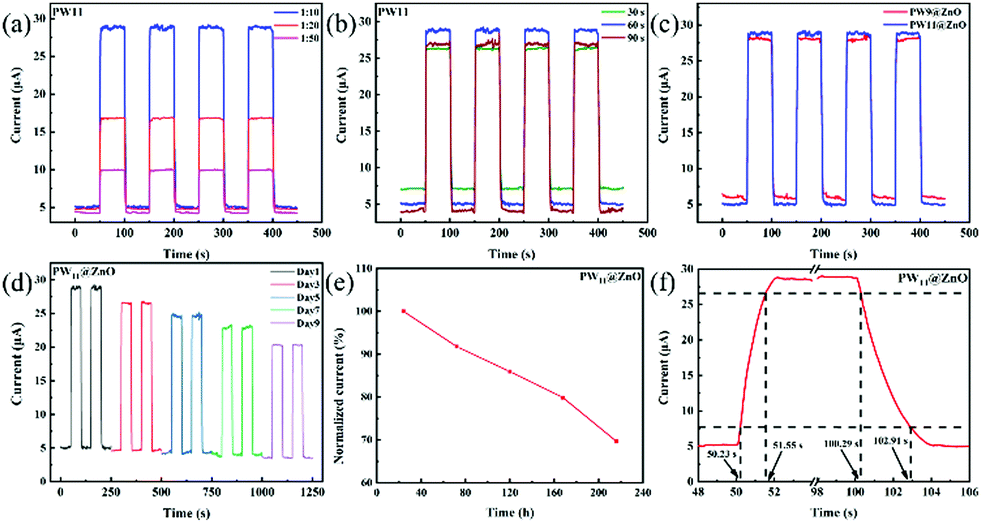 | ||
| Fig. 7 (a) The I–t curve of the photodetector when the mass doping ratios of PW11 are 1:10, 1:20 and 1:50 (spinning time 1 min). (b) The I–t curve of the photodetector at the electrospinning times of 30 s, 60 s and 90 s (the mass doping ratio of PW11 is 1:10). (c) Comparison of the optimal photodetector performance between PW9@ZnO and PW11@ZnO. (d) The stability I–t curve of the optimal photodetector modified by PW11. (e) The time curve of the highest current of the photodetector modified by PW11. (f) The rise/decay time of the optimal photodetector modified by PW11. | ||
As shown in Fig. 7b, under the optimal doping ratio of PW11, the performance of the device was tested by controlling the spinning time. It can be seen from the figure that as the spinning time increases, the dark current decreases. This phenomenon can be attributed to the increase in the thickness of the NW layer and the increase in the internal resistance as the spinning time increases. The dark current of the device is reduced. In addition, with the extension of the electrospinning time, the photocurrent showed an increasing trend first and then decreased. This phenomenon can be attributed to the increase in the number of NWs with the extension of the electrospinning time. Under light conditions, the increase of photogenerated carriers increases the photocurrent. But similar to the dark current, as the internal resistance increases further, the photocurrent begins to decrease. Therefore, the performance of the device is best when the rotation time is 60 s. Fig. 7c shows the performance comparison chart of the optimal device modified by PW9 (quality doping ratio is 1:10, spinning time 60 s) and the optimal device modified by PW11. It can be seen from the figure that the performance of the PW11 modified device is better than that of PW9. As shown in Fig. 6f, we tested the energy level band gaps of pure ZnO NWs and POMs@ZnO NWs, respectively. Among them, PW11@ZnO NWs have energy levels and band gaps that are more matched with pure ZnO NWs, so they exhibit the best photodetection performance.
Fig. 7d and e show the stability test of the PD modified by PW11, and the test interval is 48 h. It can be seen from the figure that as time increases, after 216 h, the device maintains 70% performance. The main reason for this decrease in stability can be attributed to the poor chemical stability of the POMs selected in this work in the air as traditional semiconductor materials, and will slowly decompose in the air, which will cause the performance of the device to decrease over time. Fig. 7f shows part of the I–t curve of the optimal device modified by PW11. The time required for the current to increase from 10% of the peak value to 90% (and vice versa) is defined as the rise time and the decay time, respectively. It can be seen from the figure that the rise/decay time is 1.32 s/2.62 s. Under light conditions, the average photocurrent is stable at 28.81 μA, and under no light conditions, the dark current is stable at 5.05 μA, the light–dark current difference (ΔI) reaches 23.76 μA, and the on–off ratio is 5.7. Since the chemical stability of POMs in the air is not as good as that of traditional semiconductor materials, it is easy to generate a certain dark current and reduce the on/off ratio.
The test data of PW9 and PW12 modified PDs are shown in Fig. S15 and S16 (ESI†). The doping ratios of PW9 are 1:10 and 1:20. When the doping ratio is 1:50, its photoelectric response is very weak. Moreover, after continuing to increase the doping ratio of PW9, the precursor solution becomes too viscous to electrospin. Therefore, the optimal ratio is also 1:10. Since PW12 is a saturated Keggin-type POMs it has fewer active sites than PW9 and PW11, so the performance of the device is not greatly improved, and its light response speed has also become very slow. The photoelectric response of the device is very weak when PW12 is doped into the precursor at ratios of 1:50 and 1:20. When PW12 was mixed into the precursor at a ratio of 1:15, floccules were formed in the precursor solution at the beginning, and the floccules were dissolved after continuous stirring. After continuing to increase the doping ratio, the floccules appearing cannot dissolve after continuous stirring. Therefore, the optimal doping ratio is 1:15.
As shown in Fig. 8a, this work tested the I–t curves of the photodetectors prepared by PW11@ZnO NWs at different light intensities, and the light intensities were 60, 80, 100, 120 and 140 mW cm−2. The responsivity of the device at different light intensities is calculated using the following formula:
| R = IP − Id/Plight × S | (5) |
 | (6) |
 | ||
| Fig. 8 (a) The I–t curve at different light intensities. (b) The responsivity and photocurrent at different light intensities. (c) Detection rate (D*) at different light intensities. (d) The responsivity at different wavelengths. | ||
4. Conclusions
In summary, we successfully modified the ZnO NWs with Keggin-type POMs, and made the modified ZnO NWs exhibit p-type semiconductor characteristics. Next, a series of characterization methods are used to prove the existence of POMs in the whole structure. Additionally, by controlling the electrodes of the collecting device during electrospinning, we constructed two vertical NW arrays and formed p–n homojunctions in the two layers to achieve the purpose of photodetection. The made PD has good transparency in the visible light region. Under unbiased voltage and standard AM1.5 illumination, the light–dark current difference (ΔI) can reach 23.76 μA, and its rise/decay time can reach 1.32 s/2.62 s. It is worth noting that the on/off ratio of the PD is only 5.7. Compared with other ZnO-based PDs, its good responsivity and unbiased working conditions can better adapt to possible needs. Furthermore, its preparation method is simple, which has more advantages in practical applications that may be put into use in the future. In addition, we provide new ideas for the study of photodetectors modified by polyoxometalates. There are many types of POMs that have semiconductor-like properties and diverse anionic structures. The application in the field of photodetection should not stop there.Conflicts of interest
The authors declare no competing interests.Acknowledgements
This work was financially supported by the National Natural Science Foundation of China (No. 21871041), the Natural Science Foundation of Jilin Province (No. 20180101298JC), the Technology Foundation for Selected Overseas Chinese Scholars of Personnel Ministry of China, the Science and Technology Research Project of the Education Department of Jilin Province, the Science and Technology Activities Project Preferential Funding for Selected Overseas Chinese Scholars of Jilin Province Human Resources and Social Bureau.References
- J. Han, M. He, M. Yang, Q. Han, F. Wang and F. Zhong, et al., Light-modulated vertical heterojunction phototransistors with distinct logical photocurrents, Light: Sci. Appl., 2020, 9, 167 CrossRef CAS.
- C. Li, H. Wang, F. Wang, T. Li, M. Xu and H. Wang, et al., Ultrafast and broadband photodetectors based on a perovskite/organic bulk heterojunction for large-dynamic-range imaging, Light: Sci. Appl., 2020, 9, 31 CrossRef CAS.
- D. Wang, A. E. L. Allcca, T. F. Chung, A. V. Kildishev, Y. P. Chen and A. Boltasseva, et al., Enhancing the graphene photocurrent using surface plasmons and a p-n junction, Light: Sci. Appl., 2020, 9, 126 CrossRef CAS.
- A. Aiello, Y. Wu, Z. Mi and P. Bhattacharya, Deep ultraviolet monolayer GaN/AlN disk-in-nanowire array photodiode on silicon, Appl. Phys. Lett., 2020, 116, 061104 CrossRef CAS.
- J. Zhou, Y. Gu, Y. Hu, W. Mai, P.-H. Yeh and G. Bao, et al., Gigantic enhancement in response and reset time of ZnO UV nanosensor by utilizing Schottky contact and surface functionalization, Appl. Phys. Lett., 2009, 94, 191103 CrossRef.
- B. H. Kind, H. Yan, B. Messer, M. Law and P. Yang, Nanowire Ultraviolet Photodetectors and Optical Switches, Adv. Mater., 2002, 14, 158–160 CrossRef.
- N. Nasiri, R. Bo, F. Wang, L. Fu and A. Tricoli, Ultraporous Electron-Depleted ZnO Nanoparticle Networks for Highly Sensitive Portable Visible-Blind UV Photodetectors, Adv. Mater., 2015, 27, 4336–4343 CrossRef CAS.
- W. Tian, T. Zhai, C. Zhang, S. L. Li, X. Wang and F. Liu, et al., Low-cost fully transparent ultraviolet photodetectors based on electrospun ZnO-SnO2 heterojunction nanofibers, Adv. Mater., 2013, 25, 4625–4630 CrossRef CAS PubMed.
- P. Wan, M. Jiang, T. Xu, Y. Liu and C. Kan, High-mobility induced high-performance self-powered ultraviolet photodetector based on single ZnO microwire/PEDOT:PSS heterojunction via slight ga-doping, J. Mater. Sci. Technol., 2021, 93, 33–40 CrossRef.
- X. Liu, L. Gu, Q. Zhang, J. Wu, Y. Long and Z. Fan, All-printable band-edge modulated ZnO nanowire photodetectors with ultra-high detectivity, Nat. Commun., 2014, 5, 4007 CrossRef CAS.
- Z. Li, Z. Li, Z. Shi and X. Fang, Facet-Dependent, Fast Response, and Broadband Photodetector Based on Highly Stable All-Inorganic CsCu2I3 Single Crystal with 1D Electronic Structure., Adv. Funct. Mater., 2020, 30, 2002634 CrossRef CAS.
- A. K. Rana, J. T. Park, J. Kim and C.-P. Wong, See-through metal oxide frameworks for transparent photovoltaics and broadband photodetectors, Nano Energy, 2019, 64, 103952 CrossRef CAS.
- J. Dai, C. Xu, X. Xu, J. Guo, J. Li and G. Zhu, et al., Single ZnO microrod ultraviolet photodetector with high photocurrent gain, ACS Appl. Mater. Interfaces, 2013, 5, 9344–9348 CrossRef CAS PubMed.
- H. Wang, H. Chen, L. Li, Y. Wang, L. Su and W. Bian, et al., High Responsivity and High Rejection Ratio of Self-Powered Solar-Blind Ultraviolet Photodetector Based on PEDOT:PSS/beta-Ga2O3 Organic/Inorganic p-n Junction, J. Phys. Chem. Lett., 2019, 10, 6850–6856 CrossRef CAS PubMed.
- L. Chen, C. Yang and C. Yan, High-performance UV detectors based on 2D CVD bismuth oxybromide single-crystal nanosheets, J. Mater. Sci. Technol., 2020, 48, 100–104 CrossRef.
- Y. Wang, L. Li, H. Wang, L. Su, H. Chen and W. Bian, et al., An ultrahigh responsivity self-powered solar-blind photodetector based on a centimeter-sized beta-Ga2O3/polyaniline heterojunction, Nanoscale, 2020, 12, 1406–1413 RSC.
- B. Zhao, F. Wang, H. Chen, L. Zheng, L. Su and D. Zhao, et al., An Ultrahigh Responsivity (9.7 mA W-1) Self-Powered Solar-Blind Photodetector Based on Individual ZnO–Ga2O3 Heterostructures., Adv. Funct. Mater., 2017, 27, 1700264 CrossRef.
- Z. Li, M. K. Joshi, J. Chen, Z. Zhang, Z. Li and X. Fang, Mechanically Compatible UV Photodetectors Based on Electrospun Free-Standing Y3+-Doped TiO2 Nanofibrous Membranes with Enhanced Flexibility, Adv. Funct. Mater., 2020, 30, 2005291 CrossRef CAS.
- K. Hu, F. Teng, L. Zheng, P. Yu, Z. Zhang and H. Chen, et al., Binary response Se/ZnO p-n heterojunction UV photodetector with high on/off ratio and fast speed, Laser Photonics Rev., 2017, 11, 1600257 CrossRef.
- S. Dhar, T. Majumder and S. P. Mondal, Graphene Quantum Dot-Sensitized ZnO Nanorod/Polymer Schottky Junction UV Detector with Superior External Quantum Efficiency, Detectivity, and Responsivity, ACS Appl. Mater. Interfaces, 2016, 8, 31822–31831 CrossRef CAS.
- F. Teng, L. Zheng, K. Hu, H. Chen, Y. Li and Z. Zhang, et al., A surface oxide thin layer of copper nanowires enhanced the UV selective response of a ZnO film photodetector, J. Mater. Chem. C, 2016, 4, 8416–8421 RSC.
- Y. Tu, S. Chen, X. Li, J. Gorbaciova, W. P. Gillin and S. Krause, et al., Control of oxygen vacancies in ZnO nanorods by annealing and their influence on ZnO/PEDOT:PSS diode behaviour, J. Mater. Chem. C, 2018, 6, 1815–1821 RSC.
- C. Soci, A. Zhang, B. Xiang, S. A. Dayeh, D. P. R. Aplin and J. Park, et al., ZnO Nanowire UV Photodetectors with High Internal Gain, Nano Lett., 2007, 7, 1003–1009 CrossRef CAS PubMed.
- M. Zheng, F. Yang, J. Guo, L. Zhao, X. Jiang and G. Gu, et al., Cd(OH)2@ZnO nanowires thin-film transistor and UV photodetector with a floating ionic gate tuned by a triboelectric nanogenerator., Nano Energy, 2020, 73, 104808 CrossRef CAS.
- A. K. Rana, M. Kumar, D. K. Ban, C. P. Wong, J. Yi and J. Kim, Enhancement in Performance of Transparent p-NiO/n-ZnO Heterojunction Ultrafast Self-Powered Photodetector via Pyro-Phototronic Effect., Adv. Electron. Mater., 2019, 5, 1900438 CrossRef.
- A. Bera and D. Basak, Photoluminescence and photoconductivity of ZnS-coated ZnO nanowires, ACS Appl. Mater. Interfaces, 2010, 2, 408–412 CrossRef CAS PubMed.
- Z. Zhang, Y. Ning and X. Fang, From nanofibers to ordered ZnO/NiO heterojunction arrays for self-powered and transparent UV photodetectors, J. Mater. Chem. C, 2019, 7, 223–229 RSC.
- Y. Xiang, Q. Zhou, Z. Li, Z. Cui, X. Liu and Y. Liang, et al., A Z-scheme heterojunction of ZnO/CDots/C3N4 for strengthened photoresponsive bacteria-killing and acceleration of wound healing., J. Mater. Sci. Technol., 2020, 57, 1–11 CrossRef.
- B. Deka Boruah, S. Naidu Majji, S. Nandi and A. Misra, Doping controlled pyro-phototronic effect in self-powered zinc oxide photodetector for enhancement of photoresponse, Nanoscale, 2018, 10, 3451–3459 RSC.
- G. D. Yuan, W. J. Zhang, J. S. Jie, X. Fan, J. X. Tang and I. Shafiq, et al., Tunable n-Type Conductivity and Transport Properties of Ga-doped ZnO Nanowire Arrays, Adv. Mater., 2008, 20, 168–173 CrossRef CAS.
- Y. Ning, Z. Zhang and F. Teng, X. Fang. Novel Transparent and Self-Powered UV Photodetector Based on Crossed ZnO Nanofiber Array Homojunction, Small, 2018, 14, 1703754 CrossRef.
- C. L. Hsu, Y. D. Gao, Y. S. Chen and T. J. Hsueh, Vertical p-type Cu-doped ZnO/n-type ZnO homojunction nanowire-based ultraviolet photodetector by the furnace system with hotwire assistance, ACS Appl. Mater. Interfaces, 2014, 6, 4277–4285 CrossRef CAS.
- X. Zhu, Q. Xie, H. Tian, M. Zhang, Z. Gou and S. He, et al., High photoresponse sensitivity of lithium-doped ZnO (LZO) thin films for weak ultraviolet signal photodetector, J. Alloys Compd., 2019, 805, 309–317 CrossRef CAS.
- W. Ko, S. Lee, N. Myoung and J. Hong, Solution processed vertically stacked ZnO sheet-like nanorod p–n homojunctions and their application as UV photodetectors, J. Mater. Chem. C, 2016, 4, 142–149 RSC.
- J. Lu, C. Xu, J. Dai, J. Li, Y. Wang and Y. Lin, et al., Improved UV photoresponse of ZnO nanorod arrays by resonant coupling with surface plasmons of Al nanoparticles, Nanoscale, 2015, 7, 3396–3403 RSC.
- G. C. Park, S. M. Hwang, J. H. Lim and J. Joo, Growth behavior and electrical performance of Ga-doped ZnO nanorod/p-Si heterojunction diodes prepared using a hydrothermal method, Nanoscale, 2014, 6, 1840–1847 RSC.
- W. Dai, X. Pan, S. Chen, C. Chen, W. Chen and H. Zhang, et al., ZnO homojunction UV photodetector based on solution-grown Sb-doped p-type ZnO nanorods and pure n-type ZnO nanorods, RSC Adv., 2015, 5, 6311–6314 RSC.
- O. Lupan, V. Cretu, V. Postica, M. Ahmadi, B. R. Cuenya and L. Chow, et al., Silver-doped zinc oxide single nanowire multifunctional nanosensor with a significant enhancement in response, Sens. Actuators, B, 2016, 223, 893–903 CrossRef CAS.
- H. Zhou, L. Yang, P. Gui, C. R. Grice, Z. Song and H. Wang, et al., Ga-doped ZnO nanorod scaffold for high-performance, hole-transport-layer-free, self-powered CH3NH3PbI3 perovskite photodetectors, Sol. Energy Mater. Sol. Cells, 2019, 193, 246–252 CrossRef CAS.
- T. H. Flemban, V. Singaravelu, A. A. Sasikala Devi and I. S. Roqan, Homogeneous vertical ZnO nanorod arrays with high conductivity on an in situ Gd nanolayer, RSC Adv., 2015, 5, 94670–94678 RSC.
- Y. R. Wang, Q. Huang, C. T. He, Y. Chen, J. Liu and F. C. Shen, et al., Oriented electron transmission in polyoxometalate-metalloporphyrin organic framework for highly selective electroreduction of CO2, Nat. Commun., 2018, 9, 4466 CrossRef PubMed.
- J. Lin, N. Li, S. Yang, M. Jia, J. Liu and X. M. Li, et al., Self-Assembly of Giant Mo240 Hollow Opening Dodecahedra, J. Am. Chem. Soc., 2020, 142, 13982–13988 CrossRef CAS PubMed.
- L. Chen, W. L. Chen, X. L. Wang, Y. G. Li, Z. M. Su and E. B. Wang, Polyoxometalates in dye-sensitized solar cells, Chem. Soc. Rev., 2019, 48, 260–284 RSC.
- S. Zhang, N. Liu, H. Wang, Q. Lu, W. Shi and X. Wang, Sub-Nanometer Nanobelts Based on Titanium Dioxide/Zirconium Dioxide-Polyoxometalate Heterostructures, Adv. Mater., 2021, 33, e2100576 CrossRef PubMed.
- M. Lu, M. Zhang, C. G. Liu, J. Liu, L. J. Shang and M. Wang, et al., Stable Dioxin-Linked Metallophthalocyanine Covalent Organic Frameworks (COFs) as Photo-Coupled Electrocatalysts for CO2 Reduction, Angew. Chem., Int. Ed., 2021, 60, 4864–4871 CrossRef CAS.
- L. Z. Dong, L. Zhang, J. Liu, Q. Huang, M. Lu and W. X. Ji, et al., Stable Heterometallic Cluster-Based Organic Framework Catalysts for Artificial Photosynthesis, Angew. Chem., Int. Ed., 2020, 59, 2659–2663 CrossRef CAS PubMed.
- Q. Liu, H. Yu, Q. Zhang and D. Wang, X. Wang. Temperature-Responsive Self-Assembly of Single Polyoxometalates Clusters Driven by Hydrogen Bonds., Adv. Funct. Mater., 2021, 31, 2103561 CrossRef CAS.
- G. Yang, X. Xie, M. Cheng, X. Gao, X. Lin and K. Li, et al., H4SiW12O40-catalyzed cyclization of epoxides/aldehydes and sulfonyl hydrazides: An efficient synthesis of 3,4-disubstituted 1H-pyrazoles., Chin. Chem. Lett., 2021 DOI:10.1016/j.cclet.2021.08.037.
- G. Yang, K. Li, X. Lin, Y. Li, C. Cui and S. Li, et al., Regio- and Stereoselective Synthesis of (Z)-3-Ylidenephthalides via H3PMo12O40-Catalyzed Cyclization of 2-Acylbenzoic Acids with Benzylic Alcohols, Chin. J. Chem., 2021, 39, 3017–3022 CrossRef CAS.
- G.-P. Yang, X. Zhang, Y. Liu, D. Zhang, K. Li and C. Hu, Self-assembly of Keggin-type U(VI)-containing tungstophosphates with a sandwich structure: an efficient catalyst for the synthesis of sulfonyl pyrazoles, Inorg. Chem. Front., 2021, 8, 4650–4656 RSC.
- T. Wang, T. Ji, W. Chen, X. Li, W. Guan and Y. Geng, et al., Polyoxometalate film simultaneously converts multiple low-value all-weather environmental energy to electricity, Nano Energy, 2020, 68, 104349 CrossRef CAS.
- T. Wang, M. Xu, C. Ma, Y. Gu, W. Chen and Y. Li, et al., Strategic Design of a Bifunctional NiFeCoW@NC Hybrid to Replace the Noble Platinum for Dye-Sensitized Solar Cells and Hydrogen Evolution Reactions, ACS Appl. Mater. Interfaces, 2021, 13, 25010–25023 CrossRef CAS PubMed.
- T. Wang, M. Xu, F. Li, Y. Li and W. Chen, Multimetal-based nitrogen doped carbon nanotubes bifunctional electrocatalysts for triiodide reduction and water-splitting synthesized from polyoxometalate- intercalated layered double hydroxide pyrolysis strategy, Appl. Catal., B, 2021, 280, 119421 CrossRef CAS.
- L. Chen, W. Chen, H. Tan, J. Li, X. Sang and E. Wang, The improved efficiency of quantum-dot-sensitized solar cells with a wide spectrum and pure inorganic donor–acceptor type polyoxometalate as a collaborative cosensitizer, J. Mater. Chem. A, 2016, 4, 4125–4133 RSC.
- X. Xu, L. Zhang, T. Wang, Y. Li, T. Ji and W. Chen, et al., The dual effect of “inorganic fullerene” {Mo132} doped with SnO2 for efficient perovskite-based photodetectors, Mater. Chem. Front., 2021, 5, 6931–6940 RSC.
- X. Xu, M. Xie, K. Xu and Y. Zhao, g-C3N4@PMo12 composite material double adjustment improves the performance of perovskite-based photovoltaic devices, Sol. Energy, 2020, 209, 363–370 CrossRef CAS.
- S. Yang, H. Ma, Y. Luo and J. Gong, Photocurrent Response of Surface-Functionalized Metal Oxides with Well-Matched Energy Levels: From Nothing to Something, ChemPhysChem, 2012, 13, 2289–2292 CrossRef CAS PubMed.
- H. Wang, L. Fang, Y. Yang, R. Hu and Y. Wang, Immobilization Na7PW11O39 on quanternary ammonium functionalized chloromethylated polystyrene by electrostatic interactions: An efficient recyclable catalyst for alcohol oxidation, Appl. Catal., A, 2016, 520, 35–43 CrossRef CAS.
- W. H. Fang, W. D. Wang and G. Y. Yang, A novel poly(polyoxometalate) built by {Cu9}/{Cu5} clusters and {PW9}/{PW10}/{PW11} lacunary fragments, Dalton Trans., 2015, 44, 12546–12549 RSC.
- H. Shi, T. Zhao, J. Wang, Y. Wang, Z. Chen and B. Liu, et al., Fabrication of g-C3N4/PW12/TiO2 composite with significantly enhanced photocatalytic performance under visible light., J. Alloys Compd., 2021, 860, 157924 CrossRef CAS.
- L. D'Souza, M. Noeske, R. M. Richards and U. Kortz, Polyoxotungstate stabilized palladium, gold, and silver nanoclusters: a study of cluster stability, catalysis, and effects of the stabilizing anions, J. Colloid Interface Sci., 2013, 394, 157–165 CrossRef PubMed.
- Q. Zhang, T. Wang, Z. Sun, L. Xi and L. Xu, Performance improvement of photoelectrochemical NO2 gas sensing at room temperature by BiVO4-polyoxometalate nanocomposite photoanode, Sens. Actuators, B, 2018, 272, 289–295 CrossRef CAS.
- W. Liu, F. Zhu, B. Ge, L. Sun, Y. Liu and W. Shi, MOF derived ZnO/C@(Ni,Co)Se2 core–shell nanostructure on carbon cloth for high-performance supercapacitors, Chem. Eng. J., 2022, 427, 130788 CrossRef CAS.
- H. B. Lee, R. T. Ginting, S. T. Tan, C. H. Tan, A. Alshanableh and H. F. Oleiwi, et al., Controlled Defects of Fluorine-incorporated ZnO Nanorods for Photovoltaic Enhancement, Sci. Rep., 2016, 6, 32645 CrossRef CAS.
- H. B. Lee, N. Kumar, M. M. Ovhal, Y. J. Kim, Y. M. Song and J. W. Kang, Dopant-Free, Amorphous–Crystalline Heterophase SnO2 Electron Transport Bilayer Enables >20% Efficiency in Triple-Cation Perovskite Solar Cells, Adv. Funct. Mater., 2020, 30, 2001559 CrossRef CAS.
- X. Wang, Q. Di, X. Wang, H. Zhao, B. Liang and J. Yang, Effect of oxygen vacancies on photoluminescence and electrical properties of (200) oriented fluorine-doped SnO2 films., Mater. Sci. Eng., B, 2019, 250, 114433 CrossRef CAS.
- A. Allagui, H. Alawadhi, M. Alkaaby, M. Gaidi, K. Mostafa and Y. Abdulaziz, Mott-Schottky analysis of flower-like ZnO microstructures with constant phase element behavior, Phys. Status Solidi A, 2016, 213, 139–145 CrossRef CAS.
- F. R. Li, T. Wang, Y. J. Li, X. Y. Xu, C. H. Ma and W. L. Chen, et al., Heteropoly Blue/Protonation-Defective Graphitic Carbon Nitride Heterojunction for the Photo-Driven Nitrogen Reduction Reaction, Inorg. Chem., 2021, 60, 5829–5839 CrossRef CAS PubMed.
Footnote |
| † Electronic supplementary information (ESI) available. See DOI: 10.1039/d1qm01246k |
| This journal is © the Partner Organisations 2022 |