
Decoupling of CVD-grown epitaxial graphene using NaCl intercalation†
Yohan
Kim
a,
Huijun
Han
a,
Da
Luo
 b,
Rodney S.
Ruoff
bcad and
Hyung-Joon
Shin
*ab
b,
Rodney S.
Ruoff
bcad and
Hyung-Joon
Shin
*ab
aDepartment of Materials Science and Engineering, Ulsan National Institute of Science and Technology (UNIST), Ulsan 44919, Republic of Korea. E-mail: shinhj@unist.ac.kr
bCenter for Multidimensional Carbon Materials (CMCM), Institute for Basic Science (IBS), Ulsan 44919, Republic of Korea
cDepartment of Chemistry, Ulsan National Institute of Science and Technology (UNIST), Ulsan 44919, Republic of Korea
dSchool of Energy and Chemical Engineering, Ulsan National Institute of Science and Technology (UNIST), Ulsan 44919, Republic of Korea
First published on 3rd November 2022
Abstract
The structural and electronic properties of graphene grown on catalytic metal surfaces are significantly modified via graphene-substrate interaction. To minimize the influence of the metal substrate, a dielectric buffer layer can be introduced between the graphene and metal substrate. However, the catalytic synthesis of graphene limits the potential alternatives for buffer layers. The intercalation of atoms below the graphene layer is a promising method that does not require the chemical treatment of graphene or the substrate. In this study, the electronic and structural properties of single-layer graphene (SLG) on the Cu(111) substrate intercalated with ultrathin NaCl thin films were investigated using scanning tunnelling microscopy. The intercalation of the NaCl monolayer decoupled SLG from the metal substrate, thereby producing quasi-freestanding graphene.
Introduction
Graphene has attracted considerable interest owing to its unique electronic and optical properties.1 The chemical vapor deposition (CVD) growth on transition metal substrates is a promising method for growing high-quality large-area graphene films.2 The metal substrate acts as a catalyst that converts hydrocarbon species into graphene. However, the strong interaction between graphene and the substrate alters the intrinsic properties of graphene. For example, charge transfer changes the work function of graphene, and the scattering of the charge carrier reduces the high-quality transport properties of graphene.3,4 Additionally, a structural corrugation is observed, which indicates an increase in strain within the graphene layer.5 In order to minimize the effect of the substrate and for certain applications, graphene is transferred onto insulating substrates, such as hexagonal boron nitride (h-BN).6,7 However, it is difficult to avoid corrugation or contamination during the transfer process. The direct growth of graphene has been demonstrated on insulating substrates.8–10 However, the limitations of low growth rate and small grain size persists.9 Recently, Li et al. reported the preparation of a single-layer graphene (SLG) on the electrically insulating sapphire wafer.10 After growing graphene at the interface between sapphire and Cu film, the Cu layer was peeled off from the surface of graphene.Introducing foreign atoms between graphene and the metal substrate via intercalation is an alternative method used to decouple graphene from the substrate.11,12 Several intercalants, such as B, O, Si, Pb, In, Au, and Ce, have been used for the separation of epitaxial graphene and metal substrates at the nanoscale level.13–18 These intercalants decouple graphene from the substrate, which can be observed by the suppressed surface state of the substrate. However, most intercalants still alter the properties of graphene. For example, boron-intercalated-graphene is modified to possess a threefold linear feature by the underlying borophene sheets, and the intercalated Si or Ce induces moiré superlattice in graphene. Alkali metal and Pb intercalations lead to the doping of graphene through charge transfer.4,19 Therefore, intercalants with strong decoupling effects are required to develop freestanding graphene. Previous studies have demonstrated that “quasi-freestanding graphene” does not exhibit an additional superstructure, except the graphene honeycomb lattice.5,14,20
In this study, the intercalation of NaCl at the interface between SLG and Cu(111) was investigated using scanning tunnelling microscopy (STM) and scanning tunnelling spectroscopy (STS). A clean graphene surface was ensured before the NaCl films were deposited on the SLG/Cu(111). NaCl was diffused between the graphene and Cu substrate after annealing at 600 K. The intercalated region was higher than the SLG/Cu region, and the specific features in the topography originating from the Cu substrate disappeared. The STS results exhibited a higher local density of state (LDOS), work function, and dielectric constant compared to those of SLG/Cu(111). These observations demonstrated the structural and electronic decoupling of graphene from the Cu substrate, due to the intercalation of a NaCl film between graphene and Cu(111). As a result, the NaCl-intercalated graphene behaved as freestanding graphene.
Methods
A large-area continuous single-crystal SLG film was grown using the CVD method on a single crystalline Cu(111) foil, which was prepared via the contact-free annealing method.21,22 Once SLG film covered the whole surface of Cu(111), we couldn't find any oxide layer at the interface.23 The SLG/Cu(111) sample was transferred from ambient to ultrahigh vacuum (UHV) STM chamber, followed by annealing at 800 K. The NaCl films were deposited by thermal evaporation. When the substrate was maintained at room temperature (RT) during deposition, NaCl islands of two-monolayer (ML) thickness were formed. The intercalation of NaCl islands was achieved by annealing the sample at 600 K. The STM experiments were performed using a low-temperature STM. The sample temperature and base pressure were 1.1 K and 4.0 × 10⁻¹¹ Torr, respectively. The dI/dV and dz/dV spectra were measured using a lock-in technique with a bias voltage modulation of 50 mV at 727 Hz.Results and discussion
Fig. 1(a) shows the SLG grown on a single crystalline Cu(111) foil using the CVD method. In the STM topography, the Cu vacancy-induced Kekulé distortion is observed on the graphene. Kekulé distortion is originated in the long-range electronic interaction between Cu vacancies and SLG.24 The Kekulé order manifests with a larger honeycomb pattern with a darker depression, and it exhibited a R30° supercell (labelled as R3, a red diamond) in addition to the graphene unit cell (a blue diamond). The magnified STM image clearly shows the Kekulé-ordered structure in SLG (Fig. S1a†). The Cu vacancies underneath the graphene appeared as bright dots in STM topography, which had a uniform height of ∼80 pm (Fig. S1b†). A large-area topography revealed a spiral pattern, which was a reconstruction of the underlying Cu(111) surface and vacancies near the node of the spiral [bottom in Fig. 1(a)]. The spirals and Kekulé distortion were structural variations that originated from the Cu substrate. The thermal evaporation of NaCl on an SLG/Cu(111) sample formed rectangular NaCl islands [Fig. 1(b)]. Although the lattice mismatch between NaCl(001) and graphene was over 10%, the majority of the NaCl islands grew with specific orientation, which indicated commensurate growth. Due to a higher DOS at Cl− than Na+,25 Cl anions were imaged as protrusions in the STM topography, which formed a square unit cell in the atomically resolved image [bottom in Fig. 1(b)].26 The straight step edges were formed along the nonpolar directions of NaCl islands. The Fourier transform (FT) of the SLG/Cu(111) topography exhibited two distinct sets of periodicities in the SLG/Cu(111) system [left in Fig. 1(c)]. The outer six spots corresponded to the graphene reciprocal lattice (blue circles), and the inner six spots corresponded to the Kekulé R3 super cell (red circles). After deposition of NaCl, FT of the topography [right in Fig. 1(c)] featured only four spots corresponding to Cl lattice (green circles). Even though there is a large mismatch owing to the lattice constants of NaCl and graphene, for the NaCl islands we have observed, there was no moiré pattern. Most NaCl islands were 2 ML and their apparent height varies as a function of the imaging bias (Fig. S2†). The thickness of the films (5.5 Å) measured at the sample bias above the conduction band minimum (3.6 V) was close to the theoretical value (5.76 Å) [Fig. 1(d)]. However, the apparent height measured at lower bias (inside of its band gap) was reduced to about 3.0 Å owing to its low DOS.26–30 The islands were easy to crack and move (Fig. S3†) while imaging the NaCl islands on SLG/Cu(111) with the STM tip, which indicated the weakly-physisorbed state of NaCl on the graphene surface.27,29 Although previous density functional theory (DFT) calculations predicted that SLG/NaCl/Cu(111) structure is more stable than NaCl/SLG/Cu(111),5 Palacio et al. reported that the NaCl film is desorbed from the surface of graphene without intercalation by annealing at 823 K on the graphene surface.27 In this study, the NaCl/SLG sample was annealed at 600 K for 5 h in an attempt to achieve intercalation of NaCl films under UHV. It was not easy to achieve a large-scale intercalation in the UHV system. Since the vapour pressure of NaCl was reported to be 1.4 × 10⁻⁵ Torr at 760 K,31 most NaCl films under UHV conditions evaporated rather than intercalated through SLG at this temperature. The intercalation on a large scale would likely be possible by using a heat treatment under higher pressure. In the NaCl-deposited SLG, the SLG inhibited a spontaneous intercalation of NaCl at RT. We speculate that the temperature window is very narrow for the intercalation. NaCl was diffused between SLG and Cu during annealing, which formed crystalline NaCl films between graphene and Cu.
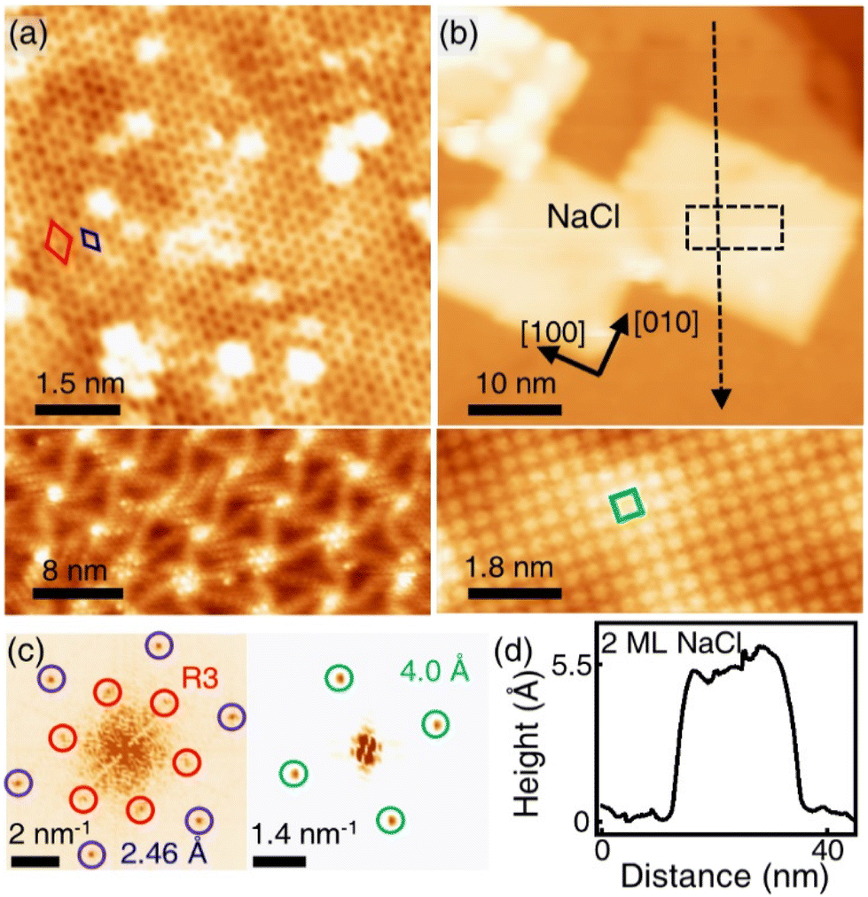 | ||
| Fig. 1 NaCl films on SLG/Cu(111). (a) STM topography images of the SLG on Cu(111). Top: atomically resolved STM topography represents the graphene honeycomb lattice (blue diamond) and R3 supercell (red diamond) (Vs = 50 mV: sample bias, It = 0.7 nA: tunnelling current); bottom: a large-area topography depicts the presence of a spiral pattern with a wavelength of 6.0 nm (Vs = 0.1 V, It = 1.0 nA). (b) Top: after NaCl deposition, (001) oriented NaCl islands cover the graphene surface (Vs = 4.0 V, It = 50 pA); bottom: zoomed-in STM image of the NaCl island indicated by the dashed rectangle in the top shows the bright Cl− ions (Vs = 3.0 V, It = 50 pA). (c) Fourier transforms of the STM images, showing graphene lattice (blue circles), R3 supercell (red circles), and Cl− ions (green circles). Left and right images are obtained from the top panel of (a) and the bottom panel of (b), respectively. (d) Height profile along the black arrow in (b). | ||
Only the bare graphene region (labelled as SLG/Cu) and the bright region which is identified as NaCl-intercalated graphene (labelled as SLG/NaCl) remained on the surface (Fig. 2a). The bright regions were oriented in the <100> directions of NaCl (Fig. S5†). The honeycomb lattice observed in the bright region confirmed the presence of graphene. The dI/dV spectrum at the region exhibited a V-shaped curve, where the Dirac point was located near zero bias, which is a hallmark of a two-dimensional (2D) Dirac material [Fig. 2(b), red curve].32,33 Compared with the relatively broad STS curve measured on SLG/Cu, the sharp V-shaped dI/dV spectrum was attributed to the suppressed electronic screening effect from the metal substrate. It demonstrated that graphene was electronically decoupled from the metal substrate after intercalation.13,18
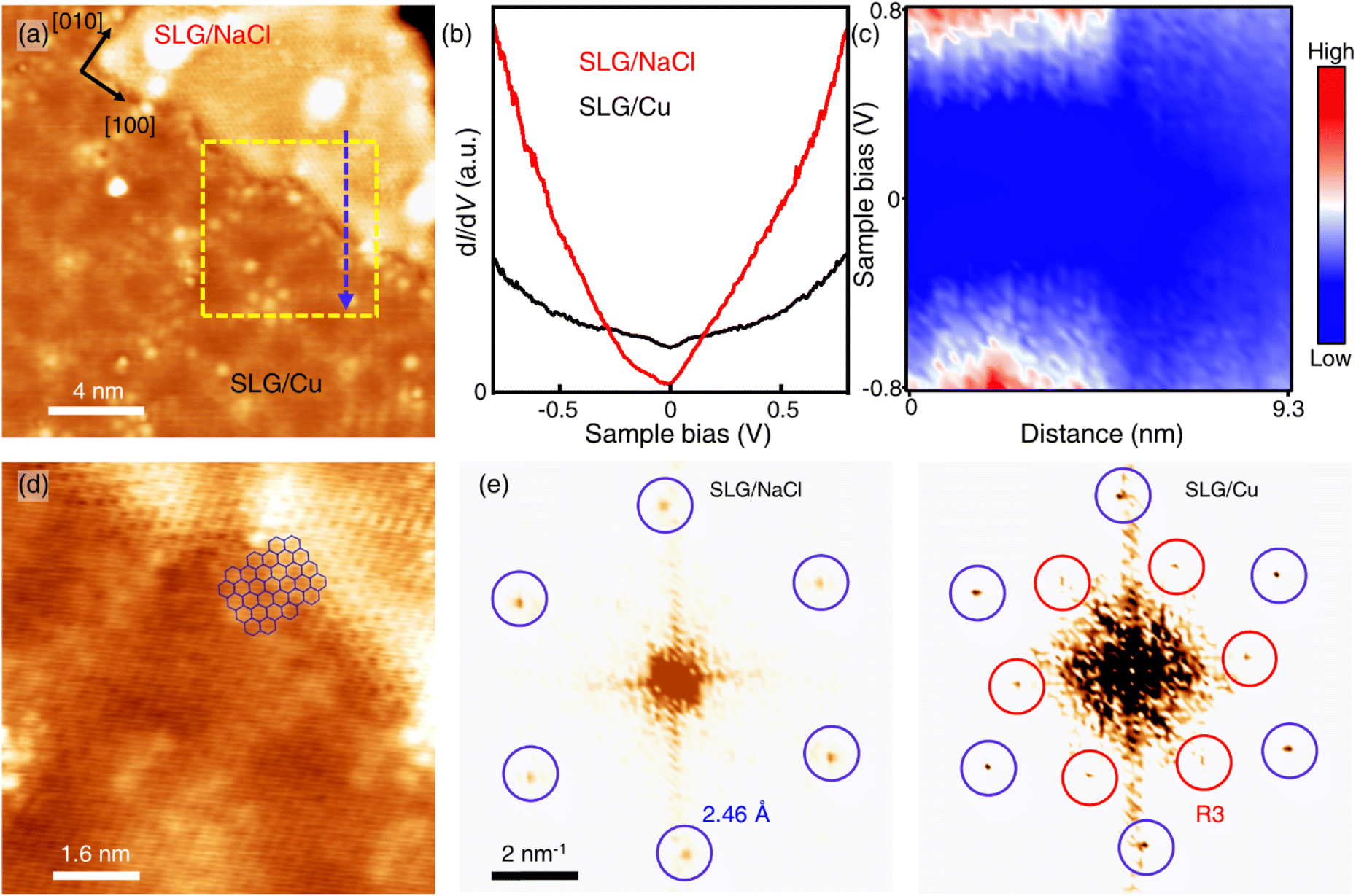 | ||
| Fig. 2 Intercalation of NaCl between SLG and Cu(111). (a) STM topography image of SLG/Cu and NaCl-intercalated graphene (Vs = −0.3 V, It = 50 pA). (b) Differential conductance (dI/dV) spectra of SLG/Cu and NaCl-intercalated graphene. (c) One-dimensional dI/dV map across the boundary of domains along the blue dashed arrow in (a). (d) Zoomed-in topography indicated by the yellow dashed square in (a) (Vs = −5 mV, It = 0.3 nA). (e) FT images obtained from SLG/NaCl (left) and SLG/Cu (right) (see Fig. S4† for topography). | ||
Fig. 2(c) depicts the one-dimensional (1D) dI/dV mapping across the SLG/Cu and SLG/NaCl boundary. A drastic electronic transition from SLG/Cu to SLG/NaCl without the evolution of an interface state is observed. Additionally, as indicated by the zoomed-in image of the SLG/Cu-SLG/NaCl boundary and FT images [Fig. 2(d) and (e)], the graphene lattice remained continuous across the boundary with the same lattice orientations. Furthermore, Cu vacancies, Kekulé distortion and moiré structure at SLG/NaCl could not be determined (Fig. S6†), which indicated that the intercalation of NaCl caused the structural decoupling from the substrate. A disappearance of the spiral pattern implies that NaCl intercalation alleviated the distortion within the SLG layer and made it flat. We can observe that the boundary is not distorted severely. The spacing between graphene and copper surface is wide enough to accommodate 1 ML NaCl film with low strain in graphene.
The local work function (LWF) of graphene can be probed by measuring field-emission resonances (FERs) because new current channels arise when the Fermi level of the STM tip exceeds the vacuum level of graphene.34 The 1D dz/dV mapping over SLG/NaCl was performed to examine the change in the LWF of the domains (Fig. 3). In the SLG/Cu region, where Kekulé distortion was found, the first peak splits into two subpeaks located at approximately 3.7 and 4.1 eV. Notably, the splitting of peak was not distant from the Kekulé distortion (Fig. S7†). The energy splitting of FER (0.4–0.5 eV) has been observed from borophane and InAs, which is attributed to the surface potential corrugation.35,36 It was not observed for high-order FERs. In the case of SLG/Cu, the local potential corrugation from the Kekulé distortion is expected to result in the splitting of peak in FER. The NaCl film electronically decouples the graphene from the Kekulé-ordered Cu vacancies. Therefore, the energy splitting of the first FER peak was not observed for the SLG/NaCl and this implies that the surface state disperses freely in the direction parallel to the surface.
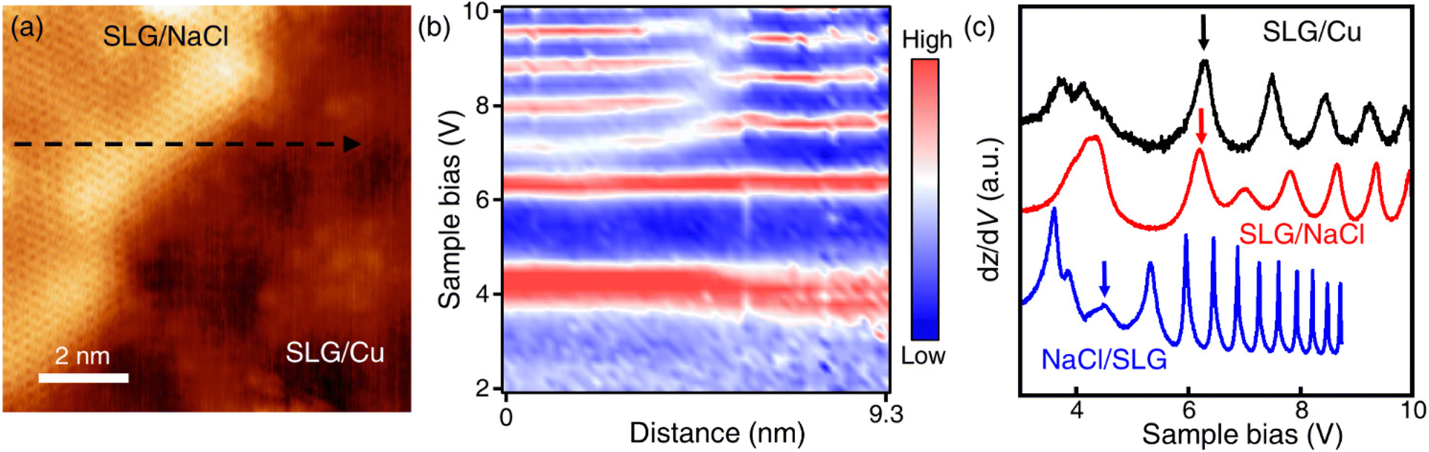 | ||
| Fig. 3 Variation in FER spectra owing to NaCl intercalation and adsorption. (a) STM topography image of SLG/Cu and NaCl-intercalated graphene (Vs = 50 mV, It = 0.4 nA). (b) 1D dz/dV map along the dashed arrow in (a). (c) FER spectra measured on the SLG/Cu (black), SLG/NaCl (red), NaCl/SLG (blue). FER peaks (n = 1) are marked by arrows in (c). | ||
The LWF (ϕ) of a combined-material system can be calculated from FERs according to the following equation:34
 | (1) |
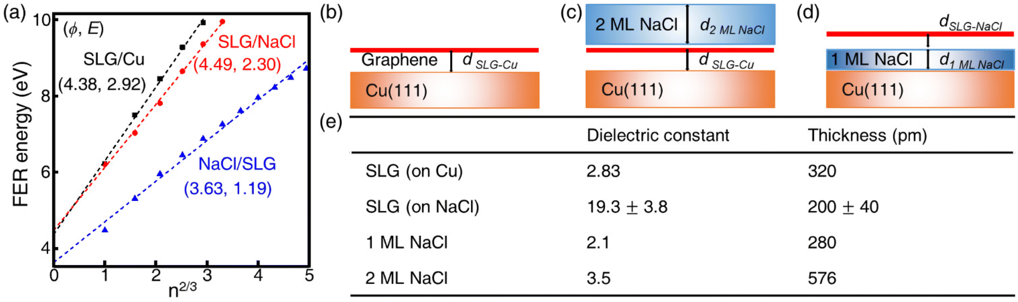 | ||
| Fig. 4 Modified work function and dielectric constant of SLG owing to NaCl intercalation and adsorption. (a) Extracted and fitted FER peak energies versus n2/3 (n ≥ 1). Black: SLG/Cu, red: SLG/NaCl, and blue: NaCl/SLG. Work function (ϕ, eV) and electric field (E, V nm−1) are obtained from the y-intercept and the slope of the plots, respectively. Structural schematics of (b) SLG/Cu, (c) NaCl/SLG, and (d) SLG/NaCl. (e) Dielectric constants and thicknesses of SLG, 1 ML NaCl, and 2 ML NaCl layers. | ||
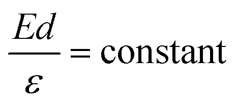
The apparent height and applied electric field were different even under the same sample bias for SLG/Cu, SLG/NaCl, and NaCl/SLG owing to the adsorption or intercalation of the dielectric NaCl layer. According to eqn (1), the electric field can be derived from the slope of the plots in Fig. 4(a). The calculated electric field strengths were 2.92, 2.30, and 1.19 V nm−1 at SLG/Cu, SLG/NaCl, and NaCl/SLG, respectively. The electric field strength was decreased by 0.62 V nm−1 through the intercalation of NaCl, while that of the 2 ML NaCl on SLG was reduced by 1.73 V nm−1. Furthermore, the dielectric constant, ε, of the layer was estimated using a simple parallel capacitor model [Fig. 4(b)–(e)]. It was assumed that the voltage drop across the thin films is constant during the FER measurements, i.e.,
The dielectric constant of the SLG on Cu(111), εSLG-Cu, was calculated to be 2.83. The value of εSLG-Cu is significantly smaller than that of freestanding graphene (ε = 15.0).41,42 When the SLG is placed on a metal substrate, the supporting substrate causes dielectric screening, which results in a decreased Fermi velocity and an enhanced electron–electron interaction in the ultrathin graphene layer.43 Therefore, the dielectric constant of the SLG became smaller due to interlayer electronic coupling between SLG and Cu.
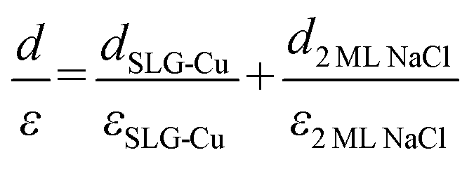
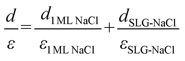
Regarding the intercalated NaCl layer of SLG/NaCl, it was expected to be a 1 ML-thick NaCl film owing to its low apparent height (40 pm). The dielectric constant of bulk NaCl is 5.9, which is reported to decrease with a decrease in the number of layers.44,45 Hence, the intercalated 1 ML NaCl would have a smaller dielectric constant than that of the adsorbed 2 ML NaCl. In the case of the SLG/NaCl, the effective thickness of the films was expressed as:
Conclusions
The decoupling of an epitaxial single crystal SLG on Cu(111) was achieved by the intercalation of 1 ML NaCl film. Annealing NaCl films adsorbed on the SLG surface led to the diffusion of NaCl to the interface between SLG and Cu to form a 1 ML NaCl film. The intercalated NaCl film decoupled SLG from the Cu substrate, and the SLG exhibited the electronic and structural properties of quasi-freestanding graphene. The intercalation of the 1 ML-thick NaCl film was quantitatively verified in terms of the work function, applied electric field, and dielectric constant. Unlike conventional techniques46–51 for transferring graphene onto insulating substrates, our method does not contaminate nor damage the graphene, which also provides a chance of tuning the physical and electrical properties of large-area graphene films grown on the various catalytic substrates. It is expected that the intercalation of ionic materials to form a vertical heterostructure to minimize the effect of substrate can be used for potential applications of various 2D materials to prepare clean and economical quasi-freestanding layers for nanoelectronics.Author contributions
Yohan Kim: conceptualization, investigation, data curation, formal analysis, and writing–original draft. Huijun Han: investigation, writing–review and editing. Da Luo: resources, writing–review and editing. Rodney S. Ruoff: resources, funding acquisition, writing–review and editing. Hyung-Joon Shin: conceptualization, supervision, funding acquisition, and writing–review and editing.Conflicts of interest
There are no conflicts to declare.Acknowledgements
This work was supported by the National Research Foundation of Korea (NRF) funded by the Ministry of Science, ICT & Future Planning (Grant No. 2021R1A2C2006219) and by IBS (IBS-R019-D1).References
- A. K. Geim and K. S. Novoselov, Nat. Mater., 2007, 6, 183–191 CrossRef CAS PubMed.
- X. Li, W. Cai, J. An, S. Kim, J. Nah, D. Yang, R. Piner, A. Velamakanni, I. Jung, E. Tutuc, S. K. Banerjee, L. Colombo and R. S. Ruoff, Science, 2009, 324, 1312 CrossRef CAS PubMed.
- S. Wundrack, D. M. Pakdehi, P. Schädlich, F. Speck, K. Pierz, T. Seyller, H. W. Schumacher, A. Bakin and R. Stosch, Phys. Rev. B, 2019, 99, 045443 CrossRef CAS.
- A. Nagashima, N. Tejima and C. Oshima, Phys. Rev. B, 1994, 50, 17487–17495 CrossRef CAS PubMed.
- M. Schulzendorf, A. Hinaut, M. Kisiel, R. Jöhr, R. Pawlak, P. Restuccia, E. Meyer, M. C. Righi and T. Glatzel, ACS Nano, 2019, 13, 5485 CrossRef CAS PubMed.
- D. Wong, J. Velasco, L. Ju, J. Lee, S. Kahn, H.-Z. Tsai, C. Germany, T. Taniguchi, K. Watanabe, A. Zettl, F. Wang and M. F. Crommie, Nat. Nanotechnol., 2015, 10, 949 CrossRef CAS PubMed.
- J. Xue, J. Sanchez-Yamagishi, D. Bulmash, P. Jacquod, A. Deshpande, K. Watanabe, T. Taniguchi, P. Jarillo-Herrero and B. J. Leroy, Nat. Mater., 2011, 10, 282–285 CrossRef CAS PubMed.
- B. G. Shin, D. H. Boo, B. Song, S. Jeon, M. Kim, S. Park, E. S. An, J. S. Kim, Y. J. Song and Y. H. Lee, ACS Nano, 2019, 13, 6662–6669 CrossRef CAS PubMed.
- S. Tang, H. Wang, H. S. Wang, Q. Sun, X. Zhang, C. Cong, H. Xie, X. Liu, X. Zhou, F. Huang, X. Chen, T. Yu, F. Ding, X. Xie and M. Jiang, Nat. Commun., 2015, 6, 6499 CrossRef CAS PubMed.
- J. Li, M. Chen, A. Samad, H. Dong, A. Ray, J. Zhang, X. Jiang, U. Schwingenschlögl, J. Domke, C. Chen, Y. Han, T. Fritz, R. S. Ruoff, B. Tian and X. Zhang, Nat. Mat., 2022, 21, 740–747 CrossRef CAS PubMed.
- N. Briggs, Z. M. Gebeyehu, A. Vera, T. Zhao, K. Wang, A. D. Duran, B. Bersch, T. Bowen, K. L. Knappenberger and J. A. Robinson, Nanoscale, 2019, 11, 15440 RSC.
- M. Petrović, I. Š. Rakić, S. Runte, C. Busse, J. T. Sadowski, P. Lazić, I. Pletikosić, Z. H. Pan, M. Milun, P. Pervan, N. Atodiresei, R. Brako, D. Šokćević, T. Valla, T. Michely and M. Kralj, Nat. Commun., 2013, 4, 2772 CrossRef PubMed.
- X. Liu and M. C. Hersam, Sci. Adv., 2019, 5, 6444 CrossRef PubMed.
- S. L. Kovalenko, B. V. Andryushechkin and K. N. Eltsov, Carbon, 2020, 164, 198 CrossRef CAS.
- A. Yurtsever, J. Onoda, T. Iimori, K. Niki, T. Miyamachi, M. Abe, S. Mizuno, S. Tanaka, F. Komori and Y. Sugimoto, Small, 2016, 12, 3956 CrossRef CAS PubMed.
- T. Hu, D. Yang, W. Hu, Q. Xia, F. Ma and K. Xu, Carbon, 2021, 171, 829 CrossRef CAS.
- L. Huang, Y. Pan, L. Pan, M. Gao, W. Xu, Y. Que, H. Zhou, Y. Wang, S. Du and H.-J. Gao, Appl. Phys. Lett., 2011, 99, 163107 CrossRef.
- L. Meng, R. Wu, H. Zhou, G. Li, Y. Zhang, L. Li, Y. Wang and H.-J. Gao, Appl. Phys. Lett., 2012, 100, 083101 CrossRef.
- A. Sandin, T. Jayasekera, J. E. Rowe, K. W. Kim, M. B. Nardelli and D. B. Dougherty, Phys. Rev. B, 2012, 85, 125410 CrossRef.
- X. Wang, H. Guo, J. Lu, H. Lu, X. Lin, C. Shen, L. Bao, S. Du and H.-J. Gao, Chin. Phys. B, 2021, 30, 048102 CrossRef CAS.
- S. Jin, M. Huang, Y. Kwon, L. Zhang, B.-W. Li, S. Oh, J. Dong, D. Luo, M. Biswal, B. V. Cunning, P. V. Bakharev, I. Moon, W. J. Yoo, D. C. Camacho-Mojica, Y.-J. Kim, S. H. Lee, B. Wang, W. K. Seong, M. Saxena, F. Ding, H.-J. Shin and R. S. Ruoff, Science, 2018, 362, 1021 CrossRef CAS PubMed.
- D. Luo, M. Wang, Y. Li, C. Kim, K. M. Yu, Y. Kim, H. Han, M. Biswal, M. Huang, Y. Kwon, M. Goo, D. C. Camacho-Mojica, H. Shi, W. J. Yoo, M. S. Altman, H.-J. Shin and R. S. Ruoff, Adv. Mater., 2019, 31, 1903615 CrossRef PubMed.
- D. Luo, X. Wang, B. Li, C. Zhu, M. Huang, L. Qiu, M. Wang, S. Jin, M. Kim, F. Ding and R. S. Rouff, Adv. Mater., 2021, 33, 2102697 CrossRef CAS PubMed.
- C. Gutiérrez, C.-J. Kim, L. Brown, T. Schiros, D. Nordlund, E. B. Lochocki, K. M. Shen, J. Park and A. N. Pasupathy, Nat. Phys., 2016, 12, 950–958 Search PubMed.
- W. Hebenstreit, J. Redinger, Z. Horozova, M. Schmid, R. Podloucky and P. Varga, Surf. Sci., 1999, 424, 321–328 CrossRef.
- C. C. Leon, A. Grewal, K. Kuhnke, K. Kern and O. Gunnarsson, Nat. Commun., 2022, 13, 981 CrossRef CAS PubMed.
- I. Palacio, K. Lauwaet, L. Vázquez, F. J. Palomares, H. González-Herrero, J. I. Martínez, L. Aballe, M. Foerster, R. García-Hernández and J. Martín-Gago, Nanoscale, 2019, 11, 16767 RSC.
- M. Imai-Imada, H. Imada, K. Miwa, J. Jung, T. K. Shimizu, M. Kawai and Y. Kim, Phys. Rev. B, 2018, 98, 201403 CrossRef CAS.
- C. Bombis, F. Ample, J. Mielke, M. Mannsberger, C. J. Villagómez, C. Roth, C. Joachim and L. Grill, Phys. Rev. Lett., 2010, 104, 185502 CrossRef PubMed.
- K. Lauwaet, K. Schouteden, E. Janssens, C. V. Haesendonck and P. Lievens, J. Phys.: Condens. Matter, 2012, 24, 475507 CrossRef PubMed.
- B. H. Zimm and J. E. Mayer, J. Chem. Phys., 1944, 12, 362 CrossRef CAS.
- B. Borca, C. Castenmiller, M. Tsvetanova, K. Sotthewes, A. N. Rudenko and H. J. W. Zandvliet, 2D Mater., 2020, 7, 035021 CrossRef CAS.
- A. Luican, G. Li and E. Y. Andrei, Solid State Commun., 2009, 149, 1151 CrossRef CAS.
- O. Y. Kolesnychenko, Y. A. Kolesnichenko, O. Shklyarevskii and H. van Kempen, Physica. B, 2000, 291, 246 CrossRef CAS.
- Q. Li, V. S. C. Kolluru, M. S. Rahn, E. Schwenker, S. Li, R. G. Hennig, P. Darancet, M. K. Y. Chan and M. C. Hersam, Science, 2021, 371, 1143 CrossRef CAS PubMed.
- J. Martínez-Blanco, S. C. Erwin, K. Kanisawa and S. Fölsch, Phys. Rev. B, 2015, 92, 115444 CrossRef.
- A. Siokou, F. Ravani, S. Karakalos, O. Frank, M. Kalbac and C. Galiotis, Appl. Surf. Sci., 2011, 257, 9785 CrossRef CAS.
- D. Niesner and T. Fauster, J. At., Mol., Condens. Matter Nano Phys., 2014, 26, 393001 CrossRef PubMed.
- G. Giovannetti, P. A. Khomyakov, G. Brocks, V. M. Karpan, J. van den Brink and P. J. Kelly, Phys. Rev. Lett., 2008, 101, 026803 CrossRef CAS PubMed.
- S. Prada, U. Martinez and G. Pacchioni, Phys. Rev. B, 2008, 78, 235423 CrossRef.
- J. P. Reed, B. Uchoa, Y. I. Joe, Y. Gan, D. Casa, E. Fradkin and P. Abbamonte, Science, 2010, 330, 805–808 CrossRef CAS PubMed.
- D. C. Elias, R. V. Gorbachev, A. S. Mayorov, S. V. Morozov, A. A. Zhukov, P. Blake, L. A. Ponomarenko, I. V. Grigorieva, K. S. Novoselov, F. Guinea and A. K. Geim, Nat. Phys., 2012, 8, 701–704 Search PubMed.
- Y. Wang, V. W. Brar, A. V. Shytov, Q. Wu, W. Regan, H.-Z. Tsai, A. Zettl, L. S. Levitov and M. F. Crommie, Nat. Phys., 2012, 8, 653 Search PubMed.
- K. Natori, D. Otani and N. Sano, Appl. Phys. Lett., 1998, 73, 632 CrossRef CAS.
- C. Andeen, J. Fontanella and D. Schuele, Phys. Rev. B: Condens. Matter Mater. Phys., 1970, 2, 5068 CrossRef.
- A. Ambrosi and M. Pumera, Nanoscale, 2014, 6, 472–476 RSC.
- Y. Wang, Y. Zheng, X. Xu, E. Dubuisson, Q. Bao, J. Lu and K. P. Loh, ACS Nano, 2011, 5, 9927–9933 CrossRef CAS PubMed.
- L. Gao, G. Ni, Y. Liu, B. Liu, A. H. C. Neto and K. P. Loh, Nature, 2014, 505, 190–194 CrossRef CAS PubMed.
- J. W. Suk, A. Kitt, C. W. Magnuson, Y. Hao, S. Ahmed, J. An, A. K. Swan, B. B. Goldberg and R. S. Ruoff, ACS Nano, 2011, 5, 6916–6924 CrossRef CAS PubMed.
- B. N. Chandrashekar, B. Deng, A. S. Smitha, Y. Chen, C. Tan, H. Zhang, H. Peng and Z. Liu, Adv. Mater., 2015, 27, 5210–5216 CrossRef CAS PubMed.
- W. Jung, D. Kim, M. Lee, S. Kim, J.-H. Kim and C.-S. Han, Adv. Mater., 2014, 26, 6394–6400 CrossRef CAS PubMed.
Footnote |
| † Electronic supplementary information (ESI) available. See DOI: https://doi.org/10.1039/d2nr05660g |
| This journal is © The Royal Society of Chemistry 2022 |