
A multi-chromic supercapacitor of high coloration efficiency integrating a MOF-derived V2O5 electrode†
Anweshi
Dewan
a,
Remya
Narayanan
b and
Musthafa Ottakam
Thotiyl
 *c
*c
aDepartment of Physics and Centre for Energy Science, Indian Institute of Science Education and Research Pune, 411008, India
bDepartment of Environmental Science, Savitribai Phule Pune University, Pune, 411007, India
cDepartment of Chemistry and Centre for Energy Science, Indian Institute of Science Education and Research Pune, 411008, India. E-mail: musthafa@iiserpune.ac.in
First published on 10th November 2022
Abstract
Modern technological trends in smart electronic devices demand more intelligent automation. Simultaneous integration of energy storage and multicolor electrochromism in a single device improves user–device interfacing based on a salient human-readable output. In this work, primarily metal–organic framework (MOF) derived V2O5 was synthesized which, as an electrochromic material, shows high optical modulation of 35% at 485 nm, with very fast switching speeds (2.9/3.4 s for coloring/bleaching). The multiple coloration states of the V2O5 electrode make it worthy for further integration as a smart negative electrode in a multicolored electrochromic asymmetric supercapacitor, where the electrochromic polyaniline electrode serves as the counter electrode. The device demonstrates a high coloration efficiency of 137.2 cm2 C−1 and an areal capacitance of 12.27 mF cm−2 and an energy density of 2.21 × 10⁻³ mW h cm−2 at a current density of 0.05 mA cm−2. By virtue of its different chromatic states during charging and discharging, smart visual tracking of the state of charge of the supercapacitor can be realized. Such a design of energy storage devices will have promising practical application in futuristic smart multifunctional electronic devices.
1. Introduction
Major environmental concerns due to global climate change impel us towards the use of alternative energy sources with a low carbon footprint.1,2 Consequently, the 21st century science community is crucially focused towards zero emission technologies like solar cells, batteries, supercapacitors (SCs), fuel cells, etc. to ameliorate the quality of life.3–6 Electrochemical capacitors or supercapacitors (SCs) have gained widespread attention due to their fast charge–discharge rate and long life along with important advantages to meet the urgent demand of high power density.7,8 With the recent evolution of electronic devices, the applications of SCs have been extended to multi-functional and smart devices like self-charging SCs,9 flexible and wearable SCs,10 shape-memory SCs,11 thermo-responsive SCs,12 self-healable SCs,13 electrochromic SCs (ECSCs),14,15etc. Materials whose redox reaction leads to a visual color change are known as electrochromic materials and offer opportunities for bridging electrochromism with the state of charge of supercapacitors.16,17 These devices are concurrently capable of efficient energy management as the expended energy during the charging process can be retrieved at the time of bleaching. By exploiting the configuration of an asymmetric SC, these devices could be implemented in different applications including smart windows for indoor light and temperature controls, adaptive camouflages, aesthetic multicolor displays with energy storage functionality, etc. Multi-colored electrochromic asymmetric supercapacitors (MECASCs) with different chromatic states will allow precise control over the modulation of light along with the real-time monitoring of the charge content of the device for its sustainable use by averting overcharging and over-discharging.18–20There exist different electrochromic (EC) materials including organic molecules like viologens,21 conducting polymers (CPs),22 Prussian blue,23 transition metal oxides (TMOs),24–26etc. The most studied EC materials are based on TMOs and CPs. Reportedly, a CP such as polyaniline (PANI) is of great interest due to its low cost, ease of synthesis, high electrical conductivity, rich color states, high theoretical capacity, etc.27 On the other hand, TMOs have emerged as the protagonist in the field of electrochromism owing to their superb optical memory effect, environmental stability and natural abundance.28 Among the TMOs, V2O5 is highly sought after in the field of electrochromism as it is the only TMO that can demonstrate both anodic and cathodic coloration upon reversible intercalation/deintercalation of alkaline cations (e.g., Li+), which makes it suitable for multicolor displays. In addition, it has high theoretical capacity which makes it a strong contender for a wide variety of electrochemical applications.29
However, bulk V2O5 often suffers from serious volume expansion over cycling, poor ion diffusion kinetics, long switching times, low electrical conductivity, etc.30 To overcome these limitations, a lot of research has been carried out to make different micro-nanostructures of V2O5 and hybrid materials by the incorporation of carbonaceous materials into them.31,32 Recently, metal–organic frameworks (MOFs) have been used as a template for the synthesis of TMOs. MOFs are an emerging class of hybrid crystalline materials assembled via the coordination bonds between organic ligand molecules and metal ion centers, with huge chemical and configurational heterogeneities. These materials possess very high surface areas and tunable pore sizes. Owing to their long range ordered porous structure with periodically arranged metal clusters, MOFs are used as sacrificial templates in the synthesis of porous metal oxides, sulfides and porous carbon embedded hybrid materials including V2O5.33–39
In the present work, we show a MECASC constructed by stacking MOF-derived V2O5 and PANI films as the negative and positive electrodes respectively in propylene carbonate (PC) solvents containing 1 M LiClO4 as the electrolyte. The module visually exhibits the stored energy level by different colors as well as demonstrates the feasibility of redemption of the acquired energy during bleaching. MOF-derived V2O5 samples are synthesized by two different pyrolysis procedures. Carbon leftovers along with the porous structures of the V2O5 samples provide the ions of the electrolyte hassle-free access to the reaction sites to enhance the charge transfer kinetics. Thorough electrochemical characterization of the V2O5 electrodes and separately the capacitance measurements of both V2O5 and PANI electrodes are carried out in 1 M LiClO4/PC medium in a three-electrode setup. In a two-electrode configuration, a functional MECASC device is fabricated having a wide potential window up to 2 V with the option to visually judge the state of charge of the device.
2. Experimental section
2.1. Chemicals
Vanadium trichloride (VCl3), p-benzenedicarboxylic acid (PTA), aniline, N,N-dimethylformamide (DMF), propylene carbonate (PC) and lithium perchlorate (LiClO4) were acquired from Alfa Aesar. Transparent SnO2![[thin space (1/6-em)]](https://www.rsc.org/images/entities/char_2009.gif) :F (FTO) coated glass substrates with a sheet resistance of 15 Ω sq−1 were obtained from Sigma Aldrich. All the chemicals were of analytical grade and used as received without any further modification. FTO substrates were washed with soap solution, and later rinsed with isopropanol, ethanol and an ample amount of water, respectively, under ultrasonic treatment. During the experiments, aqueous solutions were prepared using reagent grade Milli-Q water with 18.2 MΩ cm resistivity (Millipore Direct Q3 system).
:F (FTO) coated glass substrates with a sheet resistance of 15 Ω sq−1 were obtained from Sigma Aldrich. All the chemicals were of analytical grade and used as received without any further modification. FTO substrates were washed with soap solution, and later rinsed with isopropanol, ethanol and an ample amount of water, respectively, under ultrasonic treatment. During the experiments, aqueous solutions were prepared using reagent grade Milli-Q water with 18.2 MΩ cm resistivity (Millipore Direct Q3 system).
2.2. Material synthesis and electrode fabrication
2.3. Material characterization and electrochemical measurements
The morphological characterization of the samples was performed by field emission scanning electron microscopy (FESEM, Zeiss Ultra Plus) and transmission electron microscopy (TEM, JEOL JEM-2200FS operating at 220 kV). Powder XRD measurements were carried out using a Bruker D8 Advanced X-ray diffractometer with Cu Kα radiation (1.54 Å). Thermogravimetric analysis (TGA) was performed using a NETSZCH TGA-DSC system and the samples were heated under ambient atmosphere from room temperature to 600 °C at a rate of 5 °C min−1. The Raman spectroscopy experiment was conducted in a LabRAM HR 800 (HORIBA Jobin Yvon) setup, using a He–Ne Laser (632 nm, working at 10% power). X-ray photoelectron spectroscopy (XPS) measurements of V2O5 samples were carried out using monochromatic and micro-focused Al Kα radiation with an energy of 1486.6 eV (Thermo Kalpha+ spectrometer). The BET surface area was measured using a Micromeritics ASAP 2460 volumetric gas adsorption analyzer instrument with liquid N2 at a temperature of 77 K. Before measurement, all samples were heated at 120 °C for 12 h under vacuum for removing impurities and pore opening.The electrochemical measurements were carried out in the CH instrument setup (CHI760E). For in situ spectro-electrochemistry data, an Ocean Optics setup consisting of a deuterium–halogen light source (DH-2000-BAL), optical fibers (200 μm core diameter) and a spectrometer (FLAME-T-XR1-ES) was used. In all electrochromic and energy storage related measurements, 1 M LiClO4 in PC was used as the electrolyte. For all three-electrode based experiments, FTO plates spray-coated with V2O5 or electro-deposited PANI films on FTOs were utilized as working electrodes, and platinum (Pt) wire and silver (Ag) wire were employed as the counter and reference electrodes, respectively.
3. Results and discussion
3.1. Negative electrode material (V2O5)
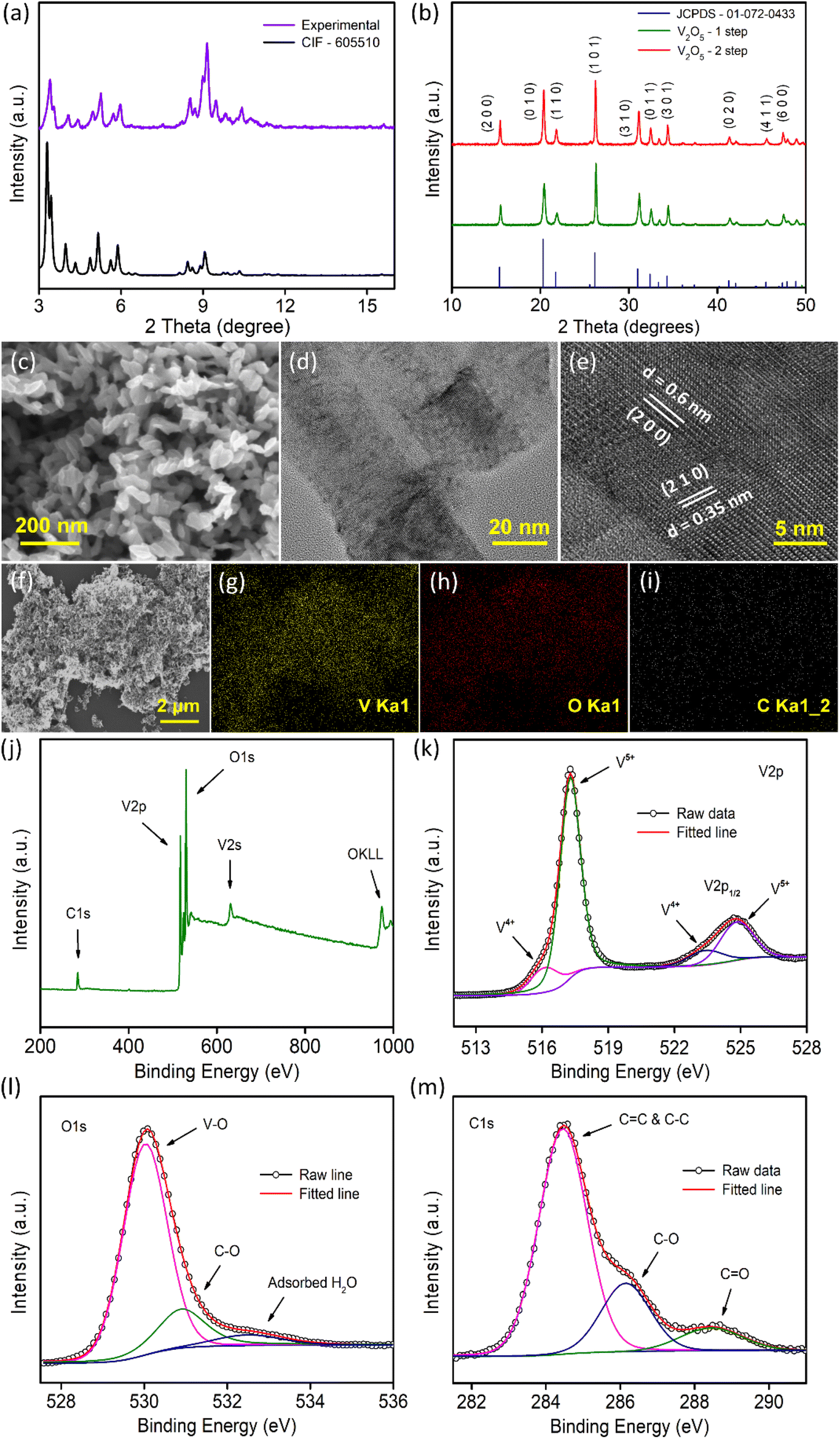 | ||
| Fig. 1 (a) XRD pattern of the activated V-MOF (purple) and the reported data CIF – 605510; (b) XRD data of V2O5 samples along with JCPDS card (01-072-0433) data; (c) FESEM image, (d) TEM image, (e) HRTEM image of the V2O5-1 sample and (f–i) EDX data for its elemental mapping, (j) XPS survey spectrum of the V2O5-1 sample and deconvoluted XPS spectra of (k) V 2p, (l) O 1s and (m) C 1s levels. | ||
Morphological characterization of the samples was conducted by FESEM and TEM measurements. Fig. 1c illustrates the morphology of the V2O5-1 sample and the sample mainly consists of irregularly shaped V2O5 nanoplates of dimensions ranging between 30 and 90 nm. A lower magnification TEM image is presented in Fig. 1d, which is concurrent with the FESEM images, exhibiting the presence of very thin nanoplates in the sample. The high-resolution TEM (HR-TEM) data (Fig. 1e) of the sample depicts the presence of lattice fringes with spacings of 0.35 and 0.6 nm which correspond to the (210) and (200) crystal planes of orthorhombic V2O5, respectively. A similar sort of morphology was also observed for the V2O5-2 sample, as illustrated in Fig. S2a–2c.† Furthermore, EDX mapping measurements were performed on both samples to check the presence of different elements e.g., elemental carbon along with vanadium and oxygen as shown in Fig. 1f–i (and in Fig. S2d–2g†). Carbon mapping images (Fig. 1i and Fig. S2g†) of both samples look almost similar and a very small amount of carbon was observed. The amount of carbon in both samples was quantified using XPS measurements as discussed later.
Raman spectroscopy measurements were carried out on both samples. Raman spectra (Fig. S3†) highlight several well-resolved peaks at ∼145, 199, 286, 305, 405, 482, 527, 703 and 995 cm−1 which are the characteristic peaks of crystalline V2O5. The vibrational Raman active modes are associated with vanadium–oxygen–vanadium bending vibrations, translational modes and vanadium–oxygen stretching modes. The highest intensity peak centered at 145 cm−1 corresponds to the bond deformation between different molecular units in the plane of layers, also termed the skeleton bending vibration. The peak at 995 cm−1 is attributed to the stretching mode vibration related to the V![[double bond, length as m-dash]](https://www.rsc.org/images/entities/char_e001.gif) O bond.45
O bond.45
The surface chemical states of the V2O5 samples were analyzed through XPS measurements as presented in Fig. 1j–m and Fig. S4.†Fig. 1j and Fig. S4a† present the survey spectra of the samples which show the peaks corresponding to the vanadium, oxygen and carbon in the sample in accordance with the EDX mapping data (Fig. 1f–i). From XPS measurement, the carbon content in V2O5-1 and V2O5-2 samples were quantified and found to be almost in the similar range of 12.43% and 12.47%, respectively. The core level spectra of V 2p show two major peaks at 517.2 eV and 524.8 eV, which correspond to V 2p1/2 and V 2p3/2 (Fig. 1k and Fig. S4b†). On deconvolution, the weaker and broader peaks at 516.3 eV and 523.6 eV are related to the presence of V4+ oxidation states and the relatively stronger peaks (at 517.3 and 524.9 eV) are assigned to the V5+ states of V2O5.35,36,46 The O 1s spectra provided in Fig. 1l and Fig. S4c† can be deconvoluted into three peaks. The most intense peak at 530 eV corresponds to the existence of the V–O bond in V2O5. The peak that appeared at 531 eV is due to the C–O bond and the peak that emerged at 532.6 eV is related to either OC–O or the adsorbed H2O molecules.35,47–49Fig. 1m and Fig. S4d† present asymmetric C 1s peaks, which were resolved into three peaks. The dominant peak at 284.5 eV arises due to the presence of graphitized carbon (C–C and CC) in the sample generated due to the denaturation of the carbon skeleton during the annealing of the sample. The peak located at 286.1 eV is associated with the C–O bonds and the smallest peak at 288.5 eV is related to the CO groups.48,50 Therefore, XPS data conclude the presence of graphitized carbon in both samples in similar quantities.
Furthermore, N2 gas adsorption measurement (Fig. S5†) at 77 K was carried out to check the surface areas and pore size distributions of the V2O5 samples. The adsorption isotherms exhibit the typical mesoporous nature of the samples. The surface areas of the samples were calculated using the Brunauer–Emmett–Teller (BET) fitting (Fig. S5b and S5e†) and the specific surface area was found to be higher (178 m2 g−1) for the V2O5-1 sample than for the V2O5-2 sample (112 m2 g−1). The non-local pore size distribution (NLDFT) method was used to calculate the pore-size distribution of the samples as shown in Fig. S5c and S5f.† A longer annealing time of V2O5-2 (because of the 2-step annealing process) reduces the pore volume in comparison to the only air annealed V2O5-1 sample. Overall, the mesoporous structures of the samples are expected to ensure facile ion exchange with the electrolyte towards better electrochemical performance.
| V2O5 + xLi+ + xe− ↔ LixV2O5 (0 ≤ x ≤ 1) | (1) |
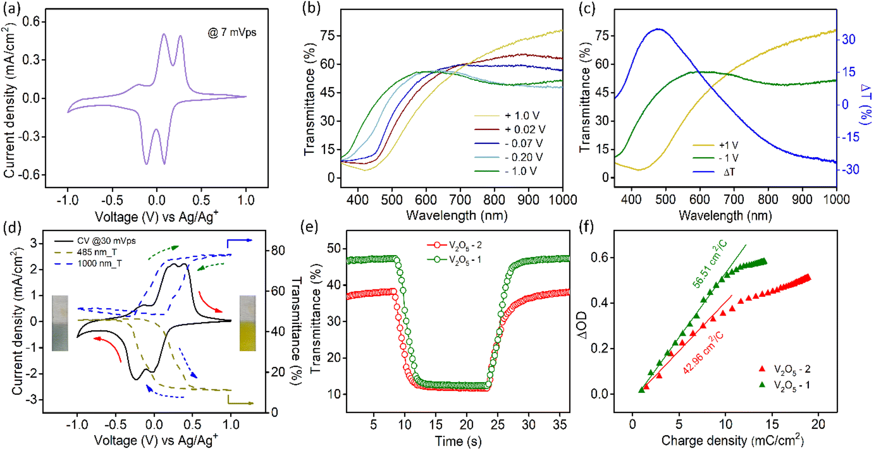 | ||
| Fig. 2 (a) Cyclic voltammogram (CV) of the V2O5-1 electrode in a three-electrode setup at a scan rate of 7 mV s−1 in a 1 M LiClO4/PC electrolyte, (b) transmission spectra of V2O5-1 films under different biases, (c) transmission of V2O5-1 films at two extreme potentials along with the transmission modulation spectrum (ΔT) (blue line), (d) CV data (solid line) of the V2O5-1 film with in situ transmittance data (dashed lines) at 485 nm (dark yellow) and at 1000 nm (blue), (e) switching times of V2O5-1 and V2O5-2 at 485 nm under an alternating potential with 15 s interval, and (f) coloration efficiency plot of both the samples. | ||
The transmission spectra of V2O5 samples were collected at different voltages during the cathodic scan (+1 V to −1 V vs. Ag/Ag+ electrode). Fig. 2b illustrates the transmission spectra of V2O5-1 electrodes. The corresponding photographs of the films at different voltages are shown in Fig. S6a.† The film reversibly switches its color from yellow (+1 V) to bluish gray (−1 V). Fig. 2c shows the transmission spectra at those two extreme potentials along with the optical modulation data (blue curve), which is defined as the difference between the transmittance at the colored and bleached states of an electrochromic material at a particular wavelength λ (i.e., ΔT = Tb(λ) − Tc(λ)). The analogous data for V2O5-2 electrodes are given in Fig. S6b.† Interestingly, it was observed for both the materials that the transmittance in the visible and near infrared regions changes reversibly upon applying voltages. Higher ΔT values of about 35% at 485 nm and 26.5% at 1000 nm were obtained for V2O5-1 electrodes. In the in situ spectroelectrochemistry measurement, the transmission modulation of the V2O5-1 film was closely monitored at 485 nm and 1000 nm, as illustrated in Fig. 2d (dotted lines). The dynamical changes of transmittances (indicated by arrows) are commensurate with the modulation of the current density.
Switching time for the electrochromic materials is described as the time required for attaining 90% of the total optical modulation under the application of an alternating potential. Switching times were measured at 485 nm (Fig. 2e) and 1000 nm (Fig. S7a†) wavelengths separately by applying +1 V and −1 V bias. The data for both samples are presented in Table 1. Although each sample contains graphitized carbon almost in close quantity; because of the higher surface area of the V2O5-1 sample, it manifests faster switching times compared to the V2O5-2 electrodes. The coloration efficiency (CE) of an electrochromic material is an important parameter in terms of estimating the power requirement for electrochromic switching. This is defined as the ratio of the change in the optical density (ΔOD) to the intercalated or deintercalated charge density (mC cm−2).54 CE can be calculated from the following formula stated as:
| CE = log (Tb/Tc)/(Q/A) | (2) |
| Sample | ΔT (%) | Coloring time (s) | Bleaching time (s) | Coloration eff. (cm2 C−1) | ||||
|---|---|---|---|---|---|---|---|---|
| 485 nm | 1000 nm | 485 nm | 1000 nm | 485 nm | 1000 nm | 485 nm | 1000 nm | |
| V2O5-2 | 28.5 | 20.4 | 3 | 2.4 | 5.3 | 3.2 | 42.96 | 13.1 |
| V2O5-1 | 35 | 26.5 | 2.9 | 2.1 | 3.4 | 2.6 | 56.51 | 24.5 |
CE values were calculated at 485 nm and 1000 nm from the slope of the ΔOD vs. charge density graphs, as shown in Fig. 2f and Fig. S7b.† The obtained CE values for both material electrodes are presented in Table 1. V2O5-1 electrodes excel over V2O5-2 electrodes, since their higher surface area provides a lot more active faradaic sites for facile electrochemical reactions.
| i = a1υ + a2υ1/2 | (3) |
 | ||
| Fig. 3 (a) Scan rate dependent CV data and in the inset log(i) vs. log(υ) plot, (b) GCD plots at different current densities, and (c) comparison of areal capacitances calculated from CV and GCD measurements, (d) in situ transmission data at 485 nm synchronized with the GCD data at different current densities. | ||
From the slope and intercept of the graph, i/υ1/2vs. υ1/2 (Fig. S10a†), a1 and a2 coefficients are determined and in the histogram plot of Fig. S10b,† deconvoluted current contributions are presented at different scan rates.33 With an increase in the scan rate, the contribution of diffusion towards the total current gradually decreases as Li+ ions do not get sufficient time to intercalate into the material.
Galvanostatic charge–discharge (GCD) data (Fig. 3b) for V2O5-1 electrodes were recorded over a potential window of +1 V to −1 V (vs. Ag/Ag+) at varying current densities from 0.02 mA cm−2 to 0.7 mA cm−2. The non-linear discharge curves consist of different segments – (a) an IR drop at the start of discharge can be seen due to the internal resistance of the system, (b) a steep linear section is due to the electrical double layer formation and (c) the plateau regions in each segment of the GCD profiles, which arise due to the faradaic reactions, confirming the pseudocapacitive nature of V2O5.59,60 The areal capacitances were calculated from the charge–discharge data according to the standard formula presented as follows:61
| Ca = (I × Δt)/(A × ΔV) | (4) |
 | (5) |
 is the area under the curve of a CV at a specific scan rate, υ is the scan rate of CV, A is the geometrical area of the electrode and Δv is the potential window in which CV is recorded. The areal capacitance values obtained from CV curves vary from 14.6 to 12.64 mF cm−2 with scan rates ranging from 2 to 70 mV s−1 and these values are presented in Fig. 3c to confirm the agreement of results derived from both CV and GCD techniques. In situ optical response at 485 nm synchronized with the GCD curves at two different current densities are presented in Fig. 3d. During charging the color of the electrode turns yellow and the corresponding transmittance goes down, while the color gradually changes to bluish gray during discharging and the transmittance goes up. Overall, an optical contrast value of ∼34% at 485 nm is exhibited by the V2O5-1 electrode upon charging–discharging.
3.2. Positive electrode material (PANI)
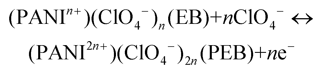
PANI consists of two main repeating units, namely reduced benzenoid and oxidized quinoid rings, the relative abundance of which decides the oxidation states and the electrical and optical properties of PANI.63 PANI exists in three discernible oxidation states. During electrochemical reactions it switches between these states and gives rise to different colors and properties. The three prominent states are as follows: (i) completely reduced leucoemeraldine base (LB) state containing only benzenoid units, which is nearly transparent or light yellow in color, (ii) fully oxidized pernigraniline base (PEB) state (blue in color) consisting of repeated units of benzenoid and quinoid rings and (iii) partially oxidized emeraldine base (EB) state (green in color) which is the most stable form of PANI in ambient atmosphere.63,64| PANI (LB) + nClO4− ↔ (PANIn+)(ClO4−)n (EB) + ne− |
 | (6) |
Two pairs of redox peaks arise in the CV profile of PANI due to the doping/dedoping of anions, as presented in Fig. S12.† The first redox couple at lower potentials is attributed to the transition between the LB and EB states and the second pair of peaks is due to the switch between the EB and PEB states as described in the above reactions.
The transmission spectra of PANI electrodes at different potentials (during anodic scan from −1 V to +1 V vs. Ag/Ag+ electrode) are shown in Fig. S13a.† The corresponding film photographs are displayed in Fig. S13b.† The transmission data at two terminal potentials (+1 V and −1 V vs. Ag/Ag+) and the corresponding optical modulation spectra are plotted in Fig. S13c.† The highest change in transmittance in PANI films was found to be nearly 75% at 650 nm. Supporting this, in situ optical modulation of the film at 650 nm was measured by CV at a scan rate of 30 mV s−1, as shown in Fig. S13d.†
Scan rate dependent CV data for the PANI electrode are shown in Fig. S14a.† Fig. S14b† presents the log(i) vs. log(υ) plot and b value comes out to be nearly 0.9. Furthermore, it can be concluded from the plots shown in Fig. S14d† that although the current density of PANI films mostly emerges due to the capacitive process, the contribution also comes from the intercalation of ions into the material. Fig. S15a† presents the GCD data of the PANI film at varying current densities. The areal capacitance value ranges from 13.69 mF cm−2 to 11.1 mF cm−2 as the current density switches from 0.02 mA cm−2 to 0.7 mA cm−2. Similar to the V2O5 electrodes, the charge–discharge profiles in this case are also non-linear, which points towards the presence of surface-controlled faradaic processes. The areal capacitance values for PANI films were also extracted from CV curves according to eqn (5). The highest value obtained was 12.3 mF cm−2 at a scan rate of 10 mV s−1. The obtained values are compared in Fig. S15b.† With the increase in the scan rate of CV or the current density in charge–discharge, the areal capacitance value decreases due to the inaccessibility of reaction sites of the active material.67 The in situ change in transmittance at 650 nm during charging–discharging of PANI electrodes at different current densities is presented in Fig. S15c.† During charging, the structural units of PANI get oxidized, which demands doping of ClO4− ions into the film to maintain the charge balance and this process is accompanied by a transmission drop in PANI films. Removal of electrons along with the movement of charge balancing counter anions causes structural changes in the polymeric chains, leading to the evolution of positively charged polaronic and bipolaronic states. Oxidation of conducting polymers leads to the generation of mid bandgap states and successively creates new lower energy electronic transitions lying in the near-infrared wavelength range.68,69 During discharging, the reduction of PANI takes place with the simultaneous return of ClO4− ions to the solution and the film gains its transparency again.
3.3. Multi-colored electrochromic asymmetric supercapacitor (MECASC)
CV curves collected for both V2O5 and PANI electrodes in a 1 M LiClO4/PC electrolyte in a three-electrode setup are presented in Fig. 4a, which sustains our choice of using V2O5 as a negative electrode and PANI as a positive electrode in assembling a MECASC for a voltage window up to 2 V. To obtain better performance from an ASC, the charge balance between its two electrodes should be maintained; i.e., q+ = q−, where q+ and q− correspond to the charges of positive and negative electrodes, respectively, and q = I × Δt, where I and Δt are as defined earlier. To do that, the first step was to take the charge–discharge profile of the V2O5 electrode at a fixed current density, and then accordingly the electrodeposition time (150 s) of the PANI film was adjusted such that the capacity of the PANI film matches the capacity of V2O5.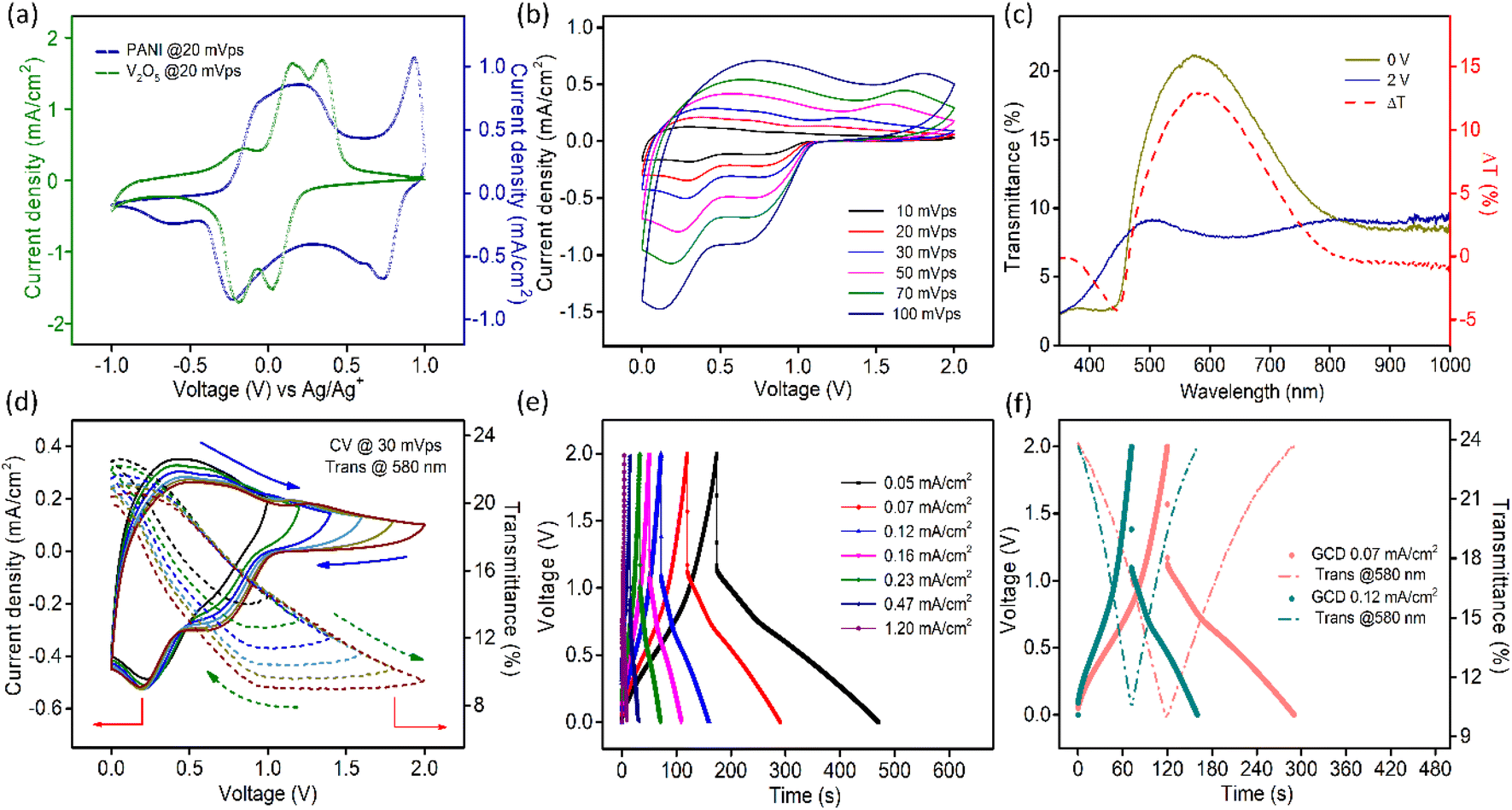 | ||
| Fig. 4 (a) CV of PANI and V2O5 electrodes separately measured in a three-electrode setup in the identical voltage window (±1 V vs. Ag/Ag+) with a 1 M LiClO4/PC electrolyte at a scan rate of 20 mV s−1; (b) CV of the MECASC measured in a two-electrode setup at varying scan rates; (c) transmission spectra of the device at two terminal voltages and the optical modulation spectra (dotted line); and (d) CV at varying potential windows with simultaneous in situ transmission changes at 580 nm; (e) GCD profiles at different current densities, and (f) in situ transmission changes at 580 nm in harmony with GCD profiles at two different current densities. | ||
| Positive electrode – (PANI2nx+)(ClO4−)2nx + 2ne− ↔ PANI + 2nClO4− | (7) |
| Negative electrode – LixV2O5 ↔ V2O5 + xLi+ + nxe− | (8) |
 | (9) |
The contribution of faradaic and surface controlled processes of current was investigated, as shown in Fig. S16a–c.† The plots of log(i) vs. log(υ) at different voltages are given in Fig. S16a† and the extracted b values signify that the overall reaction is dominated by a surface-controlled capacitive process. The separation of capacitive and diffusive contributions of current at different scan rates is presented in Fig. S16c.†
The transmission spectra of the MECASC were recorded at different voltages during anodic and cathodic scans within the voltage window of 0–2 V, Fig. S17a and b.† Transmission spectra at the end voltages and the optical modulation spectra of the system are shown in Fig. 4c. Transmission modulation reaches a highest value of ∼13.5% at 580 nm. At 0 V, the whole system looks yellowish green in color (individually, V2O5 and PANI film colors are yellow and yellowish green, respectively) and with the increase in applied bias, PANI and V2O5 gradually become oxidized and reduced, respectively. As a consequence, the color of the device changes to dark blue (where V2O5 and PANI films change to bluish gray and dark blue color, respectively).
CV profiles (at 30 mV s−1 sweep rate) at different working voltage windows are presented in Fig. 4d along with the dynamic changes in transmissions at 580 nm, which are well consistent with the change in current density. As the voltage window increases beyond 1 V, surface-redox reactions start to appear prominently, accompanied by an increase in optical modulation value up to 40% of its initial value as depicted in Fig. 4d. When operational voltage gradually increases from 1 to 2 V, the energy density calculated according to the equation, E = 1/2 × CV2, elevates from 1.17 × 10⁻³ to 2.93 × 10⁻³ mW h cm−2.
GCD measurements (Fig. 4e) of the MECASC module were performed at different current densities ranging from 0.05 to 1.2 mA cm−2 within the operational voltage window of 2 V. The presence of nonlinearity in GCD profiles indicates the existence of faradaic reactions in PANI and V2O5. The areal capacitance touches a maximum value of 12.27 mF cm−2 at a current density of 0.05 mA cm−2 with an energy density of 2.21 × 10⁻³ mW h cm−2. At a 24 times higher current density of 1.2 mA cm−2, 58.2% areal capacitance value i.e., 7.14 mF cm−2 can be retained compared to that at 0.05 mA cm−2 and the energy density decreases to 5.7 × 10⁻⁴ mW h cm−2. Fig. 4f presents the optical modulation synced with GCD profiles at two different current densities. Optical modulation at 580 nm reduces from 13.7% to 12.9% with an increase in the current density from 0.07 to 0.12 mA cm−2 with a simultaneous decrement in areal capacitance from 10.63 to 9.52 mF cm−2. The probable reason behind this is the inaccessibility of active electrode materials for charge storage as there is a limitation in the migration of ionic species with the increase in the current density.71
Fig. 5a shows the GCD profile of the MECASC at a current density of 0.12 mA cm−2. The photographs of the module are presented in Fig. 5b at different instants of charging and discharging as shown by the red circles in the GCD curve in Fig. 5a. This well coordinated behavior of color changes (yellowish green, dark green, greenish blue, blue and dark blue) during charging–discharging of the electrode helps to uniquely identify the state of charge of the system. To further understand the performance of the MECASC system, the switching times and the coloration efficiency were calculated. Switching times were determined according to the description previously given in section 3.1.2, by applying potentials alternating between 0 V and 2 V. Calculated coloration and bleaching times of the system were 16.4 s and 12.9 s, respectively. Furthermore, the coloration efficiency (CE) was calculated at 580 nm wavelength according to eqn (2) and a high CE value of 137.2 cm2 C−1 was obtained for the module.
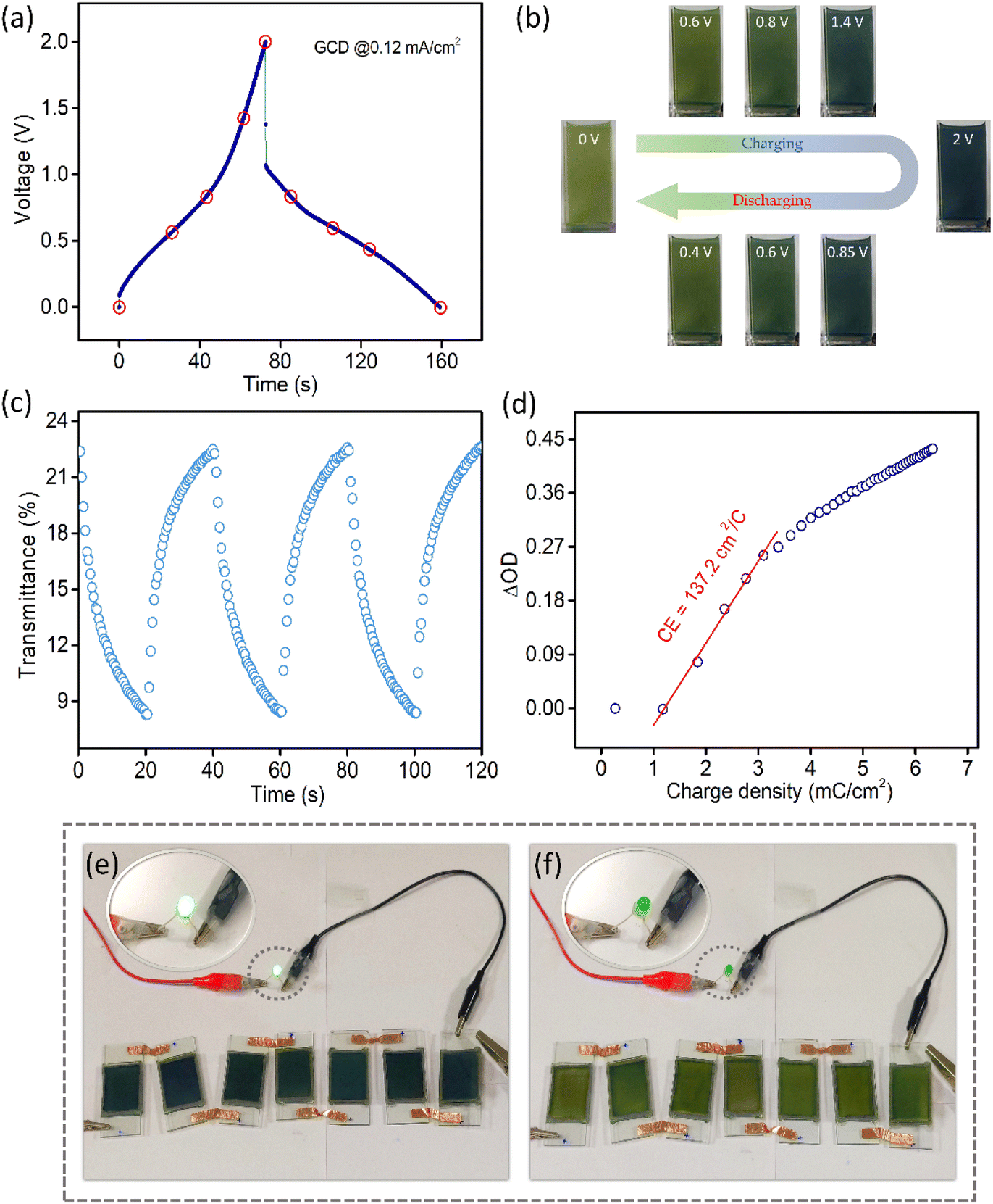 | ||
| Fig. 5 (a) GCD profile of the MECASC at a current density of 0.12 mA cm−2, (b) photographs of the system at different voltages during charging and discharging as assigned by the red circles in (a); (c) switching times of the module at 580 nm by applying 0 V and 2 V potential alternatively with 20 s interval; (d) coloration efficiency of the system at 580 nm; and photographs demonstrate (e) charged and (f) discharged states of the devices, connected in series; insets show the state of the LED in both cases. | ||
Cycling performance is a measure of the life span of a device for practical applications. By conducting the cycling stability measurement at a high current density of 1 mA cm−2, it is observed that the supercapacitor can sustain nearly 50% of its initial capacitance value after 7000 cycles (Fig. S18a†). This kind of capacity decay is quite common among V2O5 electrodes.50,53,72,73 The galvanostatic charge–discharge (GCD) curves of the module at a current density of 0.12 mA cm−2 along with the dynamic change of its transmission at 580 nm wavelength before and after cycling are presented in Fig. S18b.† After cycling, the transmission modulation value at 580 nm reduces by ∼18.47% of its initial value. There is a lowering in transmittance of the bleached state, which may be caused due to the trapped charge inside the electrodes because of repeated cycling.74,75 The morphologies of both V2O5 and PANI films were examined by the FESEM technique. Fig. S19 and S20† present the FESEM images of V2O5 and PANI electrodes, respectively, at different magnifications (10 μm and 1 μm) before and after cycling. For the V2O5 electrode, dark patches were noticed on the films after cycling as presented in Fig. S19c and S19d,† which are absent in the image, illustrated in Fig. S19a and S19b† before cycling. The patches could be the portions of the electrode from where chunks of electrode materials were peeled off during cycling. Fig. S19b and S19d† illustrate these aspects with better clarity. This occurs due to the mechanical stress generated during ion intercalation–deintercalation,76 causing capacity fading for V2O5-based materials as mentioned in previous reports.30,77,78 Additionally, no visible color change of the electrolyte was noted after the cycling test. According to other literature reports, V2O5 tends to dissolve in an aqueous electrolyte during cycling;47,51 in contrast, organic electrolytes effectively decrease the dissolution of V2O5 and increase the stability of the electrodes.51 From Fig. S20a and S20c,† not much change in the PANI electrode is observed before and after cycling. A closer inspection reveals that the diameters of the pores in the PANI film increased after cycling as presented in Fig. S20b and S20d.†
Prototypes of the MECASC (2.5 cm × 4 cm) were assembled to demonstrate the practical applicability. The devices were connected in series, which lit up the green LED for almost 7 min (video provided in the ESI†). The photograph of the devices is presented in Fig. 5e in their charged states with a glowing green LED. Fig. 5f shows the discharged state of the devices with a yellowish green color and an LED in the off state.
4. Conclusion
MOF-derived V2O5 has been successfully synthesized and employed as an electrochromic electrode, which shows large optical modulations with very fast switching times and decent coloration efficiencies. Later, the V2O5 film was used as the negative electrode for the fabrication of a multicolored electrochromic asymmetric supercapacitor alongside an electrodeposited PANI film, which was deployed as the positive electrode. Owing to its multiple-colored states at different stages of charging and discharging, it enables the direct determination of its energy storage level with the naked eye. As an electrochromic energy storage device, it demonstrates a high coloration efficiency of 137.2 cm2 C−1 and an areal capacitance of 12.27 mF cm−2 with an energy density of 2.21 × 10⁻³ mW h cm−2 at a current density of 0.05 mA cm−2. Moreover, this operates as an energy-efficient EC device by eliminating the requirement of energy during bleaching as it recycles the energy stored during charging. In a nutshell, this work is a new stride towards the intelligent automation of energy storage devices.Conflicts of interest
The authors declare no financial interest.Acknowledgements
We want to thank Mr Shriniwas Deo from the CSIR-National Chemical Laboratory (CSIR-NCL, Pune) for his help with the XPS measurement. We sincerely thank Prof. Sujit K. Ghosh and his student Dr Subhajit Dutta from the Department of Chemistry, IISER Pune, for helping us with the gas adsorption measurements of the samples. A. D. thanks Dr Sattwick Haldar for helping with the fitting of adsorption data. A. D. acknowledges Dr Atikur Rahman and his students Mr Gokul M. A. and Mr Tamaghna Chowdhury from the Department of Physics, IISER Pune, for helping with the tube furnace setup in their lab. A. D. thanks Mr Soumodip Sur for his cooperation during the work. A. D. acknowledges the INSPIRE fellowship from the DST, India. R. N. acknowledges funding from the Department of Science Technology, India, through the INSPIRE faculty scheme (DST/INSPIRE/04/2017/002761). M. O. T. is indebted to the DST-SERB (CRG/2020/002549), the DST-WTI (DST/TMD-EWO/WTI/2K19/EWFH/2019/272) and the DST-HFC (DST/TMD/HFC/2K18/58) for financial support.References
- A. Eftekhari, ACS Sustainable Chem. Eng., 2019, 7, 5602–5613 CrossRef CAS.
- Q. Zhang, B. He, L. Tang, Z. Zhou, L. Kang, J. Sun, T. Zhang, Q. Li, C. Li, J. Zhao, Z. Zhang, L. Wei and Y. Yao, Adv. Funct. Mater., 2019, 29, 1808889 CrossRef.
- A. Fakharuddin, R. Jose, T. M. Brown, F. Fabregat-Santiago and J. Bisquert, Energy Environ. Sci., 2014, 7, 3952–3981 RSC.
- S. Cavaliere, S. Subianto, I. Savych, D. J. Jones and J. Rozière, Energy Environ. Sci., 2011, 4, 4761–4785 RSC.
- J. Yuan, M. Qiu, X. Hu, Y. Liu, G. Zhong, H. Zhan and Z. Wen, ACS Nano, 2022, 16, 14807–14818 CrossRef CAS PubMed.
- Y. Liu, X. Hu, J. Li, G. Zhong, J. Yuan, H. Zhan, Y. Tang and Z. Wen, Nat. Commun., 2022, 13, 663 CrossRef CAS PubMed.
- L. J. Wang, M. F. El-Kady, S. Dubin, J. Y. Hwang, Y. Shao, K. Marsh, B. McVerry, M. D. Kowal, M. F. Mousavi and R. B. Kaner, Adv. Energy Mater., 2015, 5, 1500786 CrossRef.
- P. Simon and Y. Gogotsi, Nat. Mater., 2008, 7, 845–854 CrossRef CAS PubMed.
- T. Zhu, Y. Yang, Y. Liu, R. Lopez-Hallman, Z. Ma, L. Liu and X. Gong, Nano Energy, 2020, 78, 105397 CrossRef CAS.
- P. Xie, W. Yuan, X. Liu, Y. Peng, Y. Yin, Y. Li and Z. Wu, Energy Storage Mater., 2021, 36, 56–76 CrossRef.
- Y. Huang, M. Zhu, Z. Pei, Q. Xue, Y. Huang and C. Zhi, J. Mater. Chem. A, 2016, 4, 1290–1297 RSC.
- Y. Jiang, M. Cheng, R. Shahbazian-Yassar and Y. Pan, Adv. Mater. Technol., 2019, 4, 1900691 CrossRef CAS.
- X. Liang, L. Zhao, Q. Wang, Y. Ma and D. Zhang, Nanoscale, 2018, 10, 22329–22334 RSC.
- Q. Guo, X. Zhao, Z. Li, D. Wang and G. Nie, Chem. Eng. J., 2020, 384, 123370 CrossRef CAS.
- J. Chen, Z. Wang, Z. Chen, S. Cong and Z. Zhao, Nano Lett., 2020, 20, 1915–1922 CrossRef CAS PubMed.
- Z. Lu, X. Zhong, X. Liu, J. Wang and X. Diao, Phys. Chem. Chem. Phys., 2021, 23, 14126–14145 RSC.
- H. Wang, C.-J. Yao, H.-J. Nie, L. Yang, S. Mei and Q. Zhang, J. Mater. Chem. C, 2020, 8, 15507–15525 RSC.
- Y. Zhong, Z. Chai, Z. Liang, P. Sun, W. Xie, C. Zhao and W. Mai, ACS Appl. Mater. Interfaces, 2017, 9, 34085–34092 CrossRef CAS PubMed.
- Q. Guo, J. Li, B. Zhang, G. Nie and D. Wang, ACS Appl. Mater. Interfaces, 2019, 11, 6491–6501 CrossRef CAS PubMed.
- Q. Guo, X. Zhao, Z. Li, B. Wang, D. Wang and G. Nie, ACS Appl. Energy Mater., 2020, 3, 2727–2736 CrossRef CAS.
- N. Kobayashi, S. Miura, M. Nishimura and H. Urano, Sol. Energy Mater. Sol. Cells, 2008, 92, 136–139 CrossRef CAS.
- J. Padilla, V. Seshadri, T. F. Otero and G. A. Sotzing, J. Electroanal. Chem., 2007, 609, 75–84 CrossRef CAS.
- J. Wang, L. Zhang, L. Yu, Z. Jiao, H. Xie, X. W. Lou and X. W. Sun, Nat. Commun., 2014, 5, 4921 CrossRef CAS PubMed.
- S. Mishra, P. Yogi, P. R. Sagdeo and R. Kumar, ACS Appl. Energy Mater., 2018, 1, 790–798 CrossRef CAS.
- G. Cai, P. Darmawan, X. Cheng and P. S. Lee, Adv. Energy Mater., 2017, 7, 1602598 CrossRef.
- W. Zhang, H. Li, W. W. Yu and A. Y. Elezzabi, Small Sci., 2021, 1, 2100040 CrossRef CAS.
- S. B. Singh, D. T. Tran, K.-U. Jeong, N. H. Kim and J. H. Lee, Small, 2022, 18, 2104462 CrossRef CAS PubMed.
- H. Liang, R. Li, C. Li, C. Hou, Y. Li, Q. Zhang and H. Wang, Mater. Horiz., 2019, 6, 571–579 RSC.
- L. Zhao, J. Kuang, W. Zhuang, J. Chao, W. Liao, X. Fu, C. Li, L. Ye and H. Liu, Nanotechnology, 2021, 33, 054001 CrossRef PubMed.
- S. Zhang, S. Chen, Y. Luo, B. Yan, Y. Gu, F. Yang and Y. Cao, J. Alloys Compd., 2020, 842, 155882 CrossRef CAS.
- D. Majumdar, M. Mandal and S. K. Bhattacharya, ChemElectroChem, 2019, 6, 1623–1648 CrossRef CAS.
- M. M. Margoni, S. Mathuri, K. Ramamurthi, R. R. Babu, V. Ganesh and K. Sethuraman, Appl. Surf. Sci., 2018, 449, 193–202 CrossRef CAS.
- A. Dewan, S. Sur, R. Narayanan and M. O. Thotiyl, ChemElectroChem, 2022, 9, e202200001 CrossRef CAS.
- R. R. Salunkhe, Y. V. Kaneti and Y. Yamauchi, ACS Nano, 2017, 11, 5293–5308 CrossRef CAS PubMed.
- Y.-S. Hsiao, C.-W. Chang-Jian, W.-L. Syu, S.-C. Yen, J.-H. Huang, H.-C. Weng, C.-Z. Lu and S.-C. Hsu, Appl. Surf. Sci., 2021, 542, 148498 CrossRef CAS.
- T. Q. He, J. H. Li, Z. Z. Luo, Y. Q. Zhang, Y. Y. Zhao, X. T. Zhang and Y. J. Chen, ChemElectroChem, 2022, 9, e202200178 CAS.
- Y. Ding, Y. Peng, W. Chen, Y. Niu, S. Wu, X. Zhang and L. Hu, Appl. Surf. Sci., 2019, 493, 368–374 CrossRef CAS.
- T. Kim, H. Kim, T.-S. You and J. Kim, J. Alloys Compd., 2017, 727, 522–530 CrossRef CAS.
- W. Li, J. Wang, J. Chen, K. Chen, Z. Wen and A. Huang, Small, 2022, 18, 2202018 CrossRef CAS PubMed.
- F. Carson, J. Su, A. E. Platero-Prats, W. Wan, Y. Yun, L. Samain and X. Zou, Cryst. Growth Des., 2013, 13, 5036–5044 CrossRef CAS.
- Y. Mohd, R. Ibrahim and M. F. Zainal, Presented in part at the 2012 IEEE Symposium on Humanities, Science and Engineering Research, Kuala Lumpur, 24–27 June 2012, 2012.
- P. Yilmaz, M. Magni, S. Martinez, R. M. Gonzalez Gil, M. Della Pirriera and M. Manca, ACS Appl. Energy Mater., 2020, 3, 3779–3788 CrossRef CAS.
- G. Férey, C. Mellot-Draznieks, C. Serre, F. Millange, J. Dutour, S. Surblé and I. Margiolaki, Science, 2005, 309, 2040–2042 CrossRef PubMed.
- S. Biswas, S. Couck, M. Grzywa, J. F. M. Denayer, D. Volkmer and P. Van Der Voort, Eur. J. Inorg. Chem., 2012, 2012, 2481–2486 CrossRef CAS.
- W.-C. Fang, J. Phys. Chem. C, 2008, 112, 11552–11555 CrossRef CAS.
- Y. Chen, K. Muthukumar, L. Leban and J. Li, Electrochim. Acta, 2020, 330, 135200 CrossRef CAS.
- H. Liu, W. Zhu, D. Long, J. Zhu and G. Pezzotti, Appl. Surf. Sci., 2019, 478, 383–392 CrossRef CAS.
- M. Sathiya, A. S. Prakash, K. Ramesha, J. M. Tarascon and A. K. Shukla, J. Am. Chem. Soc., 2011, 133, 16291–16299 CrossRef CAS PubMed.
- C. Y. Foo, A. Sumboja, D. J. H. Tan, J. Wang and P. S. Lee, Adv. Energy Mater., 2014, 4, 1400236 CrossRef.
- M. Li, G. Sun, P. Yin, C. Ruan and K. Ai, ACS Appl. Mater. Interfaces, 2013, 5, 11462–11470 CrossRef CAS PubMed.
- H. Zhang, X. Han, R. Gan, Z. Guo, Y. Ni and L. Zhang, Appl. Surf. Sci., 2020, 511, 145527 CrossRef CAS.
- B. D. Boruah, B. Wen and M. De Volder, Nano Lett., 2021, 21, 3527–3532 CrossRef CAS PubMed.
- J. Yang, T. Lan, J. Liu, Y. Song and M. Wei, Electrochim. Acta, 2013, 105, 489–495 CrossRef CAS.
- A. Dewan, S. Haldar and R. Narayanan, J. Solid State Electrochem., 2021, 25, 821–830 CrossRef CAS.
- M. Holzapfel, A. Martinent, F. Alloin, B. Le Gorrec, R. Yazami and C. Montella, J. Electroanal. Chem., 2003, 546, 41–50 CrossRef CAS.
- S. K. Meher, P. Justin and G. Ranga Rao, Nanoscale, 2011, 3, 683–692 RSC.
- V. Lvovich, in Impedance Spectroscopy: Applications to Electrochemical and Dielectric Phenomena, John Wiley & Sons, 2012, pp. 281–318, DOI:10.1002/9781118164075.ch12.
- H. Lee, V. S. Kumbhar, J. Lee, Y. Choi and K. Lee, Electrochim. Acta, 2020, 334, 135618 CrossRef CAS.
- Y. Zhang, J. Zheng, Y. Zhao, T. Hu, Z. Gao and C. Meng, Appl. Surf. Sci., 2016, 377, 385–393 CrossRef CAS.
- B. Pandit, D. P. Dubal, P. Gómez-Romero, B. B. Kale and B. R. Sankapal, Sci. Rep., 2017, 7, 43430 CrossRef PubMed.
- J. Pan, R. Zheng, Y. Wang, X. Ye, Z. Wan, C. Jia, X. Weng, J. Xie and L. Deng, Sol. Energy Mater. Sol. Cells, 2020, 207, 110337 CrossRef CAS.
- M. Qiu, P. Sun, L. Shen, K. Wang, S. Song, X. Yu, S. Tan, C. Zhao and W. Mai, J. Mater. Chem. A, 2016, 4, 7266–7273 RSC.
- M. Beygisangchin, S. Abdul Rashid, S. Shafie, A. R. Sadrolhosseini and H. N. Lim, Polymers, 2021, 13, 2003 CrossRef CAS PubMed.
- S. F. Kuchena and Y. Wang, ACS Appl. Energy Mater., 2020, 3, 11690–11698 CrossRef CAS.
- X. Wu, Q. Wang, W. Zhang, Y. Wang and W. Chen, Synth. Met., 2016, 220, 494–501 CrossRef CAS.
- K. Xu, Q. Zhang, Z. Hao, Y. Tang, H. Wang, J. Liu and H. Yan, Sol. Energy Mater. Sol. Cells, 2020, 206, 110330 CrossRef CAS.
- K. Zhou, H. Wang, J. Jiu, J. Liu, H. Yan and K. Suganuma, Chem. Eng. J., 2018, 345, 290–299 CrossRef CAS.
- A. L. Dyer, A. M. Österholm, D. E. Shen, K. E. Johnson and J. R. Reynolds, in Electrochromic Materials and Devices, ed. R. J. Mortimer, D. R. Rosseinsky and P. M. S. Monk, Wiley-VCH Verlag GmbH & Co. KGaA, 2015, pp. 113–184 Search PubMed.
- W. T. Neo, M. H. Chua and J. W. Xu, in Electrochromic Smart Materials: Fabrication and Applications; Smart Materials Series, ed. J. W. Xu, M. H. Chua and K. W. Shah, The Royal Society of Chemistry, 2019, pp. 22–50 Search PubMed.
- K. Subramani, N. Sudhan, R. Divya and M. Sathish, RSC Adv., 2017, 7, 6648–6659 RSC.
- G. Cai, P. Darmawan, M. Cui, J. Wang, J. Chen, S. Magdassi and P. S. Lee, Adv. Energy Mater., 2016, 6, 1501882 CrossRef.
- F. Azadian and A. C. Rastogi, Electrochim. Acta, 2020, 330, 135339 CrossRef CAS.
- B. Saravanakumar, K. K. Purushothaman and G. Muralidharan, ACS Appl. Mater. Interfaces, 2012, 4, 4484–4490 CrossRef CAS PubMed.
- J. Guo, M. Wang, X. Diao, Z. Zhang, G. Dong, H. Yu, F. Liu, H. Wang and J. Liu, J. Phys. Chem. C, 2018, 122, 19037–19043 CrossRef CAS.
- E. Hopmann, H. Li and A. Y. Elezzabi, RSC Adv., 2019, 9, 32047–32057 RSC.
- B. Saravanakumar, K. K. Purushothaman and G. Muralidharan, J. Electroanal. Chem., 2015, 758, 111–116 CrossRef CAS.
- W. Zhang, H. Li, M. Al-Hussein and A. Y. Elezzabi, Adv. Opt. Mater., 2020, 8, 1901224 CrossRef CAS.
- E. Umeshbabu and G. Ranga Rao, J. Colloid Interface Sci., 2016, 472, 210–219 CrossRef CAS PubMed.
Footnote |
| † Electronic supplementary information (ESI) available. See DOI: https://doi.org/10.1039/d2nr04841h |
| This journal is © The Royal Society of Chemistry 2022 |