
 Open Access Article
 This Open Access Article is licensed under a Creative Commons Attribution-Non Commercial 3.0 Unported Licence
Excitation and detection of acoustic phonons in nanoscale systems
Ryan C.
Ng
 *a,
Alexandros
El Sachat
*b,
Francisco
Cespedes
ac,
Martin
Poblet
a,
Guilhem
Madiot
a,
Juliana
Jaramillo-Fernandez
a,
Omar
Florez
ac,
Peng
Xiao
ac,
Marianna
Sledzinska
a,
Clivia M.
Sotomayor-Torres
ad and
Emigdio
Chavez-Angel
*a
*a,
Alexandros
El Sachat
*b,
Francisco
Cespedes
ac,
Martin
Poblet
a,
Guilhem
Madiot
a,
Juliana
Jaramillo-Fernandez
a,
Omar
Florez
ac,
Peng
Xiao
ac,
Marianna
Sledzinska
a,
Clivia M.
Sotomayor-Torres
ad and
Emigdio
Chavez-Angel
*a
aCatalan Institute of Nanoscience and Nanotechnology (ICN2), CSIC and BIST, Campus UAB, Bellaterra, 08193 Barcelona, Spain. E-mail: ryan.ng@icn2.cat; emigdio.chavez@icn2.cat
bNational Center for Scientific Research “Demokritos”, 15310 Athens, Greece. E-mail: alexandros.elsachat@icn2.cat
cDepartamento de Física, Universidad Autónoma de Barcelona, Bellaterra, 08193 Barcelona, Spain
dICREA, Passeig Lluis Companys 23, 08010 Barcelona, Spain
First published on 9th September 2022
Abstract
Phonons play a key role in the physical properties of materials, and have long been a topic of study in physics. While the effects of phonons had historically been considered to be a hindrance, modern research has shown that phonons can be exploited due to their ability to couple to other excitations and consequently affect the thermal, dielectric, and electronic properties of solid state systems, greatly motivating the engineering of phononic structures. Advances in nanofabrication have allowed for structuring and phonon confinement even down to the nanoscale, drastically changing material properties. Despite developments in fabricating such nanoscale devices, the proper manipulation and characterization of phonons continues to be challenging. However, a fundamental understanding of these processes could enable the realization of key applications in diverse fields such as topological phononics, information technologies, sensing, and quantum electrodynamics, especially when integrated with existing electronic and photonic devices. Here, we highlight seven of the available methods for the excitation and detection of acoustic phonons and vibrations in solid materials, as well as advantages, disadvantages, and additional considerations related to their application. We then provide perspectives towards open challenges in nanophononics and how the additional understanding granted by these techniques could serve to enable the next generation of phononic technological applications.
Introduction
Pioneering studies of confined acoustic waves were first performed by Lord Rayleigh1 in 1885. He demonstrated the existence of surface acoustic waves (SAWs) propagating along the surface of an isotropic solid half-space. These waves are non-dispersive and elliptically polarized in the sagittal plane, with velocities that are slightly smaller than that of bulk shear waves, and with amplitudes that decay exponentially, confining them to roughly within a wavelength of the surface. Following his results, other scientists further developed this topic, particularly: Stoneley,2 who described waves that propagate along the interface between two half-spaces, i.e., a generalization of Rayleigh modes; Love,3 who described horizontally polarized surface waves; and Sezawa,4 who demonstrated the existence of surface waves in layered structures. The propagation of SAW modes in these types of systems has been widely studied by the seismology community, who were the first to study the confinement of acoustic waves, although their relevance is pervasive and extends throughout modern devices.5 Years later, the acoustic properties of other finite systems and geometries were also studied. Pochhammer6 and Chree7 described the propagation of waves in infinite cylindrical rods. Lamb developed theoretical models to describe the natural vibration of spheres8 and suspended thin films.9 While all the aforementioned models were originally applied in “bulk-like” or macro-scale systems, the results are scale invariant and still hold down to the nano-10 and molecular11 scales.The quantization of the vibrational energy of an atom or a group of atoms in matter is a quasiparticle known as a phonon. As phonons are bosonic quasiparticles, they obey Bose–Einstein statistics and have an energy ħω and a pseudo-momentum p = ħq, where ω = 2πf, f is the phonon frequency, ħ is the reduced Planck constant (h/2π), and q is the wavevector.12 Similar to other quasiparticles, the wavelength dependence of the phonon energy can be represented by a dispersion relation, or a relationship between the phonon frequency and its wavevector. The phonon group velocity, vg = dω/dq, can be determined from the slope of a dispersion relation curve. For bulk material, the dispersion relation of acoustic phonons with short wavevector (i.e., near the Γ-point in the first Brillouin zone) is linear and the group velocity in the material is constant.13 Upon decreasing the characteristic dimensions of the material, this linear dependence no longer holds, and the phonon energy is quantized into many discrete modes. This spatial confinement resulting from the reduction of bulk material down to “finite” nanometer sizes affects a wide array of physical properties such as the phonon density of states, group velocity, specific heat capacity, and electron–phonon and phonon–phonon interactions, among others.14–19 Phonon statistics and the interaction of phonons with other particles sets a limit to properties such as the electrical and thermal conductivity, sound transmission, reflectivity of ionic crystals, the linewidth of semiconductor quantum dot emission, the maximum power that can be carried by optical fibers, and the inelastic scattering of light, X-rays, and neutrons.20,21 Thus, the engineering of new devices that are able to generate, control, and detect phonons becomes a key issue that is essential for the understanding and development of future technologies.
The elastic continuum model predicts that the acoustic/mechanical frequency scales inversely with the characteristic dimension of a structure. For example, the first natural mode of a solid sphere scales as 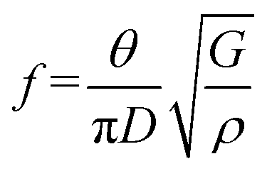 where θ is a root of a polynomial equation, D is the diameter, G is the shear modulus, and ρ is the density.8 As the size of the structure decreases, these modes increase in energy and can interact with particles or quasi-particles existing in the medium. Moreover, the decrease in size can also reduce the phonon mean free path due to diffusive scattering caused by the surface roughness of the boundaries. This has a direct impact on properties such as the thermal transport, where phonons are the main energy carriers in semiconductors and insulators. At the nanoscale, heat conduction is affected by: (i) the increase in boundary (interface) scattering and (ii) the effect of phonon confinement. At room temperature, the impact of phonon confinement on thermal transport is negligible. Rather, the modification of the thermal conductivity is mainly attributed to diffuse scattering of phonons at boundaries. Although this mechanism has been widely explored and exploited,22–24 recent works propose using phonon coherence to control heat flow.25–27 In this scenario, modification of the phonon dispersion relation by adding additional periodicity to the system by alternating thin layers of dissimilar materials (superlattices),28 patterning holes in a suspended system,29,30 or by self-assembling colloidal particles,31,32 offers a simple strategy to manipulate phonon waves. These kinds of systems are known as phononic crystals (PnCs) or acoustic metamaterials.
The generation, manipulation, and detection of phonons are three central concepts that are addressed by the phononic community, and their appropriate incorporation and consideration are essential towards realizing the aforementioned applications. Compared to its photonic and electronic counterparts, phononics has received less attention, in part due to the difficulty associated with the experimental excitation and detection of acoustic phonons. Beyond characterization of phonons, even the development and fabrication of platforms that operate at higher energies (i.e., GHz) are challenging due to limitations in nanofabrication and the difficulties associated with pushing fabrication resolution to a few nanometer feature size. While phonons have traditionally been considered to be an inconvenience in most materials and devices, recent research has shown that phonons can be exploited for a wide variety of applications. Existing reviews have focused on thermal phonons25,30,33–36 or have provided a holistic analysis of the interaction and transduction between photons, electrons, and phonons within electro- and opto-mechanical systems,37,38 though a comparison of existing experimental methods available to probe and directly measure mechanical modes and acoustic phonons (i.e., low energy phonons, <THz) is still missing. Thus, we summarize the available experimental methods for the excitation and detection of acoustic phonons and their associated advantages, disadvantages, and additional considerations. We review the advances in Raman spectroscopy, Brillouin light scattering spectroscopy, laser Doppler vibrometry, scanning probe microscopy, cavity optomechanics, pump–probe techniques, and interdigitated transducers, and highlight interesting applications of each technique within each section. Finally, we conclude by offering perspectives of the field.
Excitation and detection techniques
Raman spectroscopy
Raman spectroscopy is a non-contact, optical characterization technique widely used for the elemental analysis of materials. This technique detects light scattered by atomic/molecular vibrations (i.e., phonons) of the system under study. As vibrations depend on the nature of atomic/molecular bonds and the specific atoms in the system, each vibrational mode provides a unique fingerprint allowing for chemical identification of different materials. Raman spectroscopy is most commonly used as a basic characterization tool to identify materials by comparing measured spectra with that of a database (see e.g., https://www.rruff.info or https://www.irug.org). However, the potential of Raman spectroscopy can go much further and additionally provide a plethora of information such as crystal orientation, amorphous domains, chemical stoichiometry, contamination traces, strain, ferroelectric and ferromagnetic domains, pseudo phases, and thermal properties, to name a few. Fig. 1 presents a simplified schematic of a basic Raman setup. The most critical components are the rejection filter (edge, notch, or Bragg filter), the grating, and the CCD detector. The rejection filter is used to eliminate the laser line by only allowing for the transmission of photons with wavelength greater/less than that of the incident light (edge filter) or by blocking photons at a particular wavelength (notch or Bragg filter). Depending on the specific configuration, a dichroic mirror can be used instead of a beam splitter, which acts as a rejection line, allowing photons with a higher energy than that of the incident light to be transmitted. The use of a notch or Bragg filter require the use of a beam splitter and allow for the detection of Stokes and anti-Stokes bands. Once the main laser line is rejected, the grating will disperse the remaining signal onto the detector by reflecting each wavelength at a different angle. A polarizer-analyzer configuration is commonly used in Raman spectroscopy, which enables polarization-dependent measurements. It is also worth noting that the reflectivity of the grating is polarization-dependent, so a half or quarter wave plate is required in front of the slit to eliminate this effect. With the long history of Raman spectroscopy, a plethora of additional advanced Raman techniques have also been developed, including: Fourier transform Raman,39 time-resolved impulsive stimulated Raman,40,41 Raman-induced Kerr effect spectroscopy,42 spontaneous Raman, hyper-Raman scattering, and coherent anti-Stokes Raman spectroscopy,43 to name a few.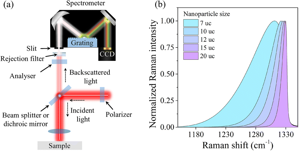 | ||
| Fig. 1 (a) Schematic of a basic Raman scattering setup. (b) An example demonstrating the band shift and band broadening of a Raman signal for diamond nanocrystals54 as a function of number of unit cells (uc) with Raman line shape calculated via a Gaussian confinement approximation (RCF model47,48). | ||
In recent years, with the rapid development of low-dimensional material-based applications, Raman spectroscopy has been used to characterize the size and chemical functionalization of low-dimensional materials such as nanodots, nanowires,44 and two-dimensional (2D) layered materials.45 These low-dimensional materials are particularly interesting in nanophononics due to their ability to confine phonons as they approach length scales in which their finite size or thickness begins to have a strong effect on material properties such as the thermal conductivity.22,46 For example, in the case of nanoparticles, the confinement resulting from the edges of the nanoparticle leads to a break in translational symmetry in the crystal (i.e., absence of periodicity beyond the limits of the particle). This loss of symmetry leads to a shift of the optical Raman modes and an asymmetric broadening of the signal, usually observed as a “shoulder” at lower wavenumber as shown in Fig. 1b. This is induced by the well-known phonon confinement effect. Historically, this effect has been described by a Gaussian confinement model (the Richter–Cambell–Fauchet RCF model),47,48 an elastic49,50 and dielectric51 continuum model, microscopic lattice dynamic calculations for nanoparticles,52 and Density-Functional Perturbation Theory (DFPT).53 The calculation of the line shapes in Fig. 1b were done using the RCF Gaussian confinement model47,48 assuming a spherical Brillouin zone as an approximation for integration, with experimental data for diamond nanocrystals taken from Ager et al.54 More in-depth reviews of how confinement affects Raman modes can be found in.44,55
The finite size of low-dimensional materials is conducive to the activation of forbidden modes56 or the detection of confined acoustic phonon modes.57,58 In general, Raman spectroscopy can only detect zone-center optical phonons (i.e., q = 0). This selection rule is a consequence of the infinite periodicity of a crystal lattice.55 However, in finite-sized systems in which the translational symmetry is broken, the zero-center optical phonon selection rule is relaxed. This causes the Raman spectrum in these finite systems to also have contributions from phonons that are further away from the Brillouin-zone center. This effect can be observed in systems smaller than ∼20 lattice parameters.55 Beyond this limit for larger systems, the contribution of this effect to the Raman spectra is negligible. Acoustic modes (i.e., the natural elastic vibrations of a system) are always present in materials, although they may be difficult to detect. As finite length scales are approached, acoustic modes can begin to be detected. For spherical nanoparticles, their finite size allows for the detection of several discrete Lamb's modes that are associated with spheroidal and torsional modes of the particle.57,59–61 Early demonstrations of detection of phonon confinement using Raman scattering were performed by Colvard et al.62 who measured the folding of longitudinal acoustic phonons in GaAs/AlAs superlattices. They also demonstrated that the phonon folding follows the well-known Rytov equation for infinitely long superlattices,63 a model based on the elastic continuum theory. The first unambiguous demonstration of confinement of optical phonons was measured by Jusserand et al. in 1984, detected using Raman spectroscopy in GaAs/GaAlAs superlattices.49
Confinement in superlattices can be considered to be one-dimensional (1D) since the confinement occurs along the layered axis. Other examples of 1D confinement occur in thin films and van der Waals layered materials. In thin films, confinement of both acoustic58,64 and optical phonons54,55 can be detected. For acoustic modes, the thin film behaves essentially as an acoustic cavity with a wavevector q = nπ/d, where d is the film thickness and n is an integer. For van der Waals materials, the finite number of layers leads to the activation of interlayer modes. These vibrations are associated with an out-of-plane or in-plane displacement of the layers, which are known as breathing modes and shear modes, respectively. Both types of modes are thickness-dependent and are typically used as a fingerprint to determine the number of layers (N) of a van der Waals material.65–68 The thickness dependence of both types of modes can be simulated by using a one-dimensional linear atomic chain model.50,68 This model considers each layer to be a large artificial atom with an effective mass per unit area μ, connected by a spring with an effective interlayer breathing (K⊥) or shear (K‖) force constant per unit area and separated by a distance d given by the interlayer distance. The thickness-dependence of the frequency of the breathing and shear vibrations are given by:
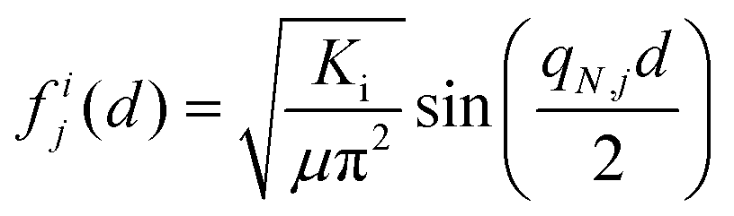 | (1) |
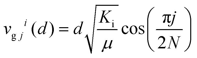 | (2) |
Another interesting property of these modes is that they are also sensitive to the stacking orientation, and the spectral properties of the modes (relative intensities, linewidth, and peak position) can vary as a function of the stacking angle.69–71 These spectral changes are associated with a change in the interlayer coupling strength as well as a change in the crystal symmetry generated by the stacking. This can be observed in Fig. 2, which shows how the Raman spectra changes in a low frequency Raman spectroscopy measurement of bilayer MoS2 for two stacking orientations: A–A (red triangle) and A–B (grey triangles). In another example, Fig. 3 shows a systematic change in the peak position of the breathing mode of bilayer WSe2 films as a function of twist angle.70 It also shows the appearance of the moiré-phonon bands indicated by dashed lines in Fig. 3b.
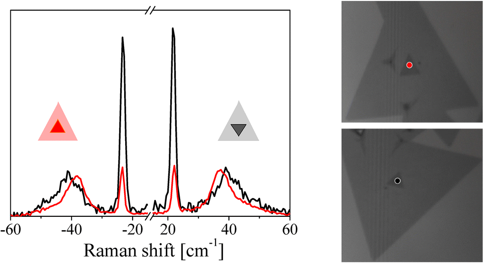 | ||
| Fig. 2 Unpolarized low frequency Raman spectra of MoS2 for A–A and A–B stacking orientations. The measurement was performed using a S&I Raman spectrometer (https://www.s-and-i.de) using a 532 nm wavelength laser with an incident power below 100 μw focused on MoS2 crystals on a SiO2/Si substrate grown via chemical vapour deposition. | ||
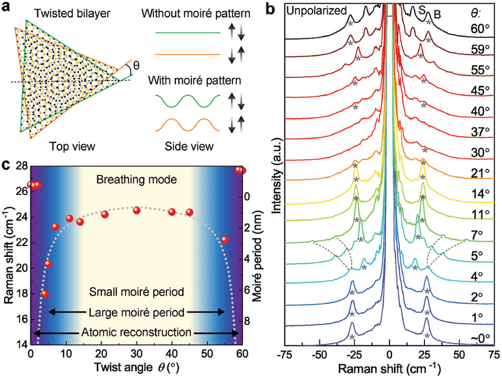 | ||
| Fig. 3 Twist-angle dependence of breathing (B) and shear (S) modes in bi-layer WSe2. (a) Schematic illlustration of the twisted bilayer stacks. (b) Raman spectra for varying stacking angle. Asterisks indicate the interlayer breathing modes and dashed lines indicate the moiré phonons. (c) Peak positions as a function of the stacking angle. Reproduced from ref. 70 with permission from John Wiley and Sons, copyright 2021. | ||
Beyond confinement in these types of 1D systems, two-dimensional (2D) confinement can be observed with Raman spectroscopy in self-assembled molecules (e.g., nanoporous graphene, nanoparticles embedded in a host matrix, or in PnCs), where phonon propagation is restricted to the in-plane direction along the direction of periodicity in the nanostructure. For the case of PnCs, current fabrication techniques are still limited to a minimum pitch of 10's of nm. Since PnCs rely on wave interference, the phonon energy roughly scales inversely with the characteristic length, meaning these pitches correspond to acoustic confinement in the 10–100's of GHz (∼0.3–3 cm−1). Sub-100 GHz frequencies are difficult to measure in Raman spectroscopy, and consequently, the observation of phonons in these types of structures with this technique is limited. Three-dimensional confinement has also been observed in nanoparticles, where the phonon propagation is restricted in all directions.72
Brillouin light scattering
Brillouin light scattering (BLS) spectroscopy is a non-destructive, contactless characterization technique which relies on the interaction of incident light with thermally excited acoustic phonons in a material. The incident light is inelastically scattered by phonons of the sample, modifying the frequency of the scattered light relative to that of the incident light.73 The mechanism is the same as that observed in Raman scattering, with the primary difference being the energy of the phonon involved in the process. Raman scattering generally probes optical phonons in the THz or sub THz range. By contrast, light in BLS is scattered by thermally excited dynamic fluctuations, or MHz–GHz acoustic phonons. These thermal excitations are governed by the equipartition principle of thermodynamics, which states that at a temperature T, a lattice will vibrate randomly with an average amount of energy equal to kBT, where kB is the Boltzmann constant. One advantage of BLS spectroscopy relative to Raman spectroscopy is that for bulk material, it can resolve phonons in the vicinity of the Brillouin zone center, in contrast to Raman which generally can only resolve phonons at the Γ-point.While BLS spectroscopy is usually used in the frequency domain, it can also be resolved in the time domain. Time-domain BLS spectroscopy is a technique that allows for the generation and detection of nanometer-long acoustic pulses using ultrafast, picosecond pulsed lasers to probe the acoustical, optical, and acousto-optical parameters of materials.74 Similarly, pumped BLS spectroscopy combines pulsed photoexcitation at high repetition rates with BLS spectroscopy detection.75 This technique offers a transducer-free source and a detector of spatially confined, standing, and propagating gigahertz acoustic waves, where the photoexcited BLS signal is strongly enhanced compared to that of spontaneous BLS. The main mechanisms that enable the BLS process are the photoelastic76 and moving boundary or ripple77 effects. Both mechanisms are schematically illustrated in Fig. 4. The photoelastic mechanism describes the change in the refractive index of a material caused by strain resulting from propagation of acoustic phonons in the bulk of the material. This mechanism is dominant in transparent materials, and the contribution from the photoelastic effect increases with increasing scattering volume (i.e., material thickness). In these materials, this mechanism is independent of the incident angle of light as only the backscattered light that follows the same path in which it entered is collected. While light is scattered in all directions by the acoustic phonons, the scattered wave is also collected with the same lens that the incident wave entered from. In this case, the mechanical wavevector is always twice that of the incident optical wavevector. It is worth noting that in an anisotropic material, the photoelastic effect can be dependent on the azimuthal angle, as a different crystallographic plane is probed. The photoelastic mechanism is schematically illustrated in Fig. 4a. The phase-matching condition for this mechanism is:
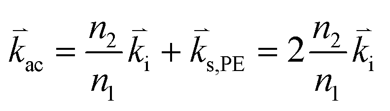 | (3) |
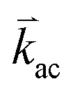 is the resultant photoelastic scattered acoustic wavevector,
 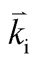 is the incident wavevector,
 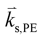 is the photoelastic scattered wavevector inside the material, and n1 and n2 are the refractive indices outside and inside the material, respectively. In Fig. 4a, θ denotes the incident angle and
  denotes the wave reflected by the surface. The moving boundary mechanism, on the other hand, results from dynamic corrugations at the interface, produced by surface displacements. These corrugations act as a moving phase grating that changes the refractive index at the interface and therefore scatters light. This mechanism is dominant in opaque materials and is proportional to the normal displacement of the surface. A larger displacement implies that more light will be scattered at the surface because of the increase in the scattering volume. The moving boundary mechanism is schematically illustrated in Fig. 4b. The inset shows the normal displacement of the moving boundary surface/interface,
  , which is different for each mechanical mode. The phase-matching condition for this mechanism is:
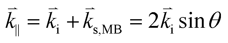 | (4) |
 is the parallel component of the scattered wave and
  is the wavevector of the scattered wave via the moving boundary mechanism. For opaque materials, the normal component of incident light is absorbed by the material, meaning that the conservation of energy and momentum occur via the parallel component of the incident light. In this case, different mechanical
  's from the sample can be probed by changing the incident angle for the phase-matching condition in eqn (4) to be satisfied. This allows for angle-resolved measurements such as experimental mapping or reconstruction of phonon dispersion relations,29,78,79 which generally cannot be done in transparent materials due to the incident angle-independence of the photoelastic mechanism.
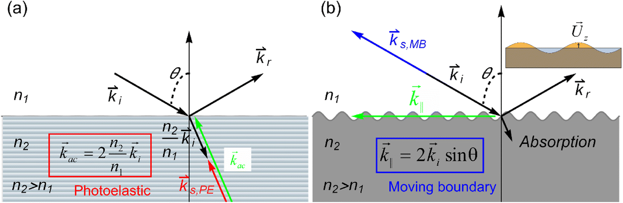 | ||
| Fig. 4 Schematic representation of the (a) photoelastic and (b) moving boundary scattering mechanisms. The inset indicates the normal displacement of the moving boundary surface/interface. | ||
In BLS spectroscopy, as only a small fraction of light is inelastically scattered, the intensity of scattered light is approximately 109 times less than that of an elastically scattered signal and is therefore difficult to detect. In Raman spectroscopy, this problem is solved by incorporating diffraction gratings. However, the several order of magnitude difference in energy between optical (∼10's of THz) and acoustic phonons (GHz) greatly complicates the detection of Brillouin scattered photons. A high contrast spectrometer that is able to achieve high extinction of the elastically scattered light, is required to effectively distinguish BLS signals. This is accomplished with Fabry–Pérot interferometers (FPIs). The spectral resolution of the instrument is defined by the width of the transmitted peak, which depends on the distance over which the mirrors are separated.80 This distance sets the free spectral range, and consequently the spectral resolution that can be obtained with BLS spectroscopy, which is usually on the order of MHz. A single FPI itself does not provide sufficient contrast to detect inelastically scattered light. Two solutions are implemented to circumvent this problem: multi-pass systems, where the light passes multiple times through the same interferometer,80 and a tandem interferometer configuration, where two or more interferometers are placed in series. The additional contrast that is obtained with two FPI in series, which results from an increase in the free spectral range and additional trips through the cavities, is sufficient to detect inelastically scattered light.81 A diagram of this configuration is shown in Fig. 5a. The main disadvantages of such a configuration are the necessity for high spectrometer mechanical stability and the long acquisition times (sometimes days) required for such a measurement.
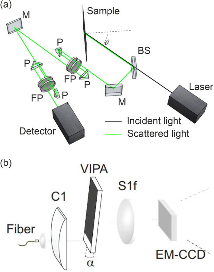 | ||
| Fig. 5 (a) Simplified schematic of a tandem Fabry–Pérot interferometer used to measure and enhance the backscattered signal. BS: beam splitter, M: mirror, P: prism, FP: Fabry–Pérot cavity. (b) Schematic of a single-stage VIPA spectrometer. C1: cylindrical lens, α: angle inclination of VIPA (this inclination is optional, but is sometimes used to increase the contrast of the interferometer), S1f: spherical lens. (b) Reproduced from ref. 84 with permission from Optica publishing group, copyright 2011. | ||
To reduce the acquisition time required using tandem FPIs, confocal microscope systems based on virtually imaged phase array (VIPA) spectrometers have been developed in recent years.82 In these systems (Fig. 5b), the scattered light passes through a VIPA (a solid etalon), producing a spectrally dispersed pattern in the focal plane of the spherical lens that is placed after the VIPA, and the resulting pattern is projected onto a CCD camera.82 As is the case with a single FPI, the main limitation of a single-VIPA spectrometer is the low extinction (or spectral contrast) of the elastic signal. To improve the contrast, two VIPA spectrometers have been orthogonally placed in tandem to one another.83 Additional strategies have been implemented to increase the contrast of this type of spectrometer, such as: placing a third VIPA spectrometer stage,84 using a Fabry–Pérot etalon as a narrowband filter,85 and optimizing signal collection efficiency,86 among others. With the incorporation of VIPA based spectrometers, acquisition time can be drastically reduced down to ∼100 ms, even for low-power incident light, extending the application of this technique to biological materials which are generally more sensitive to damage by light.83 As a consequence, the capacity to measure mechanical properties non-invasively and in vivo at the cellular scale has extended applications of BLS imaging to the realm of biomedicine and biomaterials.83–85
Originally, Brillouin spectroscopy was intended primarily to determine the elastic properties of bulk materials and layered structures.87 Subsequently, it has been deployed to determine elastic properties of materials such as polymers88 or biological systems.89 More recently, this technique has been applied to the investigation of other physical phenomena in diverse materials and structures. One of the main applications of BLS spectroscopy has been the detection of confined modes in a variety of nanostructures such as nanoporous alumina,90 thin films,17,91 nanospheres,31 nanowires,92 nanocubes,93 2D materials,94 and core–shell structures.95 Additionally, there has been growing interest in the use of Brillouin scattering to investigate acoustic phonons in phononic crystals29,30,96 and to detect guided modes in phononic waveguides.78 BLS spectroscopy has also been shown as a promising technique to study and detect theoretically predicted topologically protected phonon states, phonon chirality, and phonons in the hydrodynamic regime.97 At higher incident powers, stimulated BLS can occur, which is an effect that is particularly relevant to consider in optical fibers.98,99
Laser doppler vibrometry
Laser Doppler vibrometry (LDV) is a characterization technique that allows for the contactless measurement of vibrational displacements by detecting the reflected laser beam that experiences a Doppler shift resulting from a moving surface. Interferometric analysis of the backscattered light combined with advanced interferometric (typically heterodyne) detection and signal analysis methods100 are used to quantitatively reconstruct the vibration amplitude and frequency.101 LDV finds applications at various length scales ranging from macroscopic scales (e.g. to perform contactless structural health monitoring of mechanical structures in industry applications102,103 down to the nanoscale where it is used to characterize micro- and nano-mechanical vibrations.104 A general treatment of LDV can be found in other reviews.105,106 Although LDV can be adapted to detect in-plane waves,107 shear waves,107 or torsional motion,108 we limit the scope here to scanning-LDV approaches as it is better suited to the study of on-chip phononic devices. In this case, the optical probing apparatus is coupled to an imaging technique that enables reconstruction of the surface displacement field (schematically illustrated in Fig. 6). Scanning-LDV can be adopted for the detection of any planar waves that display a significant out-of-plane component.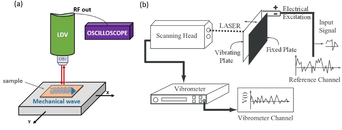 | ||
| Fig. 6 Layout of a typical LDV system. (a) Schematic of scanning-LDV system. (b) Working principle of the LDV: an electrical excitation causes the suspended sample to vibrate. The laser from the interferometer in the scanning head is focused on a sample. A photo detector records the interference of the back scattered light with the reference beam. An output voltage which is proportional to the velocity of the scanned point parallel to the measurement beam is provided by the vibrometer. Finally, the output signal is obtained as velocity or displacement signal using the velocity or the displacement decoder. (b) Reproduced from ref. 121 with permission from IOP Publishing, copyright 2009. | ||
Contactless techniques such as Raman or Brillouin spectroscopy and LDV are essential to sense vibrational motion without altering the local elastic properties while providing access to the natural mechanical properties. Some of the other techniques that are discussed later on in the review can be more invasive. For example, integrated transducers such as interdigitated electrodes or plasmonic resonators introduce dissipation and can perturb the vibration frequency. Moreover, these solutions often cannot be implemented due to application-specific device geometry or material requirements. As such, interferometric optical techniques such as LDV present an advantage in that they allow for remote determination of the mechanical properties of all types of solid state systems, regardless of the material. That being said, the detection requires sufficiently high back-scattered intensity which implies that the surface reflectivity should be reasonably high. It is also worth noting that local changes of the elastic properties at the laser spot position such as changes in the mechanical frequency of a free-standing structure or changes in the reflectivity can also occur with photo-thermal absorptive materials. Standard LDV generally utilizes frequency-domain analysis of the mechanical motion, and can be used to perform a modal analysis of a structure,109 although time-domain studies are also possible for the elucidation of transient dynamics of mechanical motion. LDV time-domain measurements are sensitive enough to be applied even to the detection of thermally excited motion by measuring the noise spectrum of the displacement in the time domain, which provides information regarding the eigenmodes of the system.
Modern scanning-LDV systems fulfil the requirements to investigate nanomechanical motion in most phononic platforms. With sub-picometer displacement sensitivities,110 these systems can be used to sense the out-of-plane displacement induced by the propagation of surface acoustic waves. Commercial scanning-LDV systems are now capable of high-frequency demodulation (i.e. above 2 GHz), which makes this technique particularly attractive for the study of acoustic platforms operating in the GHz frequency range, such as for the characterization of piezoelectric actuators111 or for their combination with suspended nanomechanical waveguides.112 In addition, scanning-LDV provides a singular advantage over other sensing methods by enabling displacement fields to be accurately mapped spatially, both within reasonable acquisition times and with lateral resolution limited essentially by diffraction.113 The displacement field which is acquired point-by-point can be reconstructed over a mechanical oscillation cycle using a reference clock. This contains crucial information that is generally not obtainable with other detection techniques. For example, scanning-LDV facilitates identification of a given mechanical mode with regards to the associated finite-element simulations, which would otherwise be limited to a comparison of the mode's spectral position in experiment versus simulation. It also enables an advanced analysis of the dissipation mechanisms by identification of the loss channels, highlighting the weakness of a given design. Accounting for these loss mechanisms is particularly relevant in the context of topological phononics.114 Scanning the displacement field can also reveal extremely insightful information that is useful to highlight the chirality of a mechanical oscillation on both sides of a topologically protected interface.115,116 Fast mapping experiments enabled by LDV also greatly facilitate the investigation of collective dynamics encountered in nano- and micro-mechanical arrays.117,118
Despite its advantages, LDV is limited to relatively low frequencies compared to other sensing techniques such as cavity optomechanics or Brillouin light scattering. The frequency demodulation of a heterodyne signal remains limited by the laser spot size,113 although recent progress in modal analysis has allowed for an increase in the limit demodulation frequency.119 Furthermore, thermally excited phonon modes generally remain too weak to be accessed by LDV, especially for high frequency systems which exhibit weaker displacements. Therefore, LDV detection must often be accompanied by a separate excitation method such as interdigitated transducers111,112 or other types of actuation.120
Scanning probe microscopy
Surface acoustic waves (SAWs) can be generated by applying an oscillating signal to a suitably designed set of surface gates. While the detection of SAWs most commonly incorporates optical techniques, their application often suffers from limited lateral spatial resolution due to the optical diffraction limit. Furthermore, conventional optical methods are not applicable for subsurface imaging. Acoustic methods122 and non-invasive optical123 and scanning probe microscopy (SPM) based techniques that incorporate a physical probe to scan a surface have been extensively employed for the detection of SAWs. For instance, acoustic techniques such as scanning acoustic microscopy (SAM) provide improved spatial resolution as they use ultrasonic waves with higher frequencies, although the spatial resolution is still limited by the Rayleigh criterion. These techniques have been applied for detecting cracks, voids, and delaminations within micro-devices.124,125 Commercial SAM setups usually operate at frequencies between 10 and 100 MHz.To overcome the diffraction limited resolution in acoustic microscopy, near-field scanning probe techniques have been developed such as scanning near-field ultrasonic holography (SNFUH).126 SNFUH uses ultrasonic plane waves that enter through the bottom of a sample for the characterization of the elastic properties of surfaces as well as of buried structures (or material) in 3D geometries,127 providing a quantitative method for SAW detection. The technique uses an aperture or tip as an antenna, which is brought into close proximity with the sample. The spatial resolution is then determined by the size of the contact area between the antenna and sample. One of the earlier demonstrations of this concept was by Zieniuk and Latuszek,128 who built a scanning near-field acoustic microscope using a pin probe as the antenna, although this was limited to a poor spatial resolution of about 10 μm. Progress in SPM techniques has since yielded higher resolution near-field acoustic imaging. Today, SPM methods incorporate nanometer size tips (∼10 nm), which allow for nanoscale near-field acoustical imaging. The main drawback and difficulty of the detection of ultrasound waves via SPM methods is the limited frequency detection bandwidth, limited by the frequency of the cantilever which ranges from 5 MHz to a few kHz.
Several works have reported similar acoustic imaging instruments based on scanning tunneling microscopy (STM), which takes advantage of quantum tunneling and piezoelectric effects to scan a surface using a conductive metal tip to which a voltage is applied.129–131 In these methods, the surface displacement is monitored either through the tunneling current or through the ultrasonic transmission through the tips. Scanning tunneling acoustic microscopy (STAM), for instance, combines STM with acoustic techniques.132,133 The main principle of STAM is based on the detection of strain-generating interactions. By modulating such an interaction, strain located at the surface near the tip is transformed into an acoustic wave that is transmitted into the sample and subsequently detected by a piezoelectric transducer. The detected acoustic wave provides information regarding the interaction itself, the transmission of the wave, and the elastic properties. Following the invention of STM, Chilla et al. used ultrasonic STM to detect both the out-of-plane and in-plane components of SAWs.134 While STM presents many advantages, its application is limited only to conductive samples.
As an alternative, atomic force microscopy (AFM) has no such limitation, which resulted in significant efforts to realize acoustic imaging with AFM. For example, in atomic force acoustic microscopy (AFAM), a transducer is used as a generator while a scanning probe tip is used as a detector. The generated acoustic wave penetrates through the sample and is subsequently detected by a scanning probe working in the near field. Calculating the amplitude or phase of this wave reveals the acoustic properties or defects of a material.135,136 The resolution in AFAM is wavelength independent, and therefore can be implemented down to the nanoscale even for specimens with thicknesses on the order of hundreds of microns. Many other similar methods for detecting ultrasonic vibrations with an AFM have also been proposed. First, Yamanaka et al.137 developed an AFM-based method to detect ultrasonic vibrations of the sample at frequencies much greater than those of the AFM cantilever resonances. Later, the same group used an ultrasonic force microscope for imaging subsurface defects in graphite with a resolution better than 10 nm.137,138 To date, this technique has been used for nanoscale imaging of structural and mechanical properties of complex nanostructures and thin films.139 Similar ultrasonic AFMs were used for the mechanical mapping of material surfaces.140–142 Furthermore, the detection of ultrasonic surface vibrations with MHz range bandwidth has been accomplished by adding an optical knife-edge detector in an AFM setup.143,144 In addition, AFM based probe systems for the detection of laser-induced SAWs have been reported.145 One of these systems is shown in Fig. 7a. A pulsed laser beam irradiates a surface at point A and induces a SAW which propagates along the surface. The vibration of the surface at point B is then measured by an AFM probe.
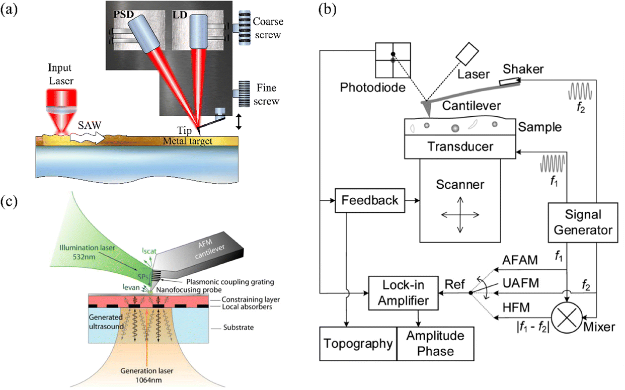 | ||
| Fig. 7 (a) Schematic of an AFM-based probe system for detecting laser induced surface acoustic waves. A photo-sensitive detector (PSD) and laser diode (LD) are indicated. (b) Schematic of an AFAM setup. The vibrations of the cantilever are excited either by a transducer below the sample (transducer 1) or by a transducer which is positioned on the top end of the cantilever (transducer 2). The low frequency components of the beam deflection signal are used to control the static deflection of the cantilever. (c) Schematic of an ultrasonic near-field optical microscopy setup using a plasmonic probe. (b) Reproduced from ref. 151 with permission from AIP Publishing, copyright 2020 and (c) from ref. 149 with permission from AIP Publishing, copyright 2013. | ||
To improve detection sensitivity, the AFM technique must be operated at the resonance frequency of the cantilever in contact with the sample. Consequently, several ultrasonic AFM techniques have been developed based on different excitation and detection schemes for ultrasonic waves such as ultrasonic atomic force microscopy (UAFM)146 and AFAM.147,148 The latter uses ultrasonic waves between the AFM scanner and a sample. The sample is bonded to an external transducer which generates longitudinal ultrasonic waves with a center frequency of several MHz supplied by a function generator. The ultrasonic waves propagate through the sample resulting in out-of-plane vibrations of the sample surface. Those vibrations are monitored via deflections of the AFM cantilever in contact mode operation. To simultaneously extract surface topography along with the acoustic amplitude and phase of the cantilever vibrations, the signals are analyzed with a lock-in amplifier. A schematic of an UAFM technique is shown in Fig. 7b.
Further progress has been achieved with the development of ultrasonic near-field optical microscopes (UNOM) that enable local mapping of ultrasound with deep sub-optical wavelength spatial resolution. As an example, Ahn et al. generated ultrasonic waves with a pulsed laser and detected them with a scanning near-field optical probe over a broad frequency bandwidth (see Fig. 7c).149 They used a plasmonic probe which enhanced the scattering of evanescent light at the probe-tip and enabled reliable measurement of the motion of the surface. Lastly, an AFM-based technique has recently been developed for the imaging of hyperbolic phonon polaritons in two-dimensional (2D) materials,150 demonstrating the potential of SPM methods for characterizing nanomaterials.
Cavity optomechanics
Cavity optomechanics (OM) studies the interaction between light and mechanical motion. Within cavity OM systems, a driving laser couples to mechanical motion via the radiation pressure force where light–matter interactions result from the exchange of momentum between an object and the electromagnetic field. The mechanical motion also modulates the output optical field, which is measured. This interaction is enhanced within an optical resonator. The canonical system for cavity OM is that of an optical cavity created between two mirrors, where one mirror is movable by suspension or by attachment to a spring. Both static and dynamical phenomena arise in this configuration. Firstly, the static displacement of an optomechanical cavity under the radiation-pressure force acts analogously to the Kerr nonlinearity for the optical cavity in that its resonance frequency is power-dependent, which can lead to a bistability.152 Secondly, the mechanical motion which changes the cavity length subsequently also dynamically affects the optical field by shifting the optical resonance frequency. This feedback loop in which the optical and mechanical oscillators act on one another is known as optomechanical backaction. In this manner, cavity OM allows for the control and detection of nanomechanical motion using light. The work done by the radiation pressure can effectively lead to heating (amplification) or cooling (damping) of a mechanical resonator depending on if the driving laser is red or blue detuned relative to the cavity resonance. To maximize efficiency, these processes require that the cavity decay rate is at most on the order of the mechanical frequency which causes the system to enter what is known as a resolved sideband regime. This requirement implies that cavity OM systems are generally designed to maximize their optical quality factor. While cavity OM is a very active and growing area of research, many of the recent breakthroughs in modern optomechanics began with the work by Braginsky,153,154 who studied the measurement of small signals towards the goal of gravitational wave detection. This goal was experimentally demonstrated by LIGO.155 Cavity OM shows significant promise in metrology, sensing, and the study of mechanical systems even down to the quantum level.156–158 Recent advances in the field of cavity OM include the generation of optomechanical entanglement via optomechanical amplification159 and the ability to observe quantum phenomena in mechanical oscillators via ground-state cooling.160–163 There have been many additional examples of OM systems at various length scales to date, and a more general treatment of the basics of cavity OM can be found in other reviews.37,164,165 While the entire field of OM is quite broad, and can in the most general sense be used to describe any system in which mechanics are probed by light, we limit the scope of this section of the review to the detection of mechanical modes solely in on-chip cavity OM crystal systems at the micro/nano-scale, while many of the same ideas are further applicable to cavity OM systems at other length scales as well. It is worth noting that many other exotic systems also exist such as optical tweezers and levitated nanoparticles166–171 or levitated superfluids.172–175Realizing cavity OM at the nanoscale can be difficult, and common systems towards this end include microwave circuits,176 micro/nano-mechanical resonators,177,178 and OM cavities in 1D (e.g. nanobeams)179–187 and 2D (photonic/phononic crystals).188–190 At these scales, these systems sustain mechanical frequencies from the kHz up to the 10's of GHz scale. Recently, some systems have demonstrated resonant mechanical frequencies up to 100 GHz.191 Limitations in fabrication resolution at the nanoscale and detection of these high frequency oscillations prevent the realization of nanoscale OM systems at even greater frequencies. Cavity OM systems enable extremely sensitive readout of mechanical motion, even when the motion is driven by thermal forces. However, the detection of such weak perturbations of the optical field requires the use of appropriate tools. Radiofrequency (RF) photodetectors and electrical spectrum analyzers (ESAs) constitute a common approach to extract this signal, although low-noise amplification of the optical and/or the electrical signal can sometimes be essential to extract these signals from the residual noise of the detectors (e.g. dark noise/shot noise). Interferometric methods, such as homodyne192 or heterodyne detection193,194 can also be implemented to subtract the noise originating from laser fluctuations. Measurements are often frequency-resolved, although time-resolved OM measurements can also be done to study the dynamics of a system. These time-resolved measurements tend to be limited to relatively lower frequency mechanical modes. While the frequency resolution that can be obtained is usually limited by the resolution bandwidth (RBW) of an ESA, this is generally not a limiting factor in cavity OM, as OM resonances are at least on the order of a few 10's of kHz in the lasing regime, or on the order of several MHz in the thermal regime. These systems tend to be limited by the displacement sensitivity (smallest displacement change that can be detected) and the dynamic range (measurement limit due to nonlinearities in the cavity system or electronic limitations of the detection equipment) which compete with one another.195 The displacement sensitivity is limited by the quality factors of the optical resonances within the cavity, and consequently also require extremely narrow-linewidth, low noise lasers. Optical quality factors on the order of 105–106 have been reported in nanoscale cavity OM platforms at room temperature, though much higher quality factors can be reached at cryogenic temperatures.196 Within these systems, displacement sensitivities less than fm/Hz1/2 can be reached, although this limits the dynamic range to a few nanometers.197 The dynamic range is limiting since any mechanical motion of the cavity is detected by tracking the linear part of an optical resonance. The consequence of this is that relatively low optical powers must be used, such that a linearized OM approximation can be used, and any non-linearities (e.g., thermo-optic, free carrier dispersion, or Kerr effects) that affect the linear regime of a cavity optical resonance are avoided. Noise limitations such as dark noise, a generated current due to thermal excitations that is present even in the absence of incident photons, and shot noise, an electronic noise resulting from the discrete flow of charged particles, in any detection readout electronics such as the ESA and photodetectors also must be considered. Even the dynamical back-action is itself a source of noise (radiation pressure shot noise).198 Many of these limitations are not unique only to cavity OM, though they become practically relevant due to the much better displacement sensitivities that can be achieved in cavity OM which are generally much smaller than many other experimental techniques.
OM systems are often engineered to be monomode photonic crystal cavities. Coupling into these guided optical modes of an OM cavity can be complex, often requiring the use of a bus waveguide, grating couplers, or a tapered fiber that enables coupling from free space. Using a tapered fiber from which light can evanescently couple to a cavity enables phonon detection at high spatial resolutions as light can be coupled even to specific individual nanocavities, although this could be considered an invasive probe. Any additional waveguide architectures on the same chip that are coupled to the device of interest could also be considered invasive. Recent work has studied the ability to access and excite mechanics by driving with Anderson-localized optical modes,190,199 while direct experimental evidence of localized mechanical modes still has yet to be demonstrated. Spatial mapping of the mechanics is also possible, following a procedure such as that demonstrated by Ren et al.200 in which a 300 MHz topological channel can be probed by optomechanically interrogating the optical cavities embedded in a lower length scale photonic crystal. In this example, the dissipation occurring at the sharp corners of the acoustic channel allow for a comparison between trivial and topological waveguides.
While OM serves as a powerful tool to detect and control phonons in the kHz–GHz regimes at the micro/nanoscale, OM ideally requires strong confinement (i.e. high quality factors) of both the photons and of the phonons, to increase the quality factors of the optical and mechanical modes while maintaining a small mode volume to enhance photon–phonon interaction and coupling. Within these types of systems, careful consideration of design is required to enable this confinement and utilize OM detection. Fabrication imperfections can lead to the breaking of symmetries and allow coupling between the different phononic symmetries, though this can be overcome by surrounding the OM crystal with a phononic radiation shield that possesses a full phononic gap.180,182 These careful design considerations limit the use of OM techniques for phonon detection to those in which photonic/phononic cavities can be incorporated. However, OM crystals, particularly those based on silicon platforms, are readily incorporated into integrated photonic/phononic circuits due to their compatibility with existing CMOS technologies.
Pump–probe
The invention and widespread adoption of femtosecond (fs) lasers opened the possibility to study non-equilibrium systems with fs resolution dynamics. When a material is illuminated by an ultrashort pulse of light, rapid dynamics are triggered. During this process, a photon–electron interaction occurs. In semiconductor materials, an electron–hole pair is generated.201 In metals, electrons that are within the Fermi energy are excited to higher states, then subsequently diffuse into the sample and transmit their energy to the lattice via electron–phonon interactions.202–204 Thermalization with the ion lattice then follows this photon–electron interaction for both semiconductor and metal materials. This process converts electromagnetic energy into mechanical energy, which produces a photo-induced stress. The relaxation of this stress can launch coherent mechanical vibrations (i.e., coherent acoustic phonons) in a system with frequencies up to 10's of THz.205–208 The different modes and the frequencies at which a system vibrates depend on its shape, composition, and surrounding medium.205,209–213 Generation and characterization of phonons and measurement of the different oscillation mode frequencies is usually done by employing pump–probe techniques. The study of the different mechanical oscillation modes is of fundamental importance as it provides information regarding mode lifetimes (and indirectly the losses within a certain material, the nature of forces between layers in van der Waals materials, and the nature of the adhesion of nanostructures to a substrate, to name a few examples. These techniques generally begin with a single mode-locked laser that is divided into two separate beams. One is the excitation beam (pump) which excites and induces dynamical processes in a sample while the other is the detection beam (probe) with which the state of the sample at any given moment can be detected. During a measurement, they are temporally and gradually delayed from one another, and the transmittance/reflection of the probe is collected. This process is schematically illustrated along with a typical expected optical response in Fig. 8.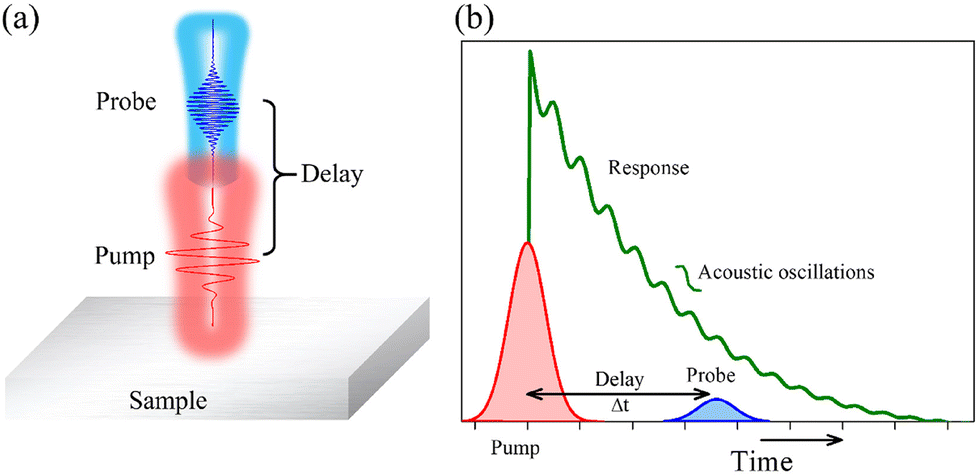 | ||
| Fig. 8 Pump–probe technique. (a) Pump–probe measurement configuration. (b) Typical optical response of a sample under pump–probe excitation. | ||
The incident pump beam used for excitation causes a conversion of optical to mechanical energy, which manifests as stress in a sample (and eventually the generation of a phonon). Consequently, the dielectric properties around the illuminated area undergo periodic perturbations due to the vibrations produced from the stress relaxation. These mechanical oscillations depend on the properties of the material, the surrounding medium, and on the characteristics of the pump pulse, and cause a change in the refractive index due to the volume change associated with a specific excited mode. The affected area of the sample then oscillates at a certain frequency, until it once again reaches mechanical equilibrium. The two main mechanisms by which stress in a solid can be generated following optical excitation are via the deformation potential and thermoelasticity. The dominant mechanism is material dependent, but consideration should also be given to the specific geometry of a system (e.g., thickness), which also plays a role in determining which mechanism contributes a greater effect. The deformation potential mechanism tends to dominate in semiconductor materials, where coherent phonons are generated by a change in the electronic distribution (and hence in the electron–ion and ion–ion interactions). More specifically, the incident laser pulse modifies the carrier distribution, causing some bands to be populated and depopulated. This change in carrier distribution perturbs the lattice configuration equilibrium, notably, without heating the lattice. As the equilibrium position of the lattice is modified, photo-induced mechanical stresses are introduced in the lattice that lead to subsequent generation and emission of a coherent phonon.212,214,215 In the case of the thermoelastic mechanism, which tends to dominate in metals, acoustic coherent phonons are generated due to lattice anharmonicities and the interaction between acoustic and optical modes. Following the incidence of a short light pulse over a metallic surface, light absorption causes electrons within the photon energy of the Fermi surface to be excited,202,216 producing a population of hot electrons that are in non-equilibrium with the lattice.201,214 These hot electrons undergo thermalization via electron–electron electron–phonon interactions, and excitation energy of the electrons is transferred to the lattice through electron–phonon collisions leading to a temperature increase relative to that of the lattice temperature. The increase in lattice temperature and associated thermal expansion cause induced thermoelastic stresses that eventually lead to the generation of phonons.201,202,215–219
Following the dynamics caused by a pump pulse, mechanical vibrations in a material modulate an optical response that can be detected as a change in reflection/transmission of a probe pulse. The oscillatory modification of the dielectric properties produced by the phonons will cause a change in the transmission/reflection of the probe beam in the time domain.212 From these transmission/reflection measurements of the probe beam for different time delays after the pump incidence, the state of a system can be determined at any given moment in time, with each moment determined by the time delay between pump and probe. The dynamics launched by the pump beam can be readily reproduced with a temporal resolution that depends on the delay between pump and probe beams and the width of the laser pulses, which are usually on the order of 10's of fs. The time delay is typically generated after sending the probe beam through a linear translation stage controlled with a stepper motor. For each step of the stage (in units of distance), there will be a temporal separation between the beams that can be calculated after every step by considering the light's velocity. Since the function of the probe is to interrogate the sample, ideally without affecting it in any manner, the power of the probe tends to be an order of magnitude smaller than the pump. The polarization and wavelength of the pump, the probe, or both, can be readily manipulated, as required by the specific phenomena of interest. Additionally, at the moment in which detection occurs, the probe beam must be differentiated from that of the pump. One way to achieve this is with a non-linear crystal, which is commonly placed in the path of one of the beams to modify its wavelength. This allows the beams to be easily separated from one another at the detector using color or interference filters. Other separation methods include separation by polarization or angular separation in which the beams can be filtered spatially. Additional details regarding detection via pump–probe techniques can be found in.218
One state-of-art technique for the generation and detection of coherent phonons in nanostructures is the Asynchronous Optical Sampling spectroscopy (ASOPS).220 The ASOPS method is based on traditional ultra-fast pump–probe techniques, although it produces pulses from two mode-locked lasers with slightly detuned repetition rates rather than incorporating a mechanical delay line for the temporal dephasing of the lasers. ASOPS uses the detuning of the repetition rate between the pump and probe pulses. This detuning creates a monotonic temporal window that allows the dynamics of the system under study to be scanned without requiring any readjustments of the mechanical stage. The scan rate is determined by the difference in frequency, ΔfR, and the temporal window is given by the inverse of this difference, 1/ΔfR. For example, if the repetition rates of the pump and probe are 1 GHz and 0.999999 GHz, respectively, a temporal window of one nanosecond can be probed in 0.1 ms.
One application of the pump–probe technique has been the measurement of coherent phonon modes from which the lifetimes can be extracted and compared with different theoretical models over different frequency regimes.19 Phonon lifetimes are crucial for efficient device performance, as they are closely linked to the quality factor, and therefore to the energy damping time and attenuation factor.19,221,222 For sufficiently long phonon lifetimes and phonon coherence, information can be preserved, allowing for the robust control and storage of information.223 A phonon's lifetime refers to the timescale over which a phonon is scattered or attenuated. The reason for this attenuation can be due to either its collision with impurities or defects within a sample or its boundaries (extrinsic mechanism), or due to the intrinsic anharmonicity of the lattice, which occurs even in perfect crystals (intrinsic mechanism). Together with the group velocity, the phonon lifetime defines how far a phonon can carry its energy, which is known as the phonon mean free path. Despite the fundamental importance of this parameter, accurate measurements of phonon lifetimes are challenging, and their values are unknown in most materials. Although silicon is the most important material for nanoscale devices, there are very few direct measurements of phonon lifetimes in the gigahertz to terahertz range even in this platform.19,224–227 Recently, the phonon lifetime was measured over the entire Brillouin zone in bulk silicon using neutron scattering.228 The chosen technique to model phonon interactions depends largely on the frequency range of interest. One way to visualize the various frequency regimes is as a function of material thickness (e.g., see eqn (1) for layered materials), as different decay processes dominate at different material thicknesses.19,66,226,229 At lower frequencies (thicker materials), phonon–phonon scattering dominates. Conversely, at higher frequencies (thinner materials), surface boundary scattering is dominant.66 The lifetime for the full acoustic range of frequencies can be estimated via Matthiessen's rule,19,66 which treats each scattering process as independent from one another and determines an effective or total lifetime as τ−1Total = τ−1Boundary + τ−1p–p + …. Fig. 9 shows a comparison of phonon lifetimes for a variety of different material systems obtained for silicon membranes19,226 and nanobeams,182 layered PtSe2,230 and MoSe266 over a range of frequencies. For silicon-based materials the total lifetime includes a combination of boundary scattering and phonon–phonon scattering described by the Akhiezer approximation.231 For the case of MoSe2, Soubelet et al. show that the phonon–phonon interaction is better described by the Landau–Rumer approximation.66 The principal difference between the Akhiezer and Landau–Rumer approaches is how the phonon absorption is described. In the Landau–Rumer approach the phonons are described as particles with absorption caused by collisions between them. The calculation is based on quantum mechanical perturbation theory defined by the Fermi golden rule. On the other hand, in the Akhiezer model, the absorbed phonon is treated as a macroscopic strain field in the crystal, causing a shift in the equilibrium distribution of thermal phonons. The system tends to return to equilibrium via phonon–phonon interactions, resulting in a time-dependence of the system's entropy, which leads to phonon mode absorption.
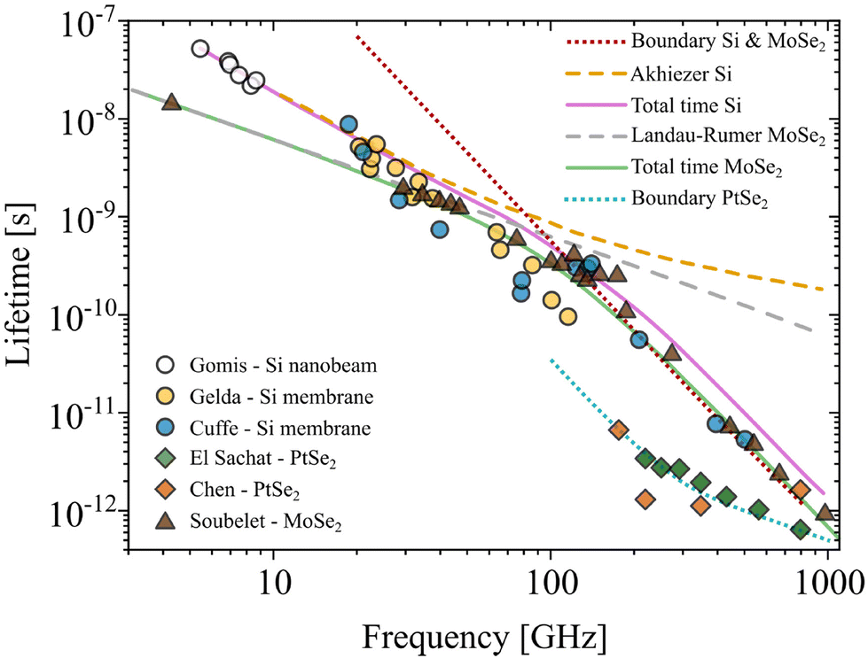 | ||
| Fig. 9 Comparison of the phonon lifetimes as a function of the frequency measured for different material systems compared to the phonon lifetime values as determined by the boundary, Akhiezer, and Landau-Rumer approach for each system. The total lifetime is estimated by Matthiessen's rule. | ||
Beyond phonon lifetimes, the pump–probe technique is versatile with wide-reaching applications and has been used to measure all types of matter from gases and liquids232–234 to solids.205,235,236 Many diverse systems have been characterized such as metallic films,210 acoustic nanocavities,237 piezoelectric materials,238 and 2D materials.209,215,239 The first measurements specifically involving the generation and detection of acoustic phonons by picosecond laser pulses were performed in the 1980s.201,240 The technique was later applied to measure the attenuation of phonons in amorphous SiO2, for frequencies up to 440 GHz.241 Pioneering experimental studies of the detection of confined phonons using a pump–probe technique were performed by Thomsen et al. in 1984.240 They used the modulation of the optical transmission through picosecond pump-and-probe to detect coherent phonons in α-As2Te3 and cis-polyacetylene thin films. Later, Thomsen et al. used the reflected signal to detect confined phonons in α-As2Te3, α-Ge, α-As2Se3, and Ni films.201 Today, this method is widely used to detect confined phonons in many types of nanostructures,212 van der Waals materials,215 and topological superlattices.237 A more exhaustive general analysis of the systems in which coherent acoustic phonons have been studied using the pump–probe technique can be found in other reviews.212,215,236,242,243 For example, Arregui et al. studied the generation of coherent acoustic phonons with frequencies on the order of 100's GHz in topological nanocavities,237 Lin K. et al. demonstrated the generation of acoustic pulses injecting light carriers in piezoelectric materials,238 and Lee et al. and Miao et al. studied the generation and detection of coherent acoustic phonons in black phosphorus.209,239 The generation and propagation of coherent longitudinal acoustic phonons along the cross-plane direction have also been studied in two-dimensional systems, such as organic–inorganic hybrid perovskites,244 van der Waals InSe layered material, and InSe/hBN heterostructures,245 using picosecond ultrasonic pump–probe techniques. Time-domain pump–probe experiments have also enabled the exploration of ultrafast far-from-equilibrium phonon behavior in van der Waals thin films.215,246 In one example, evidence of non-linear lattice dynamics was demonstrated in WTe2 crystals by detecting a large phonon softening with increasing pump power.247 In addition to 2D materials, the resonant vibrational modes and phonon generation and propagation have also been studied in a variety of other nanoscale systems such as nanowires243,248–252 and nanowire arrays, and nanoparticles.204,235,253–256 For example, the coherent generation of longitudinal optical and acoustic phonons in CdTe0.68Se0.32 nanocrystals embedded in glass was demonstrated using femtosecond laser pulses.253
A peculiar case with interesting dynamics arises at the nanoscales in metal nanostructures, where clouds of free electron oscillations known as plasmons can be generated within these structures. If excitation occurs at the resonance frequency of a plasmon, the oscillation amplitude of the electrons can be enhanced. The oscillation frequency and consequently the acoustic phonons that are generated when energy is transferred from hot electrons to the lattice can be controlled by the shape, size, and composition of the specific plasmonic nanostructure.211,242,257–260 These generated mechanical oscillations have shown to be useful for understanding electronic relaxation, sound propagation, and heat management at the nanoscale for sub-diffraction limit dimensions.211 The field of nanoplasmonics, concerned with the study and application of electron oscillations at the metal-dielectric interface of metal nanostructures, has presented unique properties such as nanoscale light confinement and geometrically tunable plasmon resonances, which have been extended into the realm of phonon generation and its associated applications.261–266 For example, coherent acoustic phonons generated by light-induced vibrations in gold nanoantennas have been shown to create propagating surface acoustic waves in the substrate, with the oscillation amplitude and frequency set by the nanoantenna geometry.267,268 In another example, induced coherent acoustic phonons generated via gold nanorods also allow the measurement of the mechanical moduli of polymers at GHz frequencies.269 These represent a few of the many applications in which pump–probe techniques have been incorporated for phonon generation and detection.
Interdigitated transducers
Phonons readily interact with a variety of other quanta, fields, and forces, enabling the realization of devices based on phonon-mediated modulation. However, such devices rely on the emission and detection of traveling phonons, which in most cases tend to require bulky experimental setups such as the techniques described above. To overcome this challenge and leverage these industrially relevant emerging technologies, advanced methods that combine platforms have been recently proposed. These platforms are mainly based on optomechanical interactions, to exploit their technological and functional complementarity. This section provides a brief overview of other remarkable approaches that take advantage of interdigitated electrodes or transducers (IDTs) and surface acoustic waves (SAWs) that lay the foundations for a platform for integrated phononics and photonics.The evolution of IDTs has been constant since their first demonstration in the 60s.270,271 IDTs are metallic comb-like electrode arrays that were traditionally fabricated on a piezoelectric substrate. In this configuration, the piezoelectric properties of the substrate enable electromechanical coupling (i.e., actuation), where a sinusoidal electrical signal on the order of the IDT array period that is applied to the IDT generates a SAW, a surface-localized guided mechanical wave that propagates along the plane of a surface (see Fig. 10a). Conversely, IDTs can also detect a propagating SAW by converting the mechanical wave into an electrical signal.
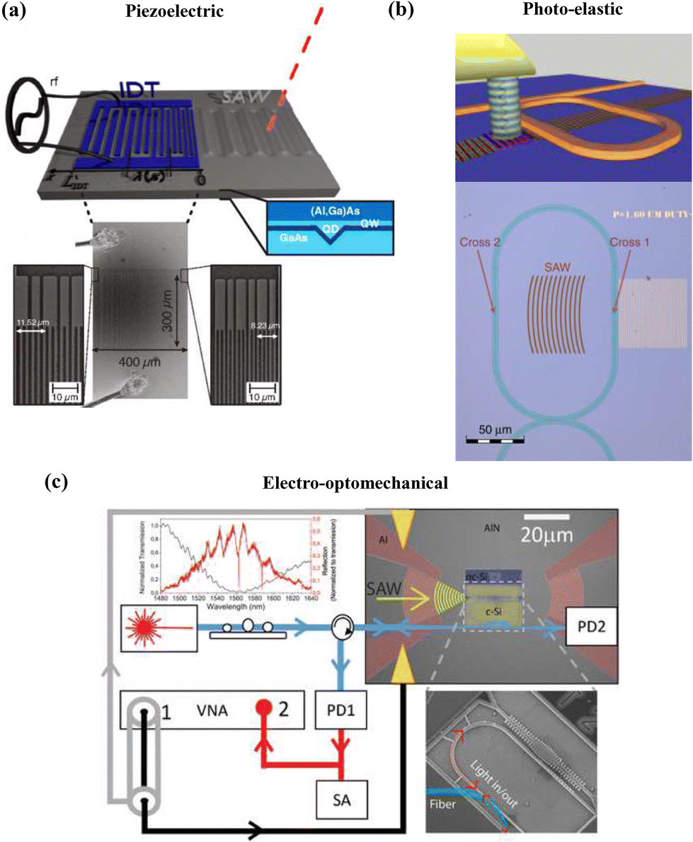 | ||
| Fig. 10 Examples of IDT systems based on: (a) Piezoelectric actuation of acoustic waves; device with metal IDT patterned onto an (Al,Ga)As-based heterostructure (top); SEM images of the IDT (bottom). (b) Photo-elastic coupling; schematic of device where modulated light is absorbed and converted into acoustic waves via thermal expansion of illuminated gold grating (top); optical microscope image of a race-track resonator waveguide and gold grating (bottom). (c) Electro-optomechanical coupling; experimental setup of the nano-electro-optomechanical platform where Al concentric IDTs are used to piezoelectrically launch phonons in a nc-Si optomechanical system which is embedded in photonic circuitry (SEM image, bottom right). (a) reproduced from ref. 298 with permission from American Physical Society, copyright 2017, (b) from ref. 293 with permission from Springer Nature, copyright 2019, and (c) from ref. 295 with permission from American Chemical Society, copyright 2022. | ||
Even many decades following their inception, IDTs and SAWs continue to see widespread application. The potential realization of many types of physical sensors using IDTs has led to an explosion of their use in modern mainstream technologies.270,272–280 In more recent years, improved nanofabrication techniques have resulted in the development of high frequency IDTs operating up to the GHz regime.281–283 Fundamental research has exploited the ability to generate phonons from a RF signal as well as read them out with excellent sensitivities,284–286 and has used them to interact with a wide range of different systems such as optomechanical systems,284 nitrogen-vacancy centers,285 and superconducting qubits.287–289 IDTs have been also employed to manipulate the optical properties of 2D semiconductors by acting as an external stimulus and introducing dynamic 2D lateral modulation of the electronic band structures in 2D materials. In one instance, Rezk et al.290 used SAWs generated by an IDT to effectively modulate the photoluminescence (PL) in quasi-2D MoS2, demonstrating that spatial manipulation of the electroacoustic field associated with the SAW leads to alterations in the excitonic PL. More recently, Scolfaro et al. used the in-plane piezoelectric field carried by SAWs to manipulate charged exciton emission energies and recombination rates in MoSe2 and MoS2 multilayers on LiNbO3 substrates.291
The wide variety of IDT designs (see Fig. 10) make the category of IDTs very peculiar when compared to the other techniques that are discussed within this review. Generally, IDTs operate from the kHz regime up to ∼10's of GHz.283 The exact characteristics (e.g., frequency and spatial resolution, frequency range, bandwidth, signal shape, etc.) that can be obtained are highly dependent on the specific IDT design.292 For example, bandwidth is dependent on the number of digits in the IDT, where more digits result in a more intense signal but a narrower bandwidth. The frequency resolution is a practical limitation, dependent on the experimental equipment available. There are additional considerations when incorporating IDTs that may limit their application, such as the invasiveness of their integration into the underlying sample.
While the field of SAWs generated via IDTs in piezoelectric materials is quite a developed field that has resulted in a plethora of applications,270,273 the electromechanical coupling that is dependent on the requirement of a piezoelectric material substrate can be a limiting factor in many applications. Notably, the lack of CMOS compatibility impedes monolithic integration with electronics. These ideas have already been extended to the realm of photonics, where existing platforms in standard silicon-on-insulator (SOI) have demonstrated simultaneous support of optical and acoustic signals with the goal of on-chip acousto-optic signal processing. Recently, Munk et al. proposed a surface acoustic wave-photonic device fabricated on SOI, completely foregoing a piezoelectric substrate, and operating at frequencies up to 8 GHz (Fig. 10b).293 The photonic device uses surface waves that are launched through the thermal absorption of a modulated optical pump pulse (1540 nm) in a gold grating IDT. The resulting strain from thermoelastic expansion and contraction of the grating is transferred to the underlying silicon device layer, which in turn, can excite a surface acoustic mode of the SOI layer stack. Detection of the surface acoustic waves is based on the photo-elastic modulation of an optical probe in standard race-track resonators. They demonstrate that this photonic device can serve as a discrete-time microwave-photonic filter based on acoustics, with high relevance to signal processing applications. Based on a photonic–phononic emit–receive process, Kittlaus et al.294 proposed a RF filter that uses high-Q phononic signal processing. The architecture is based on an all-silicon photonic–phononic emitter-receiver that exhibits high-fidelity narrow-band filtering (5 MHz) and has the advantage of using a single intensity modulator to encode RF signals onto light. Such a device converts intensity-modulated light in the emit waveguide into phase-modulated light (probe) in the receive waveguide. This is achieved through a linear acousto-optic scattering process mediated by a resonant Lamb-like acoustic mode within a silicon membrane. The probe light signal is filtered through the phononic response of the device (via the acoustic wave generated by the pump) and encoded onto the probe wave by the resulting phase modulation. This device exhibits record-high modulation efficiency compared to state-of-the-art phononic emit-receive devices and exhibits robust performance as a RF-photonic filter.
Other platforms aim to gather together electromechanical or piezoelectrical actuation and optomechanical systems. These electro-optomechanical platforms represent another way of integrating photonics and phononics on a chip. The following examples are potentially straightforward to integrate onto a chip, though they also support electrical actuation, in addition to optical and mechanical signals. Recently, a proof-of-principle technology platform was proposed by Navarro-Urrios et al. (Fig. 10c).295 This platform consists of a nanoelectro-opto-mechanical system that supports the coexistence of electrical, mechanical, and optical signals on a chip. Aluminum IDTs on an aluminium nitride layer generate coherent mechanical waves (2 GHz) that interact with the optical fields confined in nanocrystaline silicon optomechanical nanobeam cavities. The surface acoustic waves generated by the IDTs are converted into guided mechanical waves supported by the nanobeam. At cavity resonance, these mechanical waves strongly interact with the confined optical waves in the released nanobeam OM cavity, enabling microwave radiofrequency-to-optical conversion at room temperature, with a peak sensitivity below 3 phonons. Mayor et al., recently proposed a mechanical waveguide of LiNbO3 (LN) on sapphire (LISA) in an attempt to combine electrical, mechanical, and optical signals altogether onto a single platform, to achieve efficient electromechanical wave transduction for phononic circuits.296 This waveguide combines the high piezoelectric coupling coefficient of LN with the confinement of the mechanical wave achieved through index guiding, due to the slower propagation in LN relative to that in sapphire. The higher refractive index of LN (≈2.2) compared to sapphire (≈1.7) also allows for simultaneous optical guiding within the same waveguide. The evanescent mode profile in the sapphire substrate enables coupling between adjacent waveguides. With this platform, mechanical waves at ≈3.23 GHz are efficiently excited by Al IDTs and guided through the LN ridge waveguide, at room temperature. Delay lines, racetrack resonators, and meander line waveguides are all demonstrated in the proposed platform. Furthermore, this platform has the advantage of being “unreleased” in that the device layer is not suspended, which facilitates its fabrication, scalability, and integration with other photonic circuits. The lack of suspension allows for more ready incorporation with existing CMOS technologies and greatly simplifies the fabrication of dense monolithic all-in-one photonic and phononic circuits.296,297
These advances in complex electro- and piezo-optomechanical circuits show promising avenues for optimal information transmission using multi-state variables in a single chip. Beyond this, they can find applications in integrated microwave photonics, microwave quantum technologies at cryogenic temperatures, and in general, quantum and classical phononic circuits and systems. The rich and diverse physical phenomena that manifest in these electro- and piezo-optomechanical devices may draw a new technological frontier with capabilities beyond the reach of current technologies.
Summary/conclusions
The field of nanophononics is an active and growing field of research, as demonstrated by the many examples provided here. Phonons themselves play a fundamental role throughout various scientific processes, and a complete understanding of their mechanisms and effects is required to realize next generation applications. With the recent advancements in nanofabrication technologies, the limiting factor in further advancement of the field of phononics is largely practical, due to challenges associated with the excitation and detection of phonons or vibrations. Here, we focused on highlighting seven of the available techniques for manipulating acoustic phonons, and provided an overview of the advantages, disadvantages, considerations, and general development of these techniques, which are summarized in Table 1. Cavity OM and IDTs are a particular case among these techniques, in that they require specific nano-architecture on the substrate to enable their incorporation, unlike the other techniques which allow for direct measurement. We define the incorporation of any additional on-chip architecture or physical probe as “invasive”. In this table, the type of modes that can be detected (bulk/surface), bulk refers to modes within the material that are not surface waves, including in the case of low-dimensional materials.| Experimental technique | Frequency range | Frequency resolution | Spatial resolution | Time/frequency resolved | Spatial mapping | Invasive | Bulk/surface | Additional considerations |
|---|---|---|---|---|---|---|---|---|
| a Dependent on laser wavelength, spectrometer focal length, and grooves per mm in the grating. b OM systems are generally limited not by frequency resolution, but rather by displacement sensitivity and dynamic range which compete with one another. c Frequency resolution depends on the experimental equipment available. Bandwidth is set by number of IDT digits. | ||||||||
| Raman | 3–4000 cm−1 (0.089–119.9 THz) | 0.5 cm−1 (14.98 GHz)a | Optically limited (λ/2) | Yes/Yes | Yes | No | Both | Requires Raman active mode |
| BLS | 0.1–1200 GHz | MHz | Optically limited (λ/2) | Yes/Yes | Yes | No | Both | Long acquisition times (∼days) |
| LDV | DC (kHz)–2.5 GHz | Few kHz | Optically limited (λ/2) | Yes/Yes | Yes | No | Surface | Detection of out-of-plane motion |
| SPM | 10 kHz–100 MHz | A few kHz | <10 nm | Yes (∼μs)/Yes | Yes | Yes | Both (mainly surface) | Differentiate the contribution to contrast by surface versus sub-surface material properties |
| Cavity OM | kHz–10's of GHz | kHzb | — | Yes/Yes | No | Yes | Both (indistinguishable) | Designs limited to sufficiently strong OM cavities |
| Pump–Probe | GHz–THz | 10's of MHz | Optically limited (λ/2) | Yes/No | Yes | No | Both | — |
| IDTs | kHz–10's of GHz | Design-dependentc | — | Yes/Yes | No | Yes | Surface | Design-dependent; requires piezoelectric material; can also generate acoustic waves |
Emerging directions
The experimental techniques described in this review have been developed and optimized over time and have resulted in significant progress towards furthering the understanding of phonon behavior. Their continued development will lead to further improvements in temporal and spatial resolution, and consequently provide further insights into the interactions of phonons with other quanta, fields, and forces. Advances in nanotechnology will continue enabling more compact techniques for phonon generation, detection, and control, which serve as a step towards the full integration of phonon sources, waveguides, cavities, and detectors with existing electronic and photonic devices on a single chip. One promising avenue of research that could take advantage of these developments is information and communication technologies (e.g. quantum information, signal processing, etc.).Up until now, platforms exploiting phonon-mediated modulation of optical fields based on photo-acoustic interactions have found applications in acousto-optic signal processing. Numerous devices for tunable optical filtering or wavelength conversion have been demonstrated.299–304 Beyond this, more complex platforms that integrate multi-state variables onto a single chip using electro- and piezo-optomechanical circuits that operate at telecom wavelengths pave the way for optimal information processing and optical communications.295–297 Integrated microwave photonics, microwave quantum technologies at cryogenic temperatures, and in general, quantum and classical phononic circuits and systems are just a few examples of the wide variety of applications that could benefit from the rapid development of the field of nanophononics.
Another emerging direction in early stages of development that is directly relevant to information technologies is topological phononics. Following the recent landmark development of Dirac acoustic materials, the field of topological phononics has garnered a significant amount of additional attention due to its potential to overcome the problem of disorder and perturbation-related losses. Since the pioneering work on the engineering of the acoustic band structure through a two-dimensional periodic array,305–307 PnCs have become a rich and emerging research field. The precise tuning of the dispersion relation has allowed for the observation of exotic phenomena far beyond those found in nature. For example, Dirac cones can be generated by simply tuning lattice symmetry and fill factor.308–311 The Dirac cone manifests as a crossed linear dispersion relation at a point in reciprocal space and is highly robust even under disorder and perturbations. Dirac materials are described by a massless Dirac-like equation and their discovery is considered to be one of the great achievements of condensed matter in the last century. Along these lines, acoustic or phonon topology has recently attracted significant scientific attention. In contrast with topological electronic materials, acoustic topology does not depend on the atomic arrangement of materials. Rather, its properties and manipulation depend only on geometrical parameters, greatly reducing the difficulty associated with the fabrication of structures that exhibit phononic topology.
Xia et al.311 showed that small variations of the geometric parameters can shift the position of the Dirac point without opening it. A break in the mirror symmetry of the geometry can open the dispersion at the Dirac point, yielding directional or complete acoustic band gaps. Lu et al. predicted312 and later demonstrated313 the creation of acoustic vortices in a 2D waveguide via rotational symmetry of a crystal. Using a hexagonal array of triangular rods, Lu demonstrated the existence of an acoustic analogue of the quantum valley-Hall effect. Complementary observations were reported by Yan et al.314 adopting a similar structure, where an array of triangles was fabricated on a silicon chip using CMOS microfabrication techniques. Other unusual properties have also been observed by concatenating two or more lattices with different symmetry, e.g., acoustic pseudospin,315–318 and by a smooth breaking of the symmetry such as is in the case of acoustic pseudomagnetic fields.319
Until now, efforts in topological phononics have generally been limited to low-frequencies (0.1–100 kHz) in rather bulky (10−2–10−3 m) structures.320–322 GHz applications have been demonstrated in one dimensional multilayer systems237,323 while two dimensional systems have been mainly limited to theory.319,324,325 Nevertheless, as the acoustic problems are scale-invariant, sooner or later, macroscopic phononic crystals will be replicated at the nanoscale. At the nanoscale, the principal existing challenge is the selective excitation and detection of acoustic waves that possess these special aforementioned properties. Towards this goal, Brendel et al.319 suggested the use of the radiation pressure in an optomechanical cavity. In this configuration, it is relatively simple to change and control the optical power that couples into the optomechanical cavity. The radiation pressure can then be carefully controlled such that the desired acoustic waves can be effectively generated and launched. Later, the readout can be measured by detecting the sidebands of the reflected laser beam used to excite the acoustic wave. Another possibility is the use of IDTs as “acoustic wave launchers”.326 This platform consists of two IDTs coupled to an acoustic waveguide. One of the IDTs focuses the acoustic power at one end of the waveguide (emitter) while the second one is positioned at the other end of the waveguide (receiver). This particular arrangement could allow for the generation and detection of acoustic phonons travelling through a topologically protected waveguide.327 Simply by reversing the emitter-receiver configuration, it is possible to demonstrate the unidirectionality of a topologically protected acoustic waveguide.
Several scientific advancements have shown the increasing relevance of phononics for information and communication technologies (ICTs) such as resonant acoustic nanocavities, surface phonon polariton lasers, micro-/nano-electromechanical devices, and non-diffusive thermal transport, all of which open the way for manipulating phonons as information carriers. The concept of topologically protected states has enormous potential for information and communication technology as these states can transport energy without dissipation. Similarly, the acoustic version of a topological insulator will allow for phonon transport along surface or edges but not within the bulk. A topological phonon is also immune to scattering by defects and other perturbations (i.e., they can travel along a surface without backscattering). Such technology could enable a platform for robust waveguides, improved acoustic-based devices (e.g., mobile phone sensors, touchscreen, gas, mass and pressure sensors among others), and radio (RF) and intermediate frequency (IF) filters.328 The use of phonons as information carriers opens the possibility of low power computation processes, which would help to reduce energy consumption. Much more generally, robust control over phonon coherence, dynamics, and mean free path promises access to the tunability of all material properties that are dependent on the phonon physics that we have mentioned throughout this review.
Author contributions
R.C.N. and E.C.-A. designed, reviewed, and edited the entire manuscript; R.C.N. wrote and edited the OM section; A.E.S. wrote and edited the AFM section; F.C., O.F., and M.S. wrote and edited the BLS section; G.M. wrote and edited the LDV-based section; M.P., E.C.-A., R.C.N., and A.E.S. wrote and edited the P&P-based section; J.J.F., R.C.N., and G.M., wrote and edited the IDT section; P.X. and E.C.-A. wrote and edited the Raman section; Resources and funding acquisition C.M.S.T.; R.C.N., A.E.S., C.M.S.T., and E.C.-A supervised the work. All authors have read and agreed to the published version of the manuscript.Conflicts of interest
The authors declare no conflict of interest.Acknowledgements
We acknowledge the support from the project LEIT funded by the European Research Council, H2020 Grant Agreement No. 885689. ICN2 authors thank the Severo Ochoa (Spanish Research Agency AEI, grant no. SEV-2017-0706) and the CERCA Programme / Generalitat de Catalunya. R. C. N. acknowledges funding from the EU-H2020 Research and Innovation Programme under the Marie Sklodowska Curie Individual Fellowship (Grant No. 897148). A. E. S. acknowledges support by the H2020-MSCA-IF project THERMIC-GA No. 101029727. F. C. acknowledges funding from the scholarship BES-2016-077203 funded by MCIN/AEI/10.13038/501100011033 and by “ESF Investing in your future”. O. F. is supported by BIST PhD fellowship Horizon 2020 Research and Innovation Programme under the Marie Sklodowska-Curie Grant Agreement No. 754558. P. X. additionally acknowledges support by a Ph.D. fellowship from the EU Marie Skłodowska-Curie COFUND PREBIST project (Grant No. 754558). We would also like to acknowledge the reviewers for this work, who we feel went above and beyond in providing constructive criticism that helped to greatly improve the clarity of this review.References
- L. Rayleigh, Proc. London Math. Soc., 1885, s1–17, 4–11 CrossRef.
- R. Stoneley, Proc. R. Soc. A, 1924, 106, 416–428 Search PubMed.
- A. E. H. Love, Some Problems of Geodynamics: Being an Essay to which the Adams Prize in the University of Cambridge was Adjudged in 1911, Cambridge University Press, Cambridge, 1967 Search PubMed.
- K. Sezawa, Bull. Earthquake Res. Inst., Univ. Tokyo, 1927, 3, 1–18 Search PubMed.
- P. Delsing, A. N. Cleland, M. J. A. Schuetz, J. Knörzer, G. Giedke, J. I. Cirac, K. Srinivasan, M. Wu, K. C. Balram, C. Bäuerle, T. Meunier, C. J. B. Ford, P. V. Santos, E. Cerda-Méndez, H. Wang, H. J. Krenner, E. D. S. Nysten, M. Weiß, G. R. Nash, L. Thevenard, C. Gourdon, P. Rovillain, M. Marangolo, J.-Y. Duquesne, G. Fischerauer, W. Ruile, A. Reiner, B. Paschke, D. Denysenko, D. Volkmer, A. Wixforth, H. Bruus, M. Wiklund, J. Reboud, J. M. Cooper, Y. Fu, M. S. Brugger, F. Rehfeldt and C. Westerhausen, J. Phys. D: Appl. Phys., 2019, 52, 353001 CrossRef CAS.
- L. Pochhammer, J. fur Reine Angew. Math., 1876, 1876, 324–336 Search PubMed.
- C. Chree, Q. J. Pure Appl. Math., 1886, 21, 287–298 Search PubMed.
- H. Lamb, Proc. London Math. Soc., 1881, s1–13, 189–212 CrossRef.
- H. Lamb, Proc. R. Soc. A, 1917, 93, 114–128 Search PubMed.
- M. A. Stroscio and M. Dutta, Phonons in Nanostructures, Cambridge University Press, 2001 Search PubMed.
- P. Maioli, T. Stoll, H. E. Sauceda, I. Valencia, A. Demessence, F. Bertorelle, A. Crut, F. Vallée, I. L. Garzón, G. Cerullo and N. Del Fatti, Nano Lett., 2018, 18, 6842–6849 CrossRef CAS PubMed.
- J. M. Ziman, Electrons and Phonons. The theory of transport phenomena in solids, Oxford University Press, USA, New York, 1960 Search PubMed.
- C. Kittel, Introduction to Solid State Physics, Wiley, 2004 Search PubMed.
- N. Bannov, V. Aristov, V. Mitin and M. A. Stroscio, Phys. Rev. B: Condens. Matter Mater. Phys., 1995, 51, 9930–9942 CrossRef CAS.
- A. A. Balandin and K. L. Wang, J. Appl. Phys., 1998, 84, 6149 CrossRef CAS.
- M.-J. Huang, T.-M. Chang, C.-K. Liu and C.-K. Yu, Int. J. Heat Mass Transfer, 2008, 51, 4470–4479 CrossRef CAS.
- J. Cuffe, E. Chávez, A. Shchepetov, P.-O. Chapuis, E. H. El Boudouti, F. Alzina, T. Kehoe, J. Gomis-Bresco, D. Dudek, Y. Pennec, B. Djafari-Rouhani, M. Prunnila, J. Ahopelto and C. M. Sotomayor Torres, Nano Lett., 2012, 12, 3569–3573 CrossRef CAS.
- E. Chávez, J. Cuffe, F. Alzina and C. M. Sotomayor Torres, J. Phys.: Conf. Ser., 2012, 395, 012105 CrossRef.
- J. Cuffe, O. Ristow, E. Chávez, A. Shchepetov, P.-O. Chapuis, F. Alzina, M. Hettich, M. Prunnila, J. Ahopelto, T. Dekorsy and C. M. Sotomayor Torres, Phys. Rev. Lett., 2013, 110, 095503 CrossRef CAS PubMed.
- N. W. Ashcroft and N. D. Mermin, Solid State Physics, Saunders College Publishing, 1976 Search PubMed.
- G. Agrawal, Nonlinear Fiber Optics, Academic Press, New York, 2001 Search PubMed.
- P. Xiao, E. Chavez-Angel, S. Chaitoglou, M. Sledzinska, A. Dimoulas, C. M. Sotomayor Torres and A. El Sachat, Nano Lett., 2021, 21, 9172–9179 CrossRef CAS PubMed.
- B. Graczykowski, A. El Sachat, J. S. Reparaz, M. Sledzinska, M. R. Wagner, E. Chavez-Angel, Y. Wu, S. Volz, Y. Wu, F. Alzina and C. M. Sotomayor Torres, Nat. Commun., 2017, 8, 415 CrossRef CAS PubMed.
- M. R. Wagner, B. Graczykowski, J. S. Reparaz, A. El Sachat, M. Sledzinska, F. Alzina and C. M. Sotomayor Torres, Nano Lett., 2016, 16, 5661–5668 CrossRef CAS.
- M. Maldovan, Nat. Mater., 2015, 14, 667–674 CrossRef CAS PubMed.
- J. Mendoza and G. Chen, Nano Lett., 2016, 16, 7616–7620 CrossRef CAS.
- M. N. Luckyanova, J. Mendoza, H. Lu, B. Song, S. Huang, J. Zhou, M. Li, Y. Dong, H. Zhou, J. Garlow, L. Wu, B. J. Kirby, A. J. Grutter, A. A. Puretzky, Y. Zhu, M. S. Dresselhaus, A. Gossard and G. Chen, Sci. Adv., 2018, 4, eaat9460 CrossRef CAS PubMed.
- V. Narayanaamurti, Science, 1981, 213, 717–723 CrossRef CAS PubMed.
- B. Graczykowski, M. Sledzinska, F. Alzina, J. Gomis-Bresco, J. S. Reparaz, M. R. Wagner and C. M. Sotomayor Torres, Phys. Rev. B: Condens. Matter Mater. Phys., 2015, 91, 075414 CrossRef.
- M. Sledzinska, B. Graczykowski, J. Maire, E. Chavez-Angel, C. M. Sotomayor-Torres and F. Alzina, Adv. Funct. Mater., 2020, 30, 1904434 CrossRef CAS.
- M. H. Kuok, H. S. Lim, S. C. Ng, N. N. Liu and Z. K. Wang, Phys. Rev. Lett., 2003, 90, 255502 CrossRef CAS PubMed.
- K. Aryana, J. B. Stahley, N. Parvez, K. Kim and M. B. Zanjani, Adv. Theory Simul., 2019, 2, 1800198 CrossRef.
- A. El Sachat, F. Alzina, C. M. Sotomayor Torres and E. Chavez-Angel, Nanomaterials, 2021, 11, 175 CrossRef CAS PubMed.
- A. A. Balandin, J. Nanosci. Nanotechnol., 2005, 5, 1015–1022 CrossRef CAS.
- M. Maldovan, Phys. Rev. Lett., 2013, 110, 025902 CrossRef PubMed.
- M. Maldovan, Nature, 2013, 503, 209–217 CrossRef CAS PubMed.
- A. H. Safavi-Naeini, D. Van Thourhout, R. Baets, R. Van Laer, D. Van Thourhout, R. Baets and R. Van Laer, Optica, 2019, 6, 410 CrossRef.
- J. Cunha, T.-L. Guo, G. Della Valle, A. N. Koya, R. P. Zaccaria and A. Alabastri, Adv. Opt. Mater., 2020, 8, 2001225 CrossRef CAS.
- S. Dzsaber, M. Negyedi, B. Bernáth, B. Gyüre, T. Fehér, C. Kramberger, T. Pichler and F. Simon, J. Raman Spectrosc., 2015, 46, 327–332 CrossRef CAS.
- T. Satoshi, R. Sanford, T. Takao, C. Mahito, T. Tetsuya and T. Tahei, Science, 2008, 322, 1073–1077 CrossRef PubMed.
- P. Kukura, D. W. McCamant, S. Yoon, D. B. Wandschneider and R. A. Mathies, Science, 2005, 310, 1006–1009 CrossRef CAS PubMed.
- D. Heiman, R. W. Hellwarth, M. D. Levenson and G. Martin, Phys. Rev. Lett., 1976, 36, 189–192 CrossRef CAS.
- A. M. Zheltikov, J. Raman Spectrosc., 2000, 31, 653–667 CrossRef CAS.
- M. Ivanda, K. Furić, S. Musić, M. Ristić, M. Gotić, D. Ristić, A. M. Tonejc, I. Djerdj, M. Mattarelli, M. Montagna, F. Rossi, M. Ferrari, A. Chiasera, Y. Jestin, G. C. Righini, W. Kiefer and R. R. Gonçalves, J. Raman Spectrosc., 2007, 38, 647–659 CrossRef CAS.
- P. Vecera, J. C. Chacón-Torres, T. Pichler, S. Reich, H. R. Soni, A. Görling, K. Edelthalhammer, H. Peterlik, F. Hauke and A. Hirsch, Nat. Commun., 2017, 8, 15192 CrossRef CAS PubMed.
- T. Lin, X. Cong, M.-L. Lin, X.-L. Liu and P.-H. Tan, Nanoscale, 2018, 10, 8704–8711 RSC.
- H. Richter, Z. P. Wang and L. Ley, Solid State Commun., 1981, 39, 625–629 CrossRef CAS.
- I. H. Campbell and P. M. Fauchet, Solid State Commun., 1986, 58, 739–741 CrossRef CAS.
- B. Jusserand, D. Paquet and A. Regreny, Phys. Rev. B: Condens. Matter Mater. Phys., 1984, 30, 6245–6247 CrossRef CAS.
- N. S. Luo, P. Ruggerone and J. P. Toennies, Phys. Rev. B: Condens. Matter Mater. Phys., 1996, 54, 5051–5063 CrossRef CAS.
- K. Huang and B. Zhu, Phys. Rev. B: Condens. Matter Mater. Phys., 1988, 38, 13377–13386 CrossRef.
- J. Zi, K. Zhang and X. Xie, Phys. Rev. B: Condens. Matter Mater. Phys., 1997, 55, 9263–9266 CrossRef CAS.
- V. Davydov, E. M. Roginskii, Y. Kitaev, A. Smirnov, I. Eliseyev, E. Zavarin, W. Lundin, D. Nechaev, V. Jmerik, M. Smirnov, M. Pristovsek and T. Shubina, Nanomaterials, 2021, 11, 2396 CrossRef CAS PubMed.
- J. W. Ager, D. K. Veirs and G. M. Rosenblatt, Phys. Rev. B: Condens. Matter Mater. Phys., 1991, 43, 6491–6499 CrossRef CAS PubMed.
- A. K. Arora, M. Rajalakshmi, T. R. Ravindran and V. Sivasubramanian, J. Raman Spectrosc., 2007, 38, 604–617 CrossRef CAS.
- A. Sirenko, I. Akimov, J. Fox, A. Clark, H.-C. Li, W. Si and X. Xi, Phys. Rev. Lett., 1999, 82, 4500–4503 CrossRef CAS.
- M. Fujii, Y. Kanzawa, S. Hayashi and K. Yamamoto, Phys. Rev. B: Condens. Matter Mater. Phys., 1996, 54, R8373–R8376 CrossRef CAS PubMed.
- C. M. Sotomayor Torres, A. Zwick, F. Poinsotte, J. Groenen, M. Prunnila, J. Ahopelto, A. Mlayah and V. Paillard, Phys. Status Solidi, 2004, 1, 2609–2612 CrossRef.
- H. K. Yadav, V. Gupta, K. Sreenivas, S. P. Singh, B. Sundarakannan and R. S. Katiyar, Phys. Rev. Lett., 2006, 97, 085502 CrossRef PubMed.
- A. Girard, J. Lermé, H. Gehan, J. Margueritat and A. Mermet, J. Chem. Phys., 2017, 146, 194201 CrossRef CAS.
- M. Ikezawa, T. Okuno, Y. Masumoto and A. A. Lipovskii, Phys. Rev. B: Condens. Matter Mater. Phys., 2001, 64, 201315 CrossRef.
- C. Colvard, R. Merlin, M. V. Klein and A. C. Gossard, Phys. Rev. Lett., 1980, 45, 298–301 CrossRef CAS.
- S. M. Rytov, Sov. Phys. JETP, 1956, 2, 466–476 Search PubMed.
- J. Groenen, F. Poinsotte, A. Zwick, C. M. Sotomayor Torres, M. Prunnila and J. Ahopelto, Phys. Rev. B: Condens. Matter Mater. Phys., 2008, 77, 45420 CrossRef.
- X. Zhang, W. Han, J. Wu, S. Milana, Y. Lu, Q. Li, A. Ferrari and P. Tan, Phys. Rev. B: Condens. Matter Mater. Phys., 2013, 87, 115413 CrossRef.
- P. Soubelet, A. A. Reynoso, A. Fainstein, K. Nogajewski, M. Potemski, C. Faugeras and A. E. Bruchhausen, Nanoscale, 2019, 11, 10446–10453 RSC.
- L. Liang, J. Zhang, B. G. Sumpter, Q.-H. Tan, P.-H. Tan and V. Meunier, ACS Nano, 2017, 11, 11777–11802 CrossRef CAS PubMed.
- A. El Sachat, P. Xiao, D. Donadio, F. Bonell, M. Sledzinska, A. Marty, C. Vergnaud, H. Boukari, M. Jamet, G. Arregui, Z. Chen, F. Alzina, C. M. Sotomayor Torres and E. Chavez-Angel, npj 2D Mater. Appl., 2022, 6, 32 CrossRef CAS.
- J. Quan, L. Linhart, M.-L. Lin, D. Lee, J. Zhu, C.-Y. Wang, W.-T. Hsu, J. Choi, J. Embley, C. Young, T. Taniguchi, K. Watanabe, C.-K. Shih, K. Lai, A. H. MacDonald, P.-H. Tan, F. Libisch and X. Li, Nat. Mater., 2021, 20, 1100–1105 CrossRef CAS.
- K. Lin, J. Holler, J. M. Bauer, P. Parzefall, M. Scheuck, B. Peng, T. Korn, S. Bange, J. M. Lupton and C. Schüller, Adv. Mater., 2021, 33, 2008333 CrossRef CAS PubMed.
- P. Solís-Fernández and H. Ago, ACS Appl. Nano Mater., 2022, 5, 1356–1366 CrossRef.
- W. S. O. Rodden, C. M. Sotomayor Torres and C. N. Ironside, Semicond. Sci. Technol., 1995, 10, 807–812 CrossRef CAS.
- F. Kargar and A. A. Balandin, Nat. Photonics, 2021, 15, 720–731 CrossRef CAS.
- C. Thomsen, H. T. Grahn, H. J. Maris and J. Tauc, Opt. Commun., 1986, 60, 55–58 CrossRef CAS.
- T. Vasileiadis, H. Zhang, H. Wang, M. Bonn, G. Fytas and B. Graczykowski, Sci. Adv., 2020, 6, eabd4540 CrossRef CAS PubMed.
- D. F. Nelson and M. Lax, Phys. Rev. B: Condens. Matter Mater. Phys., 1971, 4, 3779 Search PubMed.
- S. G. Johnson, M. Ibanescu, M. A. Skorobogatiy, O. Weisberg, J. D. Joannopoulos and Y. Fink, Phys. Rev. E: Stat., Nonlinear, Soft Matter Phys., 2002, 65, 066611 CrossRef.
- O. Florez, G. Arregui, M. Albrechtsen, R. C. Ng, J. Gomis-Bresco, S. Stobbe, C. M. Sotomayor-Torres and P. D. García, Nat. Nanotechnol., 2022 DOI:10.1038/s41565-022-01178-1.
- W. Cheng, J. Wang, U. Jonas, G. Fytas and N. Stefanou, Nat. Mater., 2006, 5, 830–836 CrossRef CAS PubMed.
- J. R. Sandercock, in Topics in Applied Physics, ed. M. Cardona and G. Güntherodt, Springer Berlin Heidelberg, 1982, pp. 173–206 Search PubMed.
- F. Scarponi, S. Mattana, S. Corezzi, S. Caponi, L. Comez, P. Sassi, A. Morresi, M. Paolantoni, L. Urbanelli, C. Emiliani, L. Roscini, L. Corte, G. Cardinali, F. Palombo, J. Sandercock and D. Fioretto, Phys. Rev. X, 2017, 7, 031015 Search PubMed.
- G. Scarcelli and S. H. Yun, Nat. Photonics, 2007, 2, 39–43 CrossRef PubMed.
- E. Edrei, M. C. Gather and G. Scarcelli, Opt. Express, 2017, 25, 6895 CrossRef.
- G. Scarcelli and S. H. Yun, Opt. Express, 2011, 19, 10913 CrossRef.
- G. Scarcelli, W. J. Polacheck, H. T. Nia, K. Patel, A. J. Grodzinsky, R. D. Kamm and S. H. Yun, Nat. Methods, 2015, 12, 1132–1134 CrossRef CAS PubMed.
- Z. Meng and V. V. Yakovlev, J. Innovative Opt. Health Sci., 2015, 08, 1550021 CrossRef CAS.
- C. Sumanya, J. D. Comins and A. G. Every, Wave Motion, 2017, 68, 78–87 CrossRef.
- B. Graczykowski, N. Vogel, K. Bley, H.-J. Butt and G. Gytas, Nano Lett., 2020, 20, 1883–1889 CrossRef CAS.
- K. J. Koski, P. Akhenblit, K. McKiernan and J. L. Yarger, Nat. Mater., 2013, 12, 262–267 CrossRef CAS PubMed.
- F. Kargar, S. Ramirez, B. Debnath, H. Malekpour, R. K. Lake and A. A. Balandin, Appl. Phys. Lett., 2015, 107, 171904 CrossRef.
- B. Graczykowski, M. Sledzinska, M. Placidi, D. Saleta Reig, M. Kasprzak, F. Alzina and C. M. Sotomayor Torres, Nano Lett., 2017, 17, 7647–7651 CrossRef CAS PubMed.
- F. Kargar, B. Debnath, J.-P. Kakko, A. Säynätjoki, H. Lipsanen, D. L. Nika, R. K. Lake and A. A. Balandin, Nat. Commun., 2016, 7, 13400 CrossRef CAS PubMed.
- Y. Li, H. S. Lim, S. C. Ng, M. H. Kuok, M. Y. Ge and J. Z. Jiang, Appl. Phys. Lett., 2007, 91, 93116 CrossRef.
- V. Babacic, D. Saleta Reig, S. Varghese, T. Vasileiadis, E. Coy, K.-J. Tielrooij and B. Graczykowski, Adv. Mater., 2021, 33, 2008614 CrossRef CAS PubMed.
- T. Still, R. Sainidou, M. Retsch, U. Jonas, P. Spahn, G. P. Hellmann and G. Fytas, Nano Lett., 2008, 8, 3194–3199 CrossRef CAS.
- M. Sledzinska, B. Graczykowski, F. Alzina, J. Santiso Lopez and C. M. Sotomayor Torres, Microelectron. Eng., 2016, 149, 41–45 CrossRef CAS.
- C. Yu, Y. Ouyang and J. Chen, J. Appl. Phys., 2021, 130, 10902 CrossRef CAS.
- R. Y. Chiao, C. H. Townes and B. P. Stoicheff, Phys. Rev. Lett., 1964, 12, 592–595 CrossRef.
- E. P. Ippen and R. H. Stolen, Appl. Phys. Lett., 1972, 21, 539–541 CrossRef CAS.
- M. Johansmann, G. Siegmund and M. Pineda, Proc. IDEMA, 2005, 1–12 Search PubMed.
- P. Castellini, G. M. Revel and E. P. Tomasini, in Series in Optics and Photonics, 2009, pp. 216–229 Search PubMed.
- B. C. Lee and W. J. Staszewski, Smart Mater. Struct., 2003, 12, 804–814 CrossRef.
- L. Mallet, B. C. Lee, W. J. Staszewski and F. Scarpa, Smart Mater. Struct., 2004, 13, 261–269 CrossRef.
- C. Rembe, G. Siegmund, H. Steger and M. Wörtge, in Optical Inspection of Microsystems, CRC Press, 2019, pp. 297–347 Search PubMed.
- S. J. Rothberg, M. S. Allen, P. Castellini, D. Di Maio, J. J. J. Dirckx, D. J. Ewins, B. J. Halkon, P. Muyshondt, N. Paone, T. Ryan, H. Steger, E. P. Tomasini, S. Vanlanduit and J. F. Vignola, Opt. Lasers Eng., 2017, 99, 11–22 CrossRef.
- P. Castellini, M. Martarelli and E. P. Tomasini, Mech. Syst. Signal Process., 2006, 20, 1265–1285 CrossRef.
- O. Nishizawa, T. Satoh and X. Lei, Rev. Sci. Instrum., 1998, 69, 2572–2573 CrossRef CAS.
- N. A. Halliwell, C. J. D. Pickering and P. G. Eastwood, J. Sound Vib., 1984, 93, 588–592 CrossRef.
- N. Kherraz, M. Radzieński, M. Mazzotti, P. Kudela, F. Bosia, A. S. Gliozzi, D. Misseroni, N. M. Pugno, W. Ostachowicz and M. Miniaci, J. Sound Vib., 2021, 503, 116098 CrossRef.
- C. Rembe and A. Dräbenstedt, Rev. Sci. Instrum., 2006, 77, 83702 CrossRef.
- H. Chandrahalim, S. A. Bhave, R. G. Polcawich, J. Pulskamp, B. Pourat, S. Boedecker and C. Rembe, in 2009 IEEE International Ultrasonics Symposium, IEEE, 2009.
- A. Pitanti, T. Makkonen, M. F. Colombano, S. Zanotto, L. Vicarelli, M. Cecchini, A. Griol, D. Navarro-Urrios, C. Sotomayor-Torres, A. Martinez and J. Ahopelto, Phys. Rev. Appl., 2020, 14, 014054 CrossRef CAS.
- R. Kowarsch and C. Rembe, Sci. Rep., 2021, 11, 17753 CrossRef CAS.
- B. Xia, Z. Jiang, L. Tong, S. Zheng and X. Man, Acta Mech. Sin., 2022, 38, 521459 CrossRef.
- M. Miniaci, R. K. Pal, B. Morvan and M. Ruzzene, Phys. Rev. X, 2018, 8, 031074 CAS.
- Z.-D. Zhang, S.-Y. Yu, H. Ge, J.-Q. Wang, H.-F. Wang, K.-F. Liu, T. Wu, C. He, M.-H. Lu and Y.-F. Chen, Phys. Rev. Appl., 2021, 16, 44008 CrossRef CAS.
- T.-T. Wang, S. Bargiel, F. Lardet-Vieudrin, Y.-F. Wang, Y.-S. Wang and V. Laude, Phys. Rev. Appl., 2020, 13, 14022 CrossRef CAS.
- T.-T. Wang, S. Bargiel, F. Lardet-Vieudrin, Y.-F. Wang, Y.-S. Wang and V. Laude, Appl. Sci., 2020, 10, 6751 CrossRef CAS.
- C. Rembe, Appl. Math. Comput., 2010, 217, 1202–1212 CrossRef.
- Y. Liu, T. Seresini, J.-Y. Liu, L. Liu, F. Wang, Y. Wang and C. Glorieux, Photoacoustics, 2021, 24, 100299 CrossRef PubMed.
- K. P. Venkatesh and R. Pratap, J. Phys.: Conf. Ser., 2009, 181, 012079 CrossRef.
- A. Briggs, Rep. Prog. Phys., 1992, 55, 851–909 CrossRef CAS.
- B. Bhushan, Springer Handbook of Nanotechnology, Springer Berlin Heidelberg, 2004 Search PubMed.
- H. J. Sharahi, M. Janmaleki, L. Tetard, S. Kim, H. Sadeghian and G. J. Verbiest, J. Appl. Phys., 2021, 129, 30901 CrossRef CAS.
- P. Bazylewski, S. Ezugwu and G. Fanchini, Appl. Sci., 2017, 7, 973 CrossRef.
- G. S. Shekhawat and V. P. Dravid, Science, 2005, 310, 89–92 CrossRef CAS PubMed.
- A. P. Perrino, Y. K. Ryu, C. A. Amo, M. P. Morales and R. Garcia, Nanotechnology, 2016, 27, 275703 CrossRef CAS PubMed.
- J. K. Zieniuk and A. Latuszek, Acoustical Imaging, in Non-Conventional Pin Scanning Ultrasonic Microscopy, ed. H. Shimizu, N. Chubachi and Ji. Kushibiki, Springer, Boston, MA, 1989, vol. 17 Search PubMed.
- K. Uozumi and K. Yamamuro, Jpn. J. Appl. Phys., 1989, 28, L1297–L1299 CrossRef.
- B. T. Khuri-Yakub, S. Akamine, B. Hadimioglu, H. Yamada and C. F. Quate, in SPIE Proceedings, ed. G. S. Kino, SPIE, 1992 Search PubMed.
- A. Moreau and J. B. Ketterson, J. Appl. Phys., 1992, 72, 861–864 CrossRef CAS.
- P. Xu, W. Cai and R. Wang, Sci. China: Technol. Sci., 2011, 54, 126–130 CrossRef.
- K. Takata, T. Hasegawa, S. Hosaka, S. Hosoki and T. Komoda, Appl. Phys. Lett., 1989, 55, 1718–1720 CrossRef.
- E. Chilla, W. Rohrbeck, H.-J. Fröhlich, R. Koch and K. H. Rieder, Appl. Phys. Lett., 1992, 61, 3107–3109 CrossRef.
- D. C. Hurley, K. Shen, N. M. Jennett and J. A. Turner, J. Appl. Phys., 2003, 94, 2347–2354 CrossRef CAS.
- F. Marinello, P. Schiavuta, S. Vezzù, A. Patelli, S. Carmignato and E. Savio, Wear, 2011, 271, 534–538 CrossRef CAS.
- K. Yamanaka, H. Ogiso and O. Kolosov, Appl. Phys. Lett., 1994, 64, 178–180 CrossRef CAS.
- K. Yamanaka, H. Ogiso and O. Kolosov, Jpn. J. Appl. Phys., 1994, 33, 3197–3203 CrossRef.
- A. El Sachat, J. Spièce, C. Evangeli, A. J. Robson, M. Kreuzer, M. R. Rodríguez-Laguna, E. Chavez, M. Sledzinska, C. M. Sotomayor Torres, O. V. Kolosov and F. Alzina, ACS Appl. Polym. Mater., 2019, 2, 487–496 CrossRef.
- H. Wagner, D. Bedorf, S. Küchemann, M. Schwabe, B. Zhang, W. Arnold and K. Samwer, Nat. Mater., 2011, 10, 439–442 CrossRef CAS.
- X. Zhou, H. Miao and F. Li, Nanoscale, 2013, 5, 11885 RSC.
- Y. Luo, M. Büchsenschütz-Göbele, W. Arnold and K. Samwer, New J. Phys., 2014, 16, 13034 CrossRef.
- U. Rabe and W. Arnold, Appl. Phys. Lett., 1994, 64, 1493–1495 CrossRef.
- U. Rabe and W. Arnold, Ann. Phys., 1994, 506, 589–598 CrossRef.
- F. Li, D. Zhang and H. Zhang, in 2011 International Conference on Electrical and Control Engineering, IEEE, 2011.
- U. Rabe, E. Kester and W. Arnold, Surf. Interface Anal., 1999, 27, 386–391 CrossRef CAS.
- K. Yamanaka, A. Noguchi, T. Tsuji, T. Koike and T. Goto, Surf. Interface Anal., 1999, 27, 600–606 CrossRef CAS.
- U. Rabe, M. Kopycinska-Müller and S. Hirsekorn, in Acoustic Scanning Probe Microscopy, Springer Berlin Heidelberg, 2012, pp. 123–153 Search PubMed.
- P. Ahn, Z. Zhang, C. Sun and O. Balogun, J. Appl. Phys., 2013, 113, 234903 CrossRef.
- A. Ambrosio, L. A. Jauregui, S. Dai, K. Chaudhary, M. Tamagnone, M. M. Fogler, D. N. Basov, F. Capasso, P. Kim and W. L. Wilson, ACS Nano, 2017, 11, 8741–8746 CrossRef CAS PubMed.
- C. Ma and W. Arnold, J. Appl. Phys., 2020, 128, 180901 CrossRef CAS.
- A. Dorsel, J. D. McCullen, P. Meystre, E. Vignes and H. Walther, Phys. Rev. Lett., 1983, 51, 1550–1553 CrossRef.
- V. B. Braginskii and A. B. Manukin, Sov. J. Exp. Theor. Phys., 1967, 25, 653 Search PubMed.
- V. B. Braginskii, A. B. Manukin and M. Y. Tikhonov, Sov. Phys. JETP, 1970, 31, 829 Search PubMed.
- B. P. Abbott, et al. (LIGO Scientific Collaboration and Virgo Collaboration), Phys. Rev. Lett., 2016, 116, 61102 CrossRef CAS PubMed.
- B.-B. Li, L. Ou, Y. Lei and Y.-C. Liu, Nanophotonics, 2021, 10, 2799–2832 CrossRef CAS.
- T. J. Kippenberg and K. J. Vahala, Opt. Express, 2007, 15, 17172–17205 CrossRef.
- M. Toroš and T. S. Monteiro, Phys. Rev. Res., 2020, 2, 23228 CrossRef.
- T. Wang, L. Wang, Y.-M. Liu, C.-H. Bai, D.-Y. Wang, H.-F. Wang and S. Zhang, Opt. Express, 2019, 27, 29581–29593 CrossRef CAS PubMed.
- A. D. O'Connell, M. Hofheinz, M. Ansmann, R. C. Bialczak, M. Lenander, E. Lucero, M. Neeley, D. Sank, H. Wang, M. Weides, J. Wenner, J. M. Martinis and A. N. Cleland, Nature, 2010, 464, 697–703 CrossRef PubMed.
- A. A. Clerk, K. W. Lehnert, P. Bertet, J. R. Petta and Y. Nakamura, Nat. Phys., 2020, 16, 257–267 Search PubMed.
- Y. Chu, P. Kharel, W. H. Renninger, L. D. Burkhart, L. Frunzio, P. T. Rakich and R. J. Schoelkopf, Science, 2017, 358, 199–202 CrossRef CAS.
- K. Pelka, G. Madiot, R. Braive and A. Xuereb, Phys. Rev. Lett., 2022 Search PubMed , Accepted.
- M. Aspelmeyer, T. J. Kippenberg and F. Marquardt, Rev. Mod. Phys., 2014, 86, 1391–1452 CrossRef.
- T. J. Kippenberg and K. J. Vahala, Science, 2008, 321, 1172–1176 CrossRef CAS.
- L. Novotny, R. X. Bian and X. S. Xie, Phys. Rev. Lett., 1997, 79, 645–648 CrossRef CAS.
- M. L. Juan, M. Righini and R. Quidant, Nat. Photonics, 2011, 5, 349–356 CrossRef CAS.
- J. Millen, T. S. Monteiro, R. Pettit and A. N. Vamivakas, Rep. Prog. Phys., 2020, 83, 26401 CrossRef CAS.
- Z.-Q. Yin, A. A. Geraci and T. Li, Int. J. Mod. Phys. B, 2013, 27, 1330018 CrossRef.
- L. P. Neukirch and A. N. Vamivakas, Contemp. Phys., 2014, 1–15 Search PubMed.
- D. Uroš, R. Manuel, D. Kahan, G. David, V. Vladan, K. Nikolai and A. Markus, Science, 2020, 367, 892–895 CrossRef PubMed.
- L. Childress, M. P. Schmidt, A. D. Kashkanova, C. D. Brown, G. I. Harris, A. Aiello, F. Marquardt and J. G. E. Harris, Phys. Rev. A, 2017, 96, 063842 CrossRef.
- A. D. Kashkanova, A. B. Shkarin, C. D. Brown, N. E. Flowers-Jacobs, L. Childress, S. W. Hoch, L. Hohmann, K. Ott, J. Reichel and J. G. E. Harris, Nat. Phys., 2016, 13, 74–79 Search PubMed.
- A. D. Kashkanova, A. B. Shkarin, C. D. Brown, N. E. Flowers-Jacobs, L. Childress, S. W. Hoch, L. Hohmann, K. Ott, J. Reichel and J. G. E. Harris, J. Opt., 2017, 19, 34001 CrossRef.
- C. D. Brown, Y. Wang, M. Namazi, G. I. Harris, M. T. Uysal and J. G. E. Harris, arXiv:2109.05618.
- J. D. Teufel, T. Donner, D. Li, J. W. Harlow, M. S. Allman, K. Cicak, A. J. Sirois, J. D. Whittaker, K. W. Lehnert and R. W. Simmonds, Nature, 2011, 475, 359–363 CrossRef CAS PubMed.
- X. Sun, X. Zhang and H. X. Tang, Appl. Phys. Lett., 2012, 100, 173116 CrossRef.
- E. Verhagen, S. Deléglise, S. Weis, A. Schliesser and T. J. Kippenberg, Nature, 2012, 482, 63–67 CrossRef CAS PubMed.
- M. Eichenfield, J. Chan, R. M. Camacho, K. J. Vahala and O. Painter, Nature, 2009, 462, 78–82 CrossRef CAS PubMed.
- J. Chan, A. H. Safavi-Naeini, J. T. Hill, S. Meenehan and O. Painter, Appl. Phys. Lett., 2012, 101, 81115 CrossRef.
- M. Oudich, S. El-Jallal, Y. Pennec, B. Djafari-Rouhani, J. Gomis-Bresco, D. Navarro-Urrios, C. M. Sotomayor Torres, A. Martínez and A. Makhoute, Phys. Rev. B: Condens. Matter Mater. Phys., 2014, 89, 1–9 CrossRef.
- J. Gomis-Bresco, D. Navarro-Urrios, M. Oudich, S. El-Jallal, A. Griol, D. Puerto, E. Chavez, Y. Pennec, B. Djafari-Rouhani, F. Alzina, A. Martínez and C. M. Sotomayor Torres, Nat. Commun., 2014, 5, 1–6 Search PubMed.
- A. G. Krause, J. T. Hill, M. Ludwig, A. H. Safavi-Naeini, J. Chan, F. Marquardt and O. Painter, Phys. Rev. Lett., 2015, 115, 1–5 CrossRef.
- D. Navarro-Urrios, N. E. Capuj, J. Gomis-Bresco, F. Alzina, A. Pitanti, A. Griol, A. Martínez and C. M. Sotomayor Torres, Sci. Rep., 2015, 5, 1–7 Search PubMed.
- R. Van Laer, B. Kuyken, D. Van Thourhout, R. Baets, R. Van Laer, B. Kuyken, D. Van Thourhout and R. Baets, Nat. Photonics, 2015, 9, 199–203 CrossRef CAS.
- H. Pfeifer, T. Paraïso, L. Zang and O. Painter, Opt. Express, 2016, 24, 11407 CrossRef CAS PubMed.
- J. Zhang, X. Le Roux, M. Montesinos-Ballester, O. Ortiz, D. Marris-Morini, L. Vivien, N. D. Lanzillotti-Kimura and C. Alonso-Ramos, arXiv:2103.08465.
- Y. Tsaturyan, A. Barg, E. S. Polzik and A. Schliesser, Nat. Nanotechnol., 2017, 12, 776–783 CrossRef CAS PubMed.
- H. Ren, M. H. Matheny, G. S. MacCabe, J. Luo, H. Pfeifer, M. Mirhosseini and O. Painter, Nat. Commun., 2020, 11, 3373 CrossRef PubMed.
- G. Arregui, R. C. Ng, M. Albrechtsen, S. Stobbe, C. M. Sotomayor-Torres and P. D. García, arXiv:2110.11005.
- S. Anguiano, A. E. Bruchhausen, B. Jusserand, I. Favero, F. R. Lamberti, L. Lanco, I. Sagnes, A. Lemaître, N. D. Lanzillotti-Kimura, P. Senellart and A. Fainstein, Phys. Rev. Lett., 2017, 118, 263901 CrossRef CAS.
- G. Enzian, J. J. Price, L. Freisem, J. Nunn, J. Janousek, B. C. Buchler, P. K. Lam and M. R. Vanner, Phys. Rev. Lett., 2021, 126, 033601 CrossRef CAS.
- S. M. Meenehan, J. D. Cohen, S. Gröblacher, J. T. Hill, A. H. Safavi-Naeini, M. Aspelmeyer and O. Painter, Phys. Rev. A, 2014, 90, 011803(R) CrossRef.
- P. Kharel, G. I. Harris, E. A. Kittlaus, W. H. Renninger, N. T. Otterstrom, J. G. E. E. Harris and P. T. Rakich, Sci. Adv., 2019, 5, eaav0582 CrossRef CAS PubMed.
- U. A. Javid, S. D. Rogers, A. Graf and Q. Lin, Laser Photonics Rev., 2021, 15, 2100166 CrossRef.
- J. Hofer, A. Schliesser and T. J. Kippenberg, Phys. Rev. A, 2010, 82, 031804(R) CrossRef.
- T. Liu, F. Pagliano, R. van Veldhoven, V. Pogoretskiy, Y. Jiao and A. Fiore, Nat. Commun., 2020, 11, 2407 CrossRef CAS PubMed.
- T. P. Purdy, R. W. Peterson and C. A. Regal, Science, 2013, 339, 801–804 CrossRef CAS PubMed.
- P. D. García, R. Bericat-Vadell, G. Arregui, D. Navarro-Urrios, M. Colombano, F. Alzina and C. M. Sotomayor-Torres, Phys. Rev. B, 2017, 95, 1–5 CrossRef.
- H. Ren, T. Shah, H. Pfeifer, C. Brendel, V. Peano, F. Marquardt and O. Painter, Nat. Commun., 2022, 13, 3476 CrossRef CAS.
- C. Thomsen, H. Grahn, H. Maris and J. Tauc, Phys. Rev. B: Condens. Matter Mater. Phys., 1986, 34, 4129–4138 CrossRef CAS PubMed.
- T. Saito, O. Matsuda and O. B. Wright, Phys. Rev. B: Condens. Matter Mater. Phys., 2003, 67, 1–7 Search PubMed.
- A. Otto, Z. Phys., 1968, 216, 398–410 CrossRef CAS.
- G. V. Hartland, Annu. Rev. Phys. Chem., 2006, 57, 403–430 CrossRef CAS PubMed.
- R. Merlin, Solid State Commun., 1997, 102, 207–220 CrossRef.
- Y. Zhang, X. Shi, W. You, Z. Tao, Y. Zhong, F. C. Kabeer, P. Maldonado, P. M. Oppeneer, M. Bauer, K. Rossnagel, H. Kapteyn and M. Murnane, Proc. Natl. Acad. Sci. U. S. A., 2020, 117, 8788–8793 CrossRef CAS.
- O. Neufeld, J. Zhang, U. De Giovannini, H. Hubener and A. Rubio, Proc. Natl. Aca. Sci., 2022, 119, e2204219119 CrossRef CAS.
- L. M. Koll, L. Maikowski, L. Drescher, T. Witting and M. J. Vrakking, Phys. Rev. Lett., 2022, 128, 43201 CrossRef CAS PubMed.
- S.-Y. Lee and K.-J. Yee, Nanomaterials, 2021, 11, 1202 CrossRef CAS.
- N. Del Fatti, C. Voisin, M. Achermann, S. Tzortzakis, D. Christofilos and F. Vallée, Phys. Rev. B: Condens. Matter Mater. Phys., 2000, 61, 16956–16966 CrossRef CAS.
- F. Della Picca, R. Berte, M. Rahmani, P. Albella, J. M. Bujjamer, M. Poblet, E. Cortés, S. A. Maier and A. V. Bragas, Nano Lett., 2016, 16, 1428–1434 CrossRef CAS PubMed.
- P. Ruello and V. E. Gusev, Ultrasonics, 2015, 56, 21–35 CrossRef CAS PubMed.
- A. M. Fox, Contemp. Phys., 2012, 53, 279–280 CrossRef.
- J. M. Dawlaty, S. Shivaraman, M. Chandrashekhar, F. Rana and M. G. Spencer, Appl. Phys. Lett., 2008, 92, 126–129 CrossRef.
- F. Vialla and N. Del Fatti, Nanomaterials, 2020, 10, 2543 CrossRef CAS PubMed.
- S. Sandell, E. Chávez-Ángel, A. El Sachat, J. He, C. M. Sotomayor Torres and J. Maire, J. Appl. Phys., 2020, 128, 131101 CrossRef CAS.
- A. Levchuk, B. Wilk, G. Vaudel, F. Labbé, B. Arnaud, K. Balin, J. Szade, P. Ruello and V. Juvé, Phys. Rev. B, 2020, 101, 180102 CrossRef CAS.
- O. Matsuda, M. C. Larciprete, R. Li Voti and O. B. Wright, Ultrasonics, 2015, 56, 3–20 CrossRef CAS PubMed.
- V. E. Gusev, Opt. Commun., 1992, 94, 76–78 CrossRef.
- A. Bartels, R. Cerna, C. Kistner, A. Thoma, F. Hudert, C. Janke and T. Dekorsy, Rev. Sci. Instrum., 2007, 78, 35107 CrossRef CAS.
- G. S. MacCabe, H. Ren, J. Luo, J. D. Cohen, H. Zhou, A. Sipahigil, M. Mirhosseini and O. Painter, Science, 2020, 370, 840–843 CrossRef CAS PubMed.
- Y. Liu, J. Yin, X. Tao, A. Yartsev and P.-A. Mante, Appl. Phys. Lett., 2022, 120, 202201 CrossRef CAS.
- Y. F. Gao, J. M. Lai and J. Zhang, Adv. Quantum Technol., 2022, 5, 1–14 Search PubMed.
- B. C. Daly, K. Kang, Y. Wang and D. G. Cahill, Phys. Rev. B: Condens. Matter Mater. Phys., 2009, 80, 174112 CrossRef.
- A. A. Maznev, F. Hofmann, J. Cuffe, J. K. Eliason and K. A. Nelson, Ultrasonics, 2014, 56, 116–121 CrossRef PubMed.
- D. Gelda, M. G. Ghossoub, K. Valavala, J. Ma, M. C. Rajagopal and S. Sinha, Phys. Rev. B, 2018, 97, 045429 CrossRef CAS.
- B. Liao, A. A. Maznev, K. A. Nelson and G. Chen, Nat. Commun., 2016, 7, 13174 CrossRef CAS PubMed.
- D. S. Kim, O. Hellman, N. Shulumba, C. N. Saunders, J. Y. Y. Lin, H. L. Smith, J. E. Herriman, J. L. Niedziela, D. L. Abernathy, C. W. Li and B. Fultz, Phys. Rev. B, 2020, 102, 174311 CrossRef CAS.
- P. J. Hale, S. M. Hornett, J. Moger, D. W. Horsell and E. Hendry, Phys. Rev. B: Condens. Matter Mater. Phys., 2011, 83, 4–7 Search PubMed.
- X. Chen, S. Zhang, L. Wang, Y.-F. Huang, H. Liu, J. Huang, N. Dong, W. Liu, I. M. Kislyakov, J. M. Nunzi, L. Zhang and J. Wang, Photonics Res., 2019, 7, 1416–1424 CrossRef CAS.
- E. Chávez-Ángel, R. A. Zarate, J. Gomis-Bresco, F. Alzina and C. M. Sotomayor Torres, Semicond. Sci. Technol., 2014, 29, 124010 CrossRef.
- G. R. Fleming, in Advances in Chemical Physics, John Wiley & Sons, Inc., 2007, pp. 1–45 Search PubMed.
- F. E. Lytle, R. M. Parrish and W. T. Barnes, Appl. Spectrosc., 1985, 39, 444–451 CrossRef CAS.
- F. Novelli, C. Hoberg, E. M. Adams, J. M. Klopf and M. Havenith, Phys. Chem. Chem. Phys., 2022, 24, 653–665 RSC.
- C. Voisin, N. Del Fatti, D. Christofilos and F. Vallée, J. Phys. Chem. B, 2001, 105, 2264–2280 CrossRef CAS.
- C. Giannetti, M. Capone, D. Fausti, M. Fabrizio, F. Parmigiani and D. Mihailovic, Adv. Phys., 2016, 65, 58–238 CrossRef CAS.
- G. Arregui, O. Ortíz, M. Esmann, C. M. Sotomayor-Torres, C. Gomez-Carbonell, O. Mauguin, B. Perrin, A. Lemaître, P. D. García and N. D. Lanzillotti-Kimura, APL Photonics, 2019, 4, 30805 CrossRef.
- K.-H. Lin, C.-T. Yu, Y.-C. Wen and C.-K. Sun, Appl. Phys. Lett., 2005, 86, 93110 CrossRef.
- X. Miao, G. Zhang, F. Wang, H. Yan and M. Ji, Nano Lett., 2018, 18, 3053–3059 CrossRef CAS PubMed.
- C. Thomsen, J. Strait, Z. Vardeny, H. Maris, J. Tauc and J. Hauser, Phys. Rev. Lett., 1984, 53, 989–992 CrossRef CAS.
- T. C. Zhu, H. J. Maris and J. Tauc, Phys. Rev. B: Condens. Matter Mater. Phys., 1991, 44, 4281–4289 CrossRef CAS PubMed.
- A. Crut, P. Maioli, N. Del Fatti and F. Vallée, Phys. Rep., 2015, 549, 1–43 CrossRef CAS.
- P.-A. Mante, L. Belliard and B. Perrin, Nanophotonics, 2018, 7, 1759–1780 CAS.
- P. Guo, C. C. Stoumpos, L. Mao, S. Sadasivam, J. B. Ketterson, P. Darancet, M. G. Kanatzidis and R. D. Schaller, Nat. Commun., 2018, 9, 2019 CrossRef PubMed.
- J. D. G. Greener, A. V. Akimov, V. E. Gusev, Z. R. Kudrynskyi, P. H. Beton, Z. D. Kovalyuk, T. Taniguchi, K. Watanabe, A. J. Kent and A. Patanè, Phys. Rev. B, 2018, 98, 75408 CrossRef CAS.
- Y. Li, V. A. Stoica, L. Endicott, G. Wang, C. Uher and R. Clarke, Appl. Phys. Lett., 2010, 97, 171908 CrossRef.
- B. He, C. Zhang, W. Zhu, Y. Li, S. Liu, X. Zhu, X. Wu, X. Wang, H. Wen and M. Xiao, Sci. Rep., 2016, 6, 30487 CrossRef CAS PubMed.
- T. Devkota, D. Chakraborty, K. Yu, G. Beane, J. E. Sader and G. V. Hartland, Phys. Chem. Chem. Phys., 2018, 20, 17687–17693 RSC.
- M. Hu, X. Wang, G. V. Hartland, P. Mulvaney, J. P. Juste and J. E. Sader, J. Am. Chem. Soc., 2003, 125, 14925–14933 CrossRef CAS PubMed.
- H.-P. Chen, Y.-C. Wu, P. A. Mante, S.-J. Tu, J.-K. Sheu and C.-K. Sun, Opt. Express, 2012, 20, 16611–16617 CrossRef CAS.
- H. Sakuma, M. Tomoda, P. H. Otsuka, O. Matsuda, O. B. Wright, T. Fukui, K. Tomioka and I. A. Veres, Appl. Phys. Lett., 2012, 100, 131902 CrossRef.
- E. M. Van Goethem, C. W. Pinion, E. E. M. Cating, J. F. Cahoon and J. M. Papanikolas, ACS Photonics, 2019, 6, 2213–2222 CrossRef CAS.
- A. V. Bragas, C. Aku-Leh, S. Costantino, A. Ingale, J. Zhao and R. Merlin, Phys. Rev. B: Condens. Matter Mater. Phys., 2004, 69, 205306 CrossRef.
- D. M. Sagar, R. R. Cooney, S. L. Sewall, E. A. Dias, M. M. Barsan, I. S. Butler and P. Kambhampati, Phys. Rev. B: Condens. Matter Mater. Phys., 2008, 77, 235321 CrossRef.
- G. Cerullo, S. De Silvestri and U. Banin, Phys. Rev. B: Condens. Matter Mater. Phys., 1999, 60, 1928–1932 CrossRef CAS.
- T. D. Krauss and F. W. Wise, Phys. Rev. Lett., 1997, 79, 5102–5105 CrossRef CAS.
- G. V. Hartland and M. Hu, J. Phys. Chem. B, 2002, 106, 2–6 CrossRef.
- T. A. Major, S. S. Lo, K. Yu and G. V. Hartland, J. Phys. Chem. Lett., 2014, 5, 866–874 CrossRef CAS PubMed.
- A. L. Tchebotareva, P. V. Ruijgrok, P. Zijlstra and M. Orrit, Laser Photonics Rev., 2010, 4, 581–597 CrossRef.
- P. M. Jais, D. B. Murray, R. Merlin and A. V. Bragas, Nano Lett., 2011, 11, 3685–3689 CrossRef CAS PubMed.
- S. A. Maier, Plasmonics: Fundamentals and Applications, Springer New York, NY, 2007 Search PubMed.
- G. Barbillon, Materials, 2019, 12, 1502 CrossRef CAS.
- H. A. Atwater, Sci. Am., 2007, 296, 56–62 CrossRef CAS PubMed.
- S. A. Maier, M. L. Brongersma, P. G. Kik, S. Meltzer, A. A. G. Requicha and H. A. Atwater, Adv. Mater., 2001, 13, 1501–1505 CrossRef CAS.
- S. A. Maier and H. A. Atwater, J. Appl. Phys., 2005, 98, 11101 CrossRef.
- H. A. Atwater and A. Polman, Nat. Mater., 2010, 9, 205–213 CrossRef CAS.
- R. Berte, F. Della Picca, M. Poblet, Y. Li, E. Cortés, R. V. Craster, S. A. Maier and A. V. Bragas, Phys. Rev. Lett., 2018, 121, 253902 CrossRef.
- Y. Imade, V. E. Gusev, O. Matsuda, M. Tomoda, P. H. Otsuka and O. B. Wright, Nano Lett., 2021, 21, 6261–6267 CrossRef CAS.
- H. D. Boggiano, R. Berté, A. F. Scarpettini, E. Cortés, S. A. Maier and A. V. Bragas, ACS Photonics, 2020, 7, 1403–1409 CrossRef CAS.
- D. Mandal and S. Banerjee, Sensors, 2022, 22, 820 CrossRef CAS PubMed.
- R. M. White and F. W. Voltmer, Appl. Phys. Lett., 1965, 7, 314–316 CrossRef.
- A. D'Amico and E. Verona, Sens. Actuators, 1989, 17, 55–66 CrossRef.
- B. Liu, X. Chen, H. Cai, M. M. Ali, X. Tian, L. Tao, Y. Yang and T. Ren, J. Semicond., 2016, 37, 21001 CrossRef.
- D. B. Go, M. Z. Atashbar, Z. Ramshani and H.-C. Chang, Anal. Methods, 2017, 9, 4112–4134 RSC.
- K. Länge, B. E. Rapp and M. Rapp, Anal. Bioanal. Chem., 2008, 391, 1509–1519 CrossRef PubMed.
- S. Zhang, R. Lu, H. Zhou, S. Link, Y. Yang, Z. Li, K. Huang, X. Ou and S. Gong, IEEE Trans. Microwave Theory Tech., 2020, 68, 3653–3666 Search PubMed.
- J. Shen, S. Fu, R. Su, H. Xu, Z. Lu, Z. Xu, J. Luo, F. Zeng, C. Song, W. Wang and F. Pan, IEEE Trans. Microwave Theory Tech., 2021, 69, 3693–3705 Search PubMed.
- X. Tao, H. Jin, M. Mintken, N. Wolff, Y. Wang, R. Tao, Y. Li, H. Torun, J. Xie, J. Luo, J. Zhou, Q. Wu, S. Dong, J. Luo, L. Kienle, R. Adelung, Y. K. Mishra and Y. Q. Fu, ACS Appl. Nano Mater., 2020, 3, 1468–1478 CrossRef CAS.
- C. Wang, C. Wang, D. Jin, Y. Yu, F. Yang, Y. Zhang, Q. Yao and G.-J. Zhang, ACS Sens., 2020, 5, 362–369 CrossRef CAS.
- L. Shao, D. Zhu, M. Colangelo, D. Lee, N. Sinclair, Y. Hu, P. T. Rakich, K. Lai, K. K. Berggren and M. Lončar, Nat. Electron., 2022, 5, 348–355 CrossRef.
- G. Modica, R. Zhu, R. Horvath, G. Beaudoin, I. Sagnes and R. Braive, Appl. Phys. Lett., 2020, 117, 193501 CrossRef CAS.
- Y. Takagaki, E. Wiebicke, H. Kostial and K. H. Ploog, Nanotechnology, 2001, 13, 15–17 CrossRef.
- J. Zheng, J. Zhou, P. Zeng, Y. Liu, Y. Shen, W. Yao, Z. Chen, J. Wu, S. Xiong, Y. Chen, X. Shi, J. Liu, Y. Fu and H. Duan, Appl. Phys. Lett., 2020, 116, 123502 CrossRef CAS.
- K. C. Balram, M. I. Davanço, J. D. Song and K. Srinivasan, Nat. Photonics, 2016, 10, 346–352 CrossRef CAS.
- D. Labanowski, V. P. Bhallamudi, Q. Guo, C. M. Purser, B. A. McCullian, P. C. Hammel and S. Salahuddin, Sci. Adv., 2018, 4, eaat6574 CrossRef CAS PubMed.
- M. V. Gustafsson, P. V. Santos, G. Johansson and P. Delsing, Nat. Phys., 2012, 8, 338–343 Search PubMed.
- R. Manenti, A. F. Kockum, A. Patterson, T. Behrle, J. Rahamim, G. Tancredi, F. Nori and P. J. Leek, Nat. Commun., 2017, 8, 975 Search PubMed.
- M. V. Gustafsson, T. Aref, A. F. Kockum, M. K. Ekström, G. Johansson and P. Delsing, Science, 2014, 346, 207–211 CrossRef CAS PubMed.
- T. Aref, P. Delsing, M. K. Ekström, A. F. Kockum, M. V. Gustafsson, G. Johansson, P. J. Leek, E. Magnusson and R. Manenti, in Quantum Science and Technology, Springer International Publishing, 2016, pp. 217–244 Search PubMed.
- A. R. Rezk, S. Walia, R. Ramanathan, H. Nili, J. Z. Ou, V. Bansal, J. R. Friend, M. Bhaskaran, L. Y. Yeo and S. Sriram, Adv. Opt. Mater., 2015, 3, 888–894 CrossRef CAS.
- D. Scolfaro, M. Finamor, L. O. Trinchão, B. L. T. Rosa, A. Chaves, P. V. Santos, F. Iikawa and O. D. D. Couto, ACS Nano, 2021, 15, 15371–15380 CrossRef CAS PubMed.
- C. S. Hartmann, D. T. Bell and R. C. Rosenfeld, IEEE Trans. Microwave Theory Tech., 1973, 21, 162–175 CrossRef.
- D. Munk, M. Katzman, M. Hen, M. Priel, M. Feldberg, T. Sharabani, S. Levy, A. Bergman and A. Zadok, Nat. Commun., 2019, 10, 1–9 CrossRef CAS PubMed.
- E. A. Kittlaus, P. Kharel, N. T. Otterstrom, Z. Wang and P. T. Rakich, J. Lightwave Technol., 2018, 36, 2803–2809 CAS.
- D. Navarro-Urrios, M. F. Colombano, G. Arregui, G. Madiot, A. Pitanti, A. Griol, T. Makkonen, J. Ahopelto, C. M. Sotomayor-Torres and A. Martínez, ACS Photonics, 2022, 9, 413–419 CrossRef CAS PubMed.
- F. M. Mayor, W. Jiang, C. J. Sarabalis, T. P. McKenna, J. D. Witmer and A. H. Safavi-Naeini, Phys. Rev. Appl., 2021, 15, 014039 CrossRef CAS.
- C. J. Sarabalis, T. P. McKenna, R. N. Patel, R. Van Laer and A. H. Safavi-Naeini, APL Photonics, 2020, 5, 86104 CrossRef CAS.
- M. Weiß, A. L. Hörner, E. Zallo, P. Atkinson, A. Rastelli, O. G. Schmidt, A. Wixforth and H. J. Krenner, Phys. Rev. Appl., 2018, 9, 14004 CrossRef.
- M. Metcalfe, Appl. Phys. Rev., 2014, 1, 31105 Search PubMed.
- J. Rosenberg, Q. Lin and O. Painter, Nat. Photonics, 2009, 3, 478–483 CrossRef CAS.
- G. S. Wiederhecker, S. Manipatruni, S. Lee and M. Lipson, Opt. Express, 2011, 19, 2782–2790 CrossRef.
- C. Dong, V. Fiore, M. C. Kuzyk, L. Tian and H. Wang, Ann. Phys., 2015, 527, 100–106 CrossRef CAS.
- J. T. Hill, A. H. Safavi-Naeini, J. Chan and O. Painter, Nat. Commun., 2012, 3, 1196 CrossRef PubMed.
- C. Dong, V. Fiore, M. C. Kuzyk and H. Wang, Science, 2012, 338, 1609–1613 CrossRef CAS PubMed.
- M. M. Sigalas and E. N. Economou, J. Sound Vib., 1992, 158, 377–382 CrossRef.
- M. Sigalas and E. N. Economou, Solid State Commun., 1993, 86, 141–143 CrossRef CAS.
- M. S. Kushwaha, P. Halevi, L. Dobrzynski and B. Djafari-Rouhani, Phys. Rev. Lett., 1993, 71, 2022–2025 CrossRef CAS PubMed.
- D. Torrent and J. Sánchez-Dehesa, Phys. Rev. Lett., 2012, 108, 174301 CrossRef PubMed.
- H. Dai, T. Liu, J. Jiao, B. Xia and D. Yu, J. Appl. Phys., 2017, 121, 135105 CrossRef.
- L. Yang, K. Yu, Y. Wu, R. Zhao and S. Liu, J. Phys. D: Appl. Phys., 2018, 51, 325302 CrossRef.
- B. Xia, G. Wang and S. Zheng, J. Mech. Phys. Solids, 2019, 124, 471–488 CrossRef.
- J. Lu, C. Qiu, M. Ke and Z. Liu, Phys. Rev. Lett., 2016, 116, 093901 CrossRef PubMed.
- J. Lu, C. Qiu, L. Ye, X. Fan, M. Ke, F. Zhang and Z. Liu, Nat. Phys., 2016, 13, 369–374 Search PubMed.
- M. Yan, J. Lu, F. Li, W. Deng, X. Huang, J. Ma and Z. Liu, Nat. Mater., 2018, 17, 993–998 CrossRef CAS PubMed.
- M. Xiao, G. Ma, Z. Yang, P. Sheng, Z. Q. Zhang and C. T. Chan, Nat. Phys., 2015, 11, 240–244 Search PubMed.
- Y.-G. Peng, C.-Z. Qin, D.-G. Zhao, Y.-X. Shen, X.-Y. Xu, M. Bao, H. Jia and X.-F. Zhu, Nat. Commun., 2016, 7, 13368 Search PubMed.
- H. Chen, H. Nassar, A. N. Norris, G. K. Hu and G. L. Huang, Phys. Rev. B, 2018, 98, 094302 CrossRef CAS.
- S. S. Nanthakumar, X. Zhuang, H. S. Park, C. Nguyen, Y. Chen and T. Rabczuk, J. Mech. Phys. Solids, 2019, 125, 550–571 CrossRef CAS.
- C. Brendel, V. Peano, O. J. Painter and F. Marquardt, Proc. Natl. Acad. Sci. U. S. A., 2017, 114, E3390–E3395 CrossRef CAS PubMed.
- S. D. Huber, Nat. Phys., 2016, 12, 621–623 Search PubMed.
- X. Zhang, M. Xiao, Y. Cheng, M.-H. Lu and J. Christensen, Commun. Phys., 2018, 1, 97 Search PubMed.
- G. Ma, M. Xiao and C. T. Chan, Nat. Rev. Phys., 2019, 1, 281–294 Search PubMed.
- M. Esmann, F. R. Lamberti, P. Senellart, I. Favero, O. Krebs, L. Lanco, C. G. Carbonell, A. Lemaître and N. D. Lanzillotti-Kimura, Phys. Rev. B, 2018, 97, 155422 CrossRef.
- C. Brendel, V. Peano, O. Painter and F. Marquardt, Phys. Rev. B, 2018, 97, 020102(R) CrossRef.
- Z. Yu, Z. Ren and J. Lee, Sci. Rep., 2019, 9, 1805 CrossRef PubMed.
- T. Makkonen, J. Dekker, T. Hakkinen, T. Hassinen, K. Grigoras and J. Ahopelto, in 2018 IEEE International Ultrasonics Symposium (IUS), IEEE, 2018.
- C. He, X. Ni, H. Ge, X.-C. Sun, Y.-B. Chen, M.-H. Lu, X.-P. Liu and Y.-F. Chen, Nat. Phys., 2016, 12, 1124–1129 Search PubMed.
- C. C. W. Ruppel, IEEE Trans. Ultrason. Ferroelectr. Freq. Control, 2017, 64, 1390–1400 Search PubMed.
| This journal is © The Royal Society of Chemistry 2022 |