
 Open Access Article
 This Open Access Article is licensed under a
 Creative Commons Attribution 3.0 Unported Licence
Machine learning enhanced in situ electron beam lithography of photonic nanostructures
Jan
Donges
,
Marvin
Schlischka
,
Ching-Wen
Shih
,
Monica
Pengerla
,
Imad
Limame
,
Johannes
Schall
,
Lucas
Bremer
,
Sven
Rodt
and
Stephan
Reitzenstein
 *
*
Institute of Solid State Physics, Technische Universität Berlin, Hardenbergstraße 36, D-10623 Berlin, Germany. E-mail: stephan.reitzenstein@physik.tu-berlin.de
First published on 20th September 2022
Abstract
We report on the deterministic fabrication of quantum devices aided by machine-learning-based image processing. The goal of the work is to demonstrate that pattern recognition based on specifically trained machine learning (ML) algorithms and applying it to luminescence maps can strongly enhance the capabilities of modern fabrication technologies that rely on a precise determination of the positions of quantum emitters like, for instance, in situ lithography techniques. In the present case, we apply in situ electron beam lithography (EBL) to deterministically integrate single InGaAs quantum dots (QDs) into circular Bragg grating resonators with increased photon extraction efficiency (PEE). In this nanotechnology platform, suitable QDs are selected by 2D cathodoluminescence maps before EBL of the nanoresonators aligned to the selected emitters is performed. Varying the electron beam dose of cathodoluminescence (CL) mapping, we intentionally change the signal-to-noise ratio of the CL maps to mimic different brightness of the emitters and to train the ML algorithm. ML-based image processing is then used to denoise the images for reliable and accurate QD position retrieval. This way, we achieve a significant enhancement in the PEE and position accuracy, leading to more than one order increase of sensitivity in ML-enhanced in situ EBL. Overall, this demonstrates the high potential of ML-based image processing in deterministic nanofabrication which can be very attractive for the fabrication of bright quantum light sources based on emitters with low luminescence yield in the future.
1 Introduction
The fabrication of highly optimized quantum devices for applications in photonic quantum technologies is very demanding and requires the development and application of sophisticated nanoprocessing technology platforms. Of particular importance are optically active devices delivering single photons and entangled photon pairs, acting as information carriers in photonic quantum networks,1–3 on demand. Such deterministic non-classical light sources are often based on solid-state quantum emitters such as NV centers in diamond,4 defect centers in hBN5 and in monolayer transition metal dichalcogenides,6,7 and self-assembled quantum dots (QDs).8,9 These nanostructures can act as close-to-ideal single-photon emitters,10–17 however, they have in common that their position and emission wavelength are per se non-determined which makes device integration to control their optical and electronic properties very problematic. In fact, using standard nanoprocessing concepts such as electron beam lithography (EBL) of regular patterns leads typically to process yields in the few percent range, and scaling up for instance to complex integrated quantum photonic circuits becomes practically impossible.18,19 To overcome these severe technological issues, deterministic quantum device fabrication concepts have been developed and very successfully been applied in recent years. With respect to QD-based devices, they include the site-controlled growth of QDs,20–26 pick-and-place techniques,27–29 and marker-based30–34 as well as in situ lithography techniques.34–37The latter are based on the pre-selection of suitable QDs based on their emission properties using either photoluminescence (PL) or cathodoluminescence (CL) mapping of the sample emission before the optical lithography or EBL step.In situ lithography techniques are particularly efficient since they do not require additional alignment markers, but in the case of in situ EBL there are strong constraints regarding the luminescence mapping of the sample because in this step the resist is already present on the sample surface.38,39 Essentially, the dwell time per CL mapping pixel and corresponding spectrum is limited to a few ten ms, which can lead to low signal-to-noise ratios (SNRs) or even make in situ lithography impossible in the case of dim emitters, such as not yet fully optimized QDs emitting in the telecom O-band and C-band at 1.3 μm and 1.55 μm, respectively. In addition, the latter wavelength ranges require the application of InGaAs-based 1D array detectors that suffer from an intrinsically worse SNR as compared to cooled Si-CCD detectors at wavelengths below 1 μm. This issue can potentially be relaxed using efficient image processing of 2D luminescence maps to improve the SNR with the goal to precisely locate suitable quantum emitters for device integration. Unfortunately, to our experience conventional smoothing, filtering, or averaging methods are not suitable for this task, especially in the case of very noisy luminescence maps. This calls for the development and application of more advanced image processing methods to use in situ lithography (and especially in situ EBL) also for dim emitters. In this regard, machine-learning (ML) enhanced image processing is very attractive. ML is in general very powerful and has been applied for different optimization purposes in nanophotonics, like numerical device modelling,40,41 reverse engineering of resonators, data analysis. It can even be further enhanced when combined with artificial intelligence for automatic ML technologies.42–49
Here we apply ML-based image processing to improve the capabilities of in situ EBL. We demonstrate the advantages of ML-enhanced in situ EBL by comparative studies on the deterministic integration of InGaAs QDs into circular Bragg grating (CBG) resonators. In this study we vary the dwell time during CL mapping to reduce the SNR intentionally, thereby mimicking the properties of dim emitters. Training the chosen ML algorithm using data sets obtained for different CL maps we optimize the image processing for the reliable identification of dim emission centers in noisy luminescence maps. A statistical analysis of the obtained data demonstrates the high potential of ML-enhanced in situ EBL which will be very beneficial in the future, especially in the case of deterministic devices integration of quantum emitters with low luminescence yield.
In the following we use a InGaAs QD sample emitting at about 930 nm, which is sufficiently bright for conventional in situ EBL in order to directly compare the two techniques and demonstrate the capabilities and limits of the employed ML algorithm. First we introduce the ML approach chosen to implement advanced in situ EBL and the necessary training steps using CL-maps. Then we apply conventional and ML-enhanced in situ EBL to deterministically integrate single QDs into CBG devices. Within a comprehensive statistical analysis, we compare the device yield and optical properties of QD-CBG devices fabricated by conventional and ML-enhanced in situ EBL.
2 Results and discussion
In the ML-enhanced in situ EBL process we apply ML to improve the quality of 2D CL-maps which enables the precise localization of suitable QDs for device integration. The CL-maps are obtained at low temperature (10 K) using a scanning electron microscope (SEM) equipped with a He-flow cryostat, a CL extension and an EBL pattern generator. Recorded CL-maps with a typical size of 20 × 20 μm2 are fed into the trained ML algorithm to enable the localization of suitable QDs for the subsequent EBL process of nanophotonic structures precisely aligned to the pre-selected QDs, as illustrated in Fig. 1(a, c and d).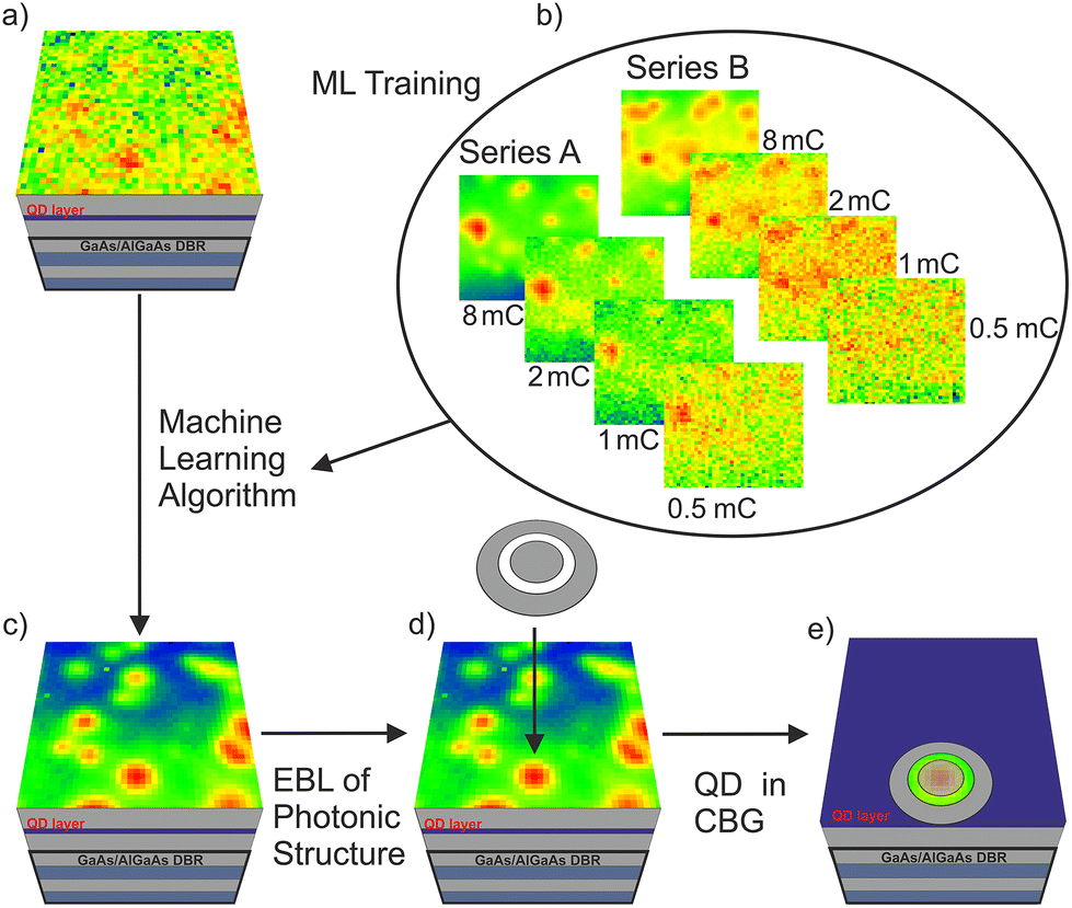 | ||
| Fig. 1 Basic principle of ML-enhanced in situ EBL. (a) Noisy CL-map in which a precise determination of QD positions is not possible. (b) Training of the ML algorithm by dose-dependent CL-maps of a QD sample. (c) ML-processed CL-map of (a) with significantly higher signal-to-noise ratio enabling the precise localization of QDs. (d) EBL writing of a one-ring CBG resonator aligned to a pre-selected QD. (e) Schematic view of the final QD-CBG device. | ||
A key goal of the employed ML algorithm is to reduce the noise level of CL-maps while improving the visibility of QDs. We decided to apply a ML algorithm based on an autoencoder used to denoise data sets from the Modified National Institute of Standards and Technology (MNIST) database50 which is optimized for finding specific features in noisy 2D images. More details about the ML algorithm are given in section 1. Before utilizing the ML algorithm for deterministic device integration, it has to be trained by suitable experimental data. In our case this means that training has to be performed using CL-maps with different SNRs as indicated in Fig. 1(b). For this purpose, we used the same sample material which was also used later for the ML-enhanced in situ EBL integration of QDs into CBG resonators.
Before growing the semiconductor heterostructures, the layer- and CBG-design was optimized for maximum photon extraction efficiency (PEE) using the finite element method (FEM) solver JCMsuite.51 The sample is based on an n-doped GaAs wafer. It includes a lower AlGaAs/GaAs distributed Bragg reflector and a GaAs capping layer into which a single layer of low-density InGaAs QDs is integrated. More details on the layer design and on the epitaxial growth are given in section 2. For ML training purposes we studied a planar piece of this heterostructure sample via low temperature CL mapping with integration times (electron beam doses) between 80 ms per pixel (8 mC cm−2) and 5 ms per pixel (0.5 mC cm−2). Here 8 mC cm−2 constitutes an optimized dose strength during in situ EBL to ensure that the resist is neither under- nor over-exposed in combination with the immediately following CBG patterning via EBL. Two examples (series A and B) of such series of CL-maps are presented in Fig. 1(b). Each map has a size of 20 × 20 μm2 and the electron beam dose was varied from 8 mC cm−2 to 0.5 mC cm−2. While QD positions are clearly identifiable at high dose values, the CL-maps are very noisy for the lowest dose of 0.5 mC cm−2, and especially for series B QD positions cannot be identified anymore. Noteworthy, we often observe CL-maps with SNRs values like that for telecom QDs which make deterministic device integration by conventional in situ EBL very difficult and strongly reduces the QD-nanostructure alignment accuracy.
Overall, 83 CL maps with the mentioned size of (20 × 20 μm2) at 12 different positions on the sample were taken as the data basis for ML training. Compared to typical ML training data sets consisting of thousands of images this is a rather small number, which can be increased in the future to obtain even better performances of ML-enhanced in situ EBL. In the present case, we took advantage of the fact that we do not only record the position dependent CL intensity but also the spectral information at each pixel of the CL map. This way, by feeding CL-maps with different spectral windows (with a width of 4–10 nm), and thus different QDs, in the overall spectral range of 880 nm to 954 nm we could efficiently expand the data base to a total of 279 CL-maps used for ML training.
Once trained, we applied the ML algorithm for the deterministic fabrication of bright single-photon sources (SPSs) based on single InGaAs QDs integrated into CBG resonators. This optimization process happened in the timespan of ≤1 min. The layer structure and CBG design parameters of these quantum light sources are shown in section 2. Essentially, the devices consist of a lower Al0.9Ga0.1As/GaAs DBR back reflector and a CBG formed by a central mesa and one ring. Compared to high-performance (hybrid) CBG SPSs with up to 9 rings and backside Au mirror yielding ηext > 70%,13,52 the structures chosen here are rather simple. Still, numeric optimization of the structures results in ηext ≈ 43% for a collective optics with a numerical aperture (NA) of 0.4 and a target emission wavelength of 945 nm. We chose this design because of the simpler fabrication process which allowed us to focus on the primary goal of the present work, namely, demonstrating the advantages of ML-enhanced in situ EBL, without elaborate device fabrication efforts.
The application of ML-enabled denoising of CL-maps is illustrated in Fig. 2. Here, we show three CL-maps with a size of 15 × 20 μm2 recorded at 8 mC cm−2 (panel (a)), 2 mC cm−2 (panel (b)), and 0.5 mC cm−2 (panel (c)), respectively, at the same sample position. We would like to note that later in the in situ EBL process the same map size (15 × 20 μm2) was used, to reduce the CL-mapping time to 1:57 minutes (for 8 mC cm−2), to mitigate the thermal shift of 14 nm min−1 of the sample stage in the used SEM system. As expected the SNR decreases form panel (a) to panel (c), and the pronounced QD emission spot at (x, y) = (4.7 μm, 15.5 μm) in panel (a) is very distorted and hardly visible in panel (c) at the lowest electron beam dose. Next, we determined the x–y coordinates for the same QD also for the CL-maps of panels (b) and (c) recorded at smaller dose through 2D-Gaussian fits. The fit accuracy is reduced from 14.4 nm to 130.1 nm with decreasing dose from panel (a) to (c), which in turn will also negatively affect the QD-CBG alignment accuracy. As the next step we applied the ML-algorithm trained to identify QD emission features in noise CL-maps to the data presented in panel (c). The result of this denoising procedure is presented in panel (d).
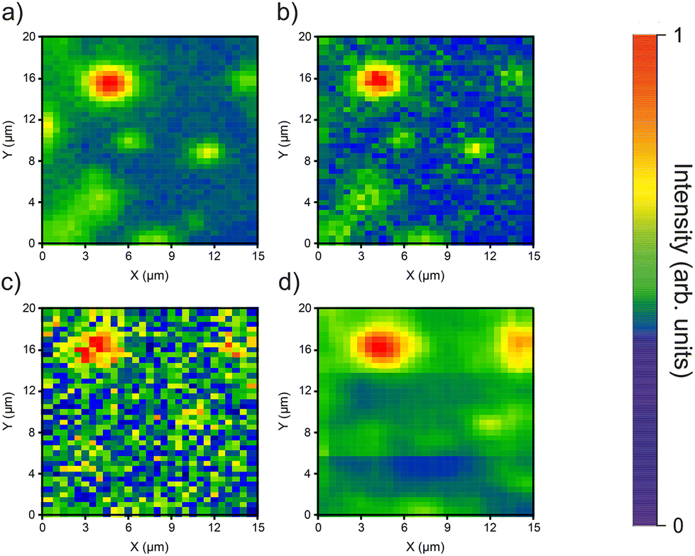 | ||
| Fig. 2 Comparison of CL-maps recorded at different dose levels and ML-enhanced CL-map. (a)–(c) show a CL intensity map of the same sample area which includes one prominent single QD in the upper left corner. The CL-maps were recorded for electron beam doses of 8 mC cm−2, 2 mC cm−2 and 0.5 mC cm−2 in (a), (b), and (c), respectively. (d) High-quality ML-enhanced CL-map obtained by denoising the data from (c). | ||
It is clearly visible that the quality of the image is strongly improved and comparable to the CL-map shown in panel (a) recorded with a factor 16 higher electron beam dose. This qualitative assessment is confirmed by comparing the widths of the respective 2D-Gaussian fits of 14.4 nm and 21.4 nm for the CL-maps recorded at 8 mC cm−2 (panel (a)) and the ML-denoised one recorded at 0.5 mC cm−2 (panel (d)). Within a systematic study of 102 QD positions in 102 different CL-mapping areas we investigated the ML-enhanced emitter localization accuracy for five different dose values in the range of 0.5 mC cm−2 to 8 mC cm−2. The results of this study are plotted in Fig. 3. For the unprocessed data the fit deviation (black data points) increases continuously from (32.4 ± 6.9) nm at a dose of 8 mC cm−2 to (129.7 ± 35.4) nm at the lowest dose of 0.5 mC cm−2, and it surpasses the in situ accuracy goal of 50 nm for CBG fabrication for dose values below 2 mC cm−2. In contrast, the fit deviation (red data points) of the ML-processed data stays below 50 nm in the whole studied dose range below 4 mC cm−2, and reaches a fit deviation of (40.2 ± 5.1) nm for the lowest dose of 0.5 mC cm−2. This is a central result of our work because it demonstrates that ML can indeed significantly improve the QD identification in noisy CL-maps to enable in situ EBL of dim quantum emitters, like telecom wavelength QDs, in the future. Interestingly, the fit accuracy even improves slightly with decreasing dose. This observation is explained by the fact the ML algorithm was specifically trained for pattern recognition in CL-maps with low SNR, which reflects the importance of training the ML algorithm for the correct target function. The obtained results clearly demonstrate the potential of ML-based image processing, which is in the following applied for deterministic in situ EBL device processing.
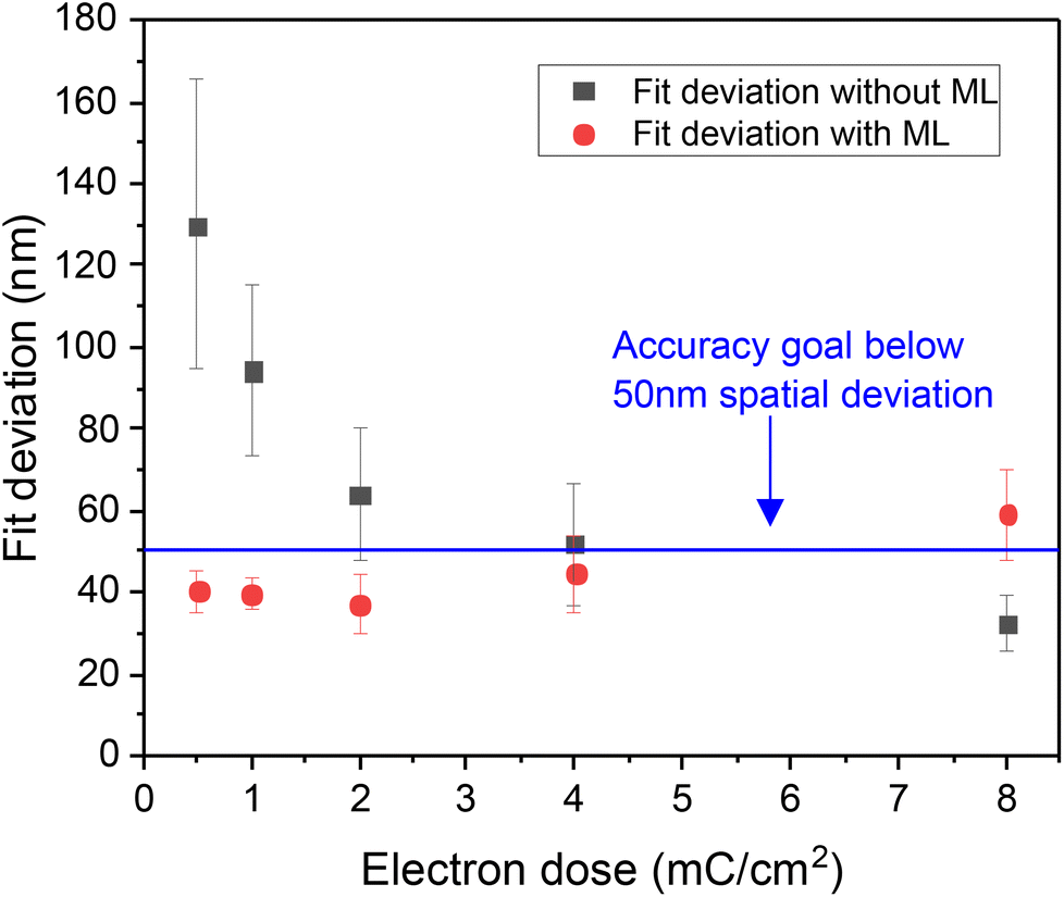 | ||
| Fig. 3 Statistical analysis of the deviation of the 2D-Gaussian fit to the emitter position in dependence of the electron beam dose with (red data points) and without (black data points) ML data processing. The accuracy goal (max. 50 nm deviation) for CBG fabrication via the in situ EBL process is indicated by the horizontal blue line. | ||
As the next step we performed deterministic in situ EBL processing of QD-CBG devices with and without ML CL-image processing. In this systematic study we again varied the mapping dose in the range of 0.5 mC cm−2 to 8 mC cm−2. In fact, CL-mapping needs to be performed in the positive tone regime of the EBL resist, with an onset dose of typically around 15 mC cm−2 for the negative tone regime. Thus, even for dim emitters the maximum dose is in practice typically limited to about 5–15 mC cm−2 and only ML-enhanced improvement of noisy CL-maps can enable a reliable in situ EBL device fabrication. Overall, we processed 93 QD-CBGs with and 98 QD-CBGs without ML processing of the CL maps.
The fabricated structures were studied by micro-photoluminescence (μPL) spectroscopy to assess the improvement of process yield when using ML-enhanced in situ EBL. Two exemplary (μPL) spectra of QD-CBG devices fabricated at a dose of 8 mC cm−2 without ML-enhanced processing (panel (a)) and with ML-enhanced processing and a dose of 0.5 mC cm−2 are presented in Fig. 4. Both spectra show distinct single-QD emission lines with very comparable emission intensity. This result shows that ML-enhanced processing at a significantly lower dose leads to a similar device quality than conventional in situ EBL fabrication. To underline this statement, the PEE was further investigated for the realized CBGs (section 3). Fig. 5(a) shows the PEE plotted over the mapping dose. Black data points correspond to structures fabricated by conventional in situ EBL and red data points are associated with structures fabricated by ML-enhanced in situ EBL. It can be clearly seen that the PEE for structures written without ML enhancement systematically decreases towards lower doses. On the other hand, applying ML enhancement leads to a significant improvement, reaching even at low doses PEE values ((34.8 ± 3.4)% at 1 mC cm−2) that are comparable to the ones at high doses ((35.6 ± 3.5)% at 8 mC cm−2) without ML. Those results are congruent with the data from Fig. 3 and even though there is quite some scattering in the plotted data, the (expected) overall trend of improved PEE in the case of ML-enhanced in situ EBL towards low dose values is clearly observed, as also supported by the black and red lines acting as guide to the eyes. We attribute part of the scattering to potential mismatches between the QD emission wavelength and the CBG mode and deviations in the desired structure dimensions (see section 2), both lowering the achievable PEE. Additionally, a large gap between the simulated (≈43%, blue line) and measured PEE is apparent. This is because the desired etch depth of 480 nm was not achieved due to a mismatch of the etching rate. An adjusted simulation for the measured etching depth of ≈520 nm yields a PEE of ≈35% (green line) which is in agreement with the experimental data. These promising results are further substantiated by an evaluation of all processed devices regarding optically active ones which show clear single-QD emission lines, as seen in Fig. 4, and others which are optically inactive. Here, optical inactivity is attributed to a non-successful QD integration because of insufficiently precise QD location in the CL-mapping step, mainly caused by a too noisy CL-map. The result of this evaluation is shown in Fig. 5(b), in which the fraction of optically active devices is plotted as a function of the electron beam dose applied in the CL-mapping process. Again, black data points correspond to structures fabricated by conventional in situ EBL and red data points are associated with structures fabricated by ML-enhanced in situ EBL. While a high ratio of optically active devices is obtained at high dose without ML denoising of the CL-maps, ML-enhanced in situ EBL clearly outperforms the conventional processing at low dose values with close to 80% (50%) optically active devices with (without) ML enhancement at a dose of 0.5 mC cm−2.
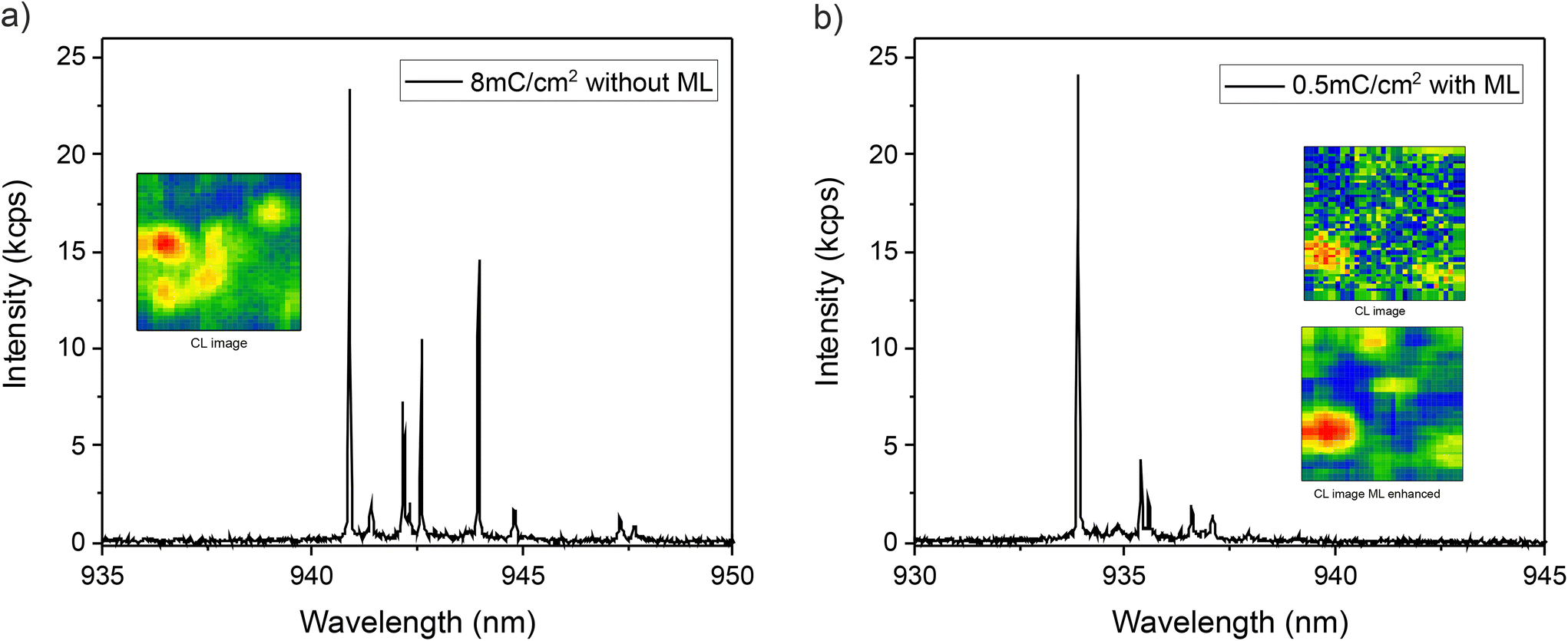 | ||
| Fig. 4 Optical characterization of deterministically fabricated QD-CBG devices. (a) μPL spectrum of a QD-CBG device fabricated by conventional in situ EBL using a CL mapping dose of 8 mC cm−2. (b) μPL spectrum of a QD-CBG device fabricated by ML enhanced in situ EBL. CL mapping was performed at a dose of 0.5 mC cm−2 followed by ML denoising. Insets show the corresponding CL maps with the QD (left corner) before and after ML enhancement. | ||
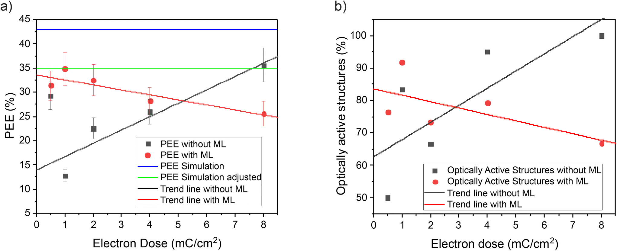 | ||
| Fig. 5 (a) Photon extraction efficiency PEE for QD-CBG devices with (red data points) and without (black data points) ML data processing in dependence of the electron beam dose applied in the QD-selection mapping step. The theoretical efficiency limit of ≈43% (blue line) is achieved for an etching depth of 430 nm. In experiment a depth of ≈520 nm was achieved, leading to a slightly lower simulated efficiency of ≈35% (green line) which is reached for the best structures. The red and black lines serve as guide to the eye and indicate a strongly improved process yield of ML-enhanced in situ EBL at low mapping doses if compared to conventional in situ EBL. (b) Fraction of optically active QD-CBG devices with (red data points) and without (black data points) ML data processing in dependence of the electron beam dose applied in the QD-selection mapping step. The red and black lines serve as guide to the eye and indicate a strongly improved process yield of ML-enhanced in situ EBL at low mapping doses if compared to conventional in situ EBL. | ||
3 Methods
3.1 Machine learning algorithm
The overarching goal of this work was to realize a ML algorithm which could sufficiently denoise 2D CL-maps of QDs to determine their positions through a 2D Gaussian fit. General approaches which are traditionally used to filter signals and enhance the signal-to-noise ratio are for example based on Fourier transformation or averaging over intensity values. Those constitute classical computer algorithms without the ability of pattern recognition. A classical algorithm is a sequence of single, consecutive commands and requests. Every step is a simple static instruction which is independent from the input value or an expected result. ML however, employs statistical models with a high number of free parameters and no physical laws or mathematical correlations are placed on this model, the parameters are simply optimized through a large number of training images. The code of the ML algorithm is based on an autoencoder used to denoise data sets from the MNIST database and had 28![[thin space (1/6-em)]](https://www.rsc.org/images/entities/char_2009.gif) 353 free parameters. The used applications were TensorFlow (version CPU 2.4.0) and the user interface Keras (version 2.4.0). Since Keras runs also on the computer processor, no graphics card was required to perform the necessary calculations. For training purposes 83 (20 × 20 μm2) CL-maps at 12 different positions with a E-beam dose range of 0.5 mC cm−2 to 8 mC cm−2 were obtained. This is a highly insufficient amount to train the ML algorithm considering that test trials with data from MNIST delivered acceptable results for 7500–10000 training images. Since the CL-maps also contained spectral information at each pixel with a range of 880 nm to 954 nm, it was possible to extent the available data to 279 maps by examine different spectral windows. Being still orders of magnitude from the required amount away, each CL-map was divided into submaps. The submaps were created by moving a window of 28 × 28 pixel with a step size of 5 pixel over the CL-map. As a consequence, the pooling-function of the autoencoder, which is responsible for the downsampling, always received a different pixel group. This method resulted in a total of 26880 available maps which made the training of the ML algorithm possible.
353 free parameters. The used applications were TensorFlow (version CPU 2.4.0) and the user interface Keras (version 2.4.0). Since Keras runs also on the computer processor, no graphics card was required to perform the necessary calculations. For training purposes 83 (20 × 20 μm2) CL-maps at 12 different positions with a E-beam dose range of 0.5 mC cm−2 to 8 mC cm−2 were obtained. This is a highly insufficient amount to train the ML algorithm considering that test trials with data from MNIST delivered acceptable results for 7500–10000 training images. Since the CL-maps also contained spectral information at each pixel with a range of 880 nm to 954 nm, it was possible to extent the available data to 279 maps by examine different spectral windows. Being still orders of magnitude from the required amount away, each CL-map was divided into submaps. The submaps were created by moving a window of 28 × 28 pixel with a step size of 5 pixel over the CL-map. As a consequence, the pooling-function of the autoencoder, which is responsible for the downsampling, always received a different pixel group. This method resulted in a total of 26880 available maps which made the training of the ML algorithm possible.
3.2 Device design
The device design for our study was optimized using the FEM solver JCMsuite. The goal was to achieve maximum outcoupling efficiency whilst keeping the layout simple in order to put the main focus or our present work on the development and evaluation of ML-enhanced in situ EBL. Based on the optimized layer design, first the back-side Al0.9Ga0.1As/GaAs DBR with 23 mirror pairs (see Fig. 6(a)) having layer thicknesses of 79 nm and 67 nm, respectively, was grown on a 2-inch n-doped GaAs wafer. Subsequently, 158 nm of GaAs were grown, followed by the QD-layer (In0.38Ga0.62As) which was then capped by additional 275 nm of GaAs. For this layout, CBG designs were optimized resulting in a central mesa with a radius of 339 nm, a surrounding 416 nm wide trench and a 504 nm-thick ring. The optimal etching depth for those parameters was 480 nm, etching deep inside the last GaAs-layer of the DBR. This device design results in a simulated PEE of ≈43% for a collection optics with an NA = 0.4 and a target emission wavelength of 945 nm. The corresponding electric field distribution is presented in Fig. 6(b). Furthermore, the design leads to broadband enhancement over a wide wavelength range of approximately 30 nm (FMHM). Noteworthy, adding further rings to the CBG does not have a positive effect on ηext in the chosen design. However, additional rings lead to higher directionality of emission, which can be beneficial for on-ship fiber coupling. An SEM image of a fully processed structure depicted in Fig. 6(c).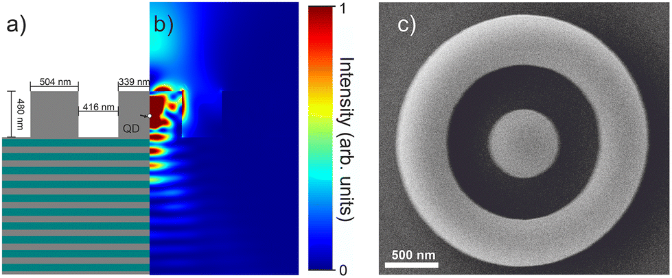 | ||
| Fig. 6 (a) Schematic illustration of the device design (cross-section of half the structure). The layer structure consists of an Al0.9Ga0.1As (green)/GaAs (grey) DBR with 23 λ/4-thick mirror pairs and a single low density layer of self-assembled In0.38Ga0.62As QDs, which are embedded 275 nm below the surface of the 433 nm thick GaAs capping layer. The layer structure and the geometry of the one-ring QD-CBG resonator was optimized by FEM simulations which yield ηext = ≈43% for an NA of 0.4. (b) Simulated electric field strength distribution in the device. (c) SEM image of a fabricated QD-CBG device. | ||
3.3 Experimental setups
4 Conclusions
In summary, we developed an advanced deterministic nanofabrication technology for the fabrication of single-emitter quantum photonic devices. To be more precise, we applied ML-based denoising of CL intensity maps to improve the QD pre-selection capabilities of in situ EBL. The developments include the target-specific training of a ML algorithm optimized for image processing using CL-maps recorded on a QD sample at different electron beam dose values. This training aimed at reliable identification of QDs in noisy CL intensity maps and a statistical evaluation of the achieved results show a remarkable improvement of the QD pre-selection accuracy and photon extraction efficiency of ML-enhanced in situ EBL in comparison to conventional in situ EBL. Indeed, in case of ML-enhanced processing the QD positions can still be precisely determined at dose values more than a factor of ten lower than used in conventional in situ EBL, while still achieving the same PEE. These results are very promising with regard to the deterministic device integration of single quantum emitters with low luminescence yield, such as telecom-wavelength QDs. Indeed, first tests on CL-maps with QDs in the telecom C-band show promising results, even though our ML algorithm was trained with CL data obtained for QDs emitting at lower wavelengths. This leads us to believe that ML-based image processing of noisy CL maps can strongly improve the QD-selection and device-alignment accuracy to increase the process yield and to optimize the optical properties of these quantum devices. Furthermore, our reported approach is not only limited to the here used in situ electron beam lithography but could be extended to all technologies which require accurate position determination based on 2D luminescence maps.Author contributions
J. D. and M. S. performed the CL experiments and CL lithography with support from M. P. and J. S., J. D., M. S. and L. B. carried out the μPL investigations. M. S. programmed the machine learning algorithm. S. R. and J. D. conducted the numerical modelling. C. S. grew the samples with support from I. L. The sample was processed in the clean room by J. D. Sven Rodt and Stephan Reitzenstein initiated the research, supervised the project and wrote the manuscript with input from all authors.Conflicts of interest
There are no conflicts to declare.Acknowledgements
This work was supported by the German Research Foundation (DFG) via projects Re2974/20-1, Re2974/23-1 and Re2974/25-1, by the German Federal Ministry of Education and Research (BMBF) via the project QR.X, and by the Volkswagen Foundation via the project NeuroQNet II. We thank Lucas Rickert for valuable discussions and technical support.References
- N. Gisin and R. Thew, Nat. Photonics, 2007, 1, 165–171 CrossRef CAS.
- T. Northup and R. Blatt, Nat. Photonics, 2014, 8, 356–363 CrossRef CAS.
- F. Flamini, N. Spagnolo and F. Sciarrino, Rep. Prog. Phys., 2018, 82, 016001 CrossRef PubMed.
- I. Aharonovich and E. Neu, Adv. Opt. Mater., 2014, 2, 911–928 CrossRef CAS.
- I. Aharonovich, D. Englund and M. Toth, Nat. Photonics, 2016, 10, 631–641 CrossRef CAS.
- Y.-M. He, G. Clark, J. Schaibley, Y. He, M.-C. Chen, Y.-J. Wei, X. Ding, Q. Zhang, W. Yao, X. Xu, C.-Y. Lu and J.-W. Pan, Nat. Nanotechnol., 2015, 10, 497–502 CrossRef CAS.
- S. Ren, Q. Tan and J. Zhang, J. Semicond., 2019, 40, 071903 CrossRef CAS.
- Y. Arakawa and M. Holmes, Appl. Phys. Rev., 2020, 7, 021309 CAS.
- S. Hepp, M. Jetter, S. Portalupi and P. Michler, Adv. Quantum Technol., 2019, 2, 1900020 CrossRef.
- M. Gschrey, A. Thoma, P. Schnauber, M. Seifried, R. Schmidt, B. Wohlfeil, L. Krüger, J.-H. Schulze, T. Heindel, S. Burger, F. Schmidt, A. Strittmatter, S. Rodt and S. Reitzenstein, Nat. Commun., 2015, 6, 7662 CrossRef CAS PubMed.
- A. Thoma, P. Schnauber, M. Gschrey, M. Seifried, J. Wolters, J.-H. Schulze, A. Strittmatter, S. Rodt, A. Carmele, A. Knorr, T. Heindel and S. Reitzenstein, Phys. Rev. Lett., 2016, 116, 033601 CrossRef CAS PubMed.
- X. Ding, Y. He, Z.-C. Duan, N. Gregersen, M.-C. Chen, S. Unsleber, S. Maier, C. Schneider, M. Kamp, S. Höfling, C.-Y. Lu and J.-W. Pan, Phys. Rev. Lett., 2016, 116, 028301 CrossRef PubMed.
- J. Liu, R. Su, Y. Wei, B. Yao, S. Silva, Y. Yu, J. Iles-Smith, K. Srinivasan, A. Rastelli, J. Li and X. Wang, Nat. Nanotechnol., 2019, 14, 586–593 CrossRef CAS PubMed.
- H. Wang, Y.-M. He, T.-H. Chung, H. Hu, Y. Yu, S. Chen, X. Ding, M.-C. Chen, J. Qin, X. Yang, R.-Z. Liu, Z.-C. Duan, J.-P. Li, S. Gerhardt, K. Winkler, J. Jurkat, L.-J. Wang, N. Gregersen, Y.-H. Huo, Q. Dai, S. Yu, S. Höfling, C.-Y. Lu and J.-W. Pan, Nat. Photonics, 2019, 13, 770–775 CrossRef CAS.
- N. Somaschi, V. Giesz, L. De Santis, J. Loredo, M. Almeida, G. Hornecker, S. Portalupi, T. Grange, C. Antón, J. Demory, C. Gómez, I. Sagnes, N. Lanzillotti-Kimura, A. Lemaítre, A. Auffeves, A. White, L. Lanco and P. Senellart, Nat. Photonics, 2016, 10, 340–345 CrossRef CAS.
- Y.-J. Wei, Y.-M. He, M.-C. Chen, Y.-N. Hu, Y. He, D. Wu, C. Schneider, M. Kamp, S. Höfling, C.-Y. Lu and J.-W. Pan, Nano Lett., 2014, 14, 6515–6519 CrossRef CAS PubMed.
- L. Schweickert, K. Jöns, K. Zeuner, S. Covre Da Silva, H. Huang, T. Lettner, M. Reindl, J. Zichi, R. Trotta, A. Rastelli and V. Zwiller, Appl. Phys. Lett., 2018, 112, 093106 CrossRef.
- P. Schnauber, A. Singh, J. Schall, S. Park, J. Song, S. Rodt, K. Srinivasan, S. Reitzenstein and M. Davanco, Nano Lett., 2019, 19, 7164–7172 CrossRef CAS PubMed.
- S. Rodt and S. Reitzenstein, APL Photonics, 2021, 6, 010901 CrossRef.
- A. Hartmann, L. Loubies, F. Reinhardt and E. Kapon, Appl. Phys. Lett., 1997, 71, 1314–1316 CrossRef CAS.
- H. Song, T. Usuki, S. Hirose, K. Takemoto, Y. Nakata, N. Yokoyama and Y. Sakuma, Appl. Phys. Lett., 2005, 86, 113118 CrossRef.
- M. Reimer, W. Mckinnon, J. Lapointe, D. Dalacu, P. Poole, G. Aers, D. Kim, M. Korkusiński, P. Hawrylak and R. Williams, Phys. E, 2008, 40, 1790–1793 CrossRef.
- F. Albert, S. Stobbe, C. Schneider, T. Heindel, S. Reitzenstein, S. Höfling, P. Lodahl, L. Worschech and A. Forchel, Appl. Phys. Lett., 2010, 96, 151102 CrossRef.
- A. Strittmatter, A. Holzbecher, A. Schliwa, J.-H. Schulze, D. Quandt, T. Germann, A. Dreismann, O. Hitzemann, E. Stock, I. Ostapenko, S. Rodt, W. Unrau, U. Pohl, A. Hoffmann, D. Bimberg and V. Haisler, Phys. Status Solidi A, 2012, 209, 2411–2420 CrossRef CAS.
- J. Canet-Ferrer, G. Munoz-Matutano, J. Herranz, D. Rivas, B. Alen, Y. Gonzalez, D. Fuster, L. Gonzalez and J. Martínez-Pastor, Appl. Phys. Lett., 2013, 103, 183112 CrossRef.
- M. Holmes, K. Choi, S. Kako, M. Arita and Y. Arakawa, Nano Lett., 2014, 14, 982–986 CrossRef CAS.
- D. Cadeddu, J. Teissier, F. Braakman, N. Gregersen, P. Stepanov, J.-M. Gérard, J. Claudon, R. Warburton, M. Poggio and M. Munsch, Appl. Phys. Lett., 2016, 108, 011112 CrossRef.
- J.-H. Kim, S. Aghaeimeibodi, C. Richardson, R. Leavitt, D. Englund and E. Waks, Nano Lett., 2017, 17, 7394–7400 CrossRef CAS.
- A. Elshaari, I. Zadeh, A. Fognini, M. Reimer, D. Dalacu, P. Poole, V. Zwiller and K. Jöns, Nat. Commun., 2017, 8, 379 CrossRef PubMed.
- T. Kojima, K. Kojima, T. Asano and S. Noda, Appl. Phys. Lett., 2013, 102, 011110 CrossRef.
- G. Nogues, Q. Merotto, G. Bachelier, E. Hye Lee and J. Dong Song, Appl. Phys. Lett., 2013, 102, 231112 CrossRef.
- M. Pfeiffer, K. Lindfors, H. Zhang, B. Fenk, F. Phillipp, P. Atkinson, A. Rastelli, O. Schmidt, H. Giessen and M. Lippitz, Nano Lett., 2013, 14, 197–201 CrossRef PubMed.
- L. Sapienza, M. Davanço, A. Badolato and K. Srinivasan, Nat. Commun., 2015, 6, 7833 CrossRef CAS PubMed.
- M. Sartison, S. Portalupi, T. Gissibl, M. Jetter, H. Giessen and P. Michler, Sci. Rep., 2017, 7, 39916 CrossRef CAS PubMed.
- A. Dousse, L. Lanco, J. Suffczyński, E. Semenova, A. Miard, A. Lemaître, I. Sagnes, C. Roblin, J. Bloch and P. Senellart, Phys. Rev. Lett., 2008, 101, 267404 CrossRef CAS PubMed.
- F. Donatini and L. Dang, Nanotechnology, 2010, 21, 375303 CrossRef PubMed.
- S. Unsleber, Y.-M. He, S. Gerhardt, S. Maier, C.-Y. Lu, J.-W. Pan, N. Gregersen, M. Kamp, C. Schneider and S. Höfling, Opt. Express, 2016, 24, 8539 CrossRef CAS PubMed.
- M. Gschrey, F. Gericke, A. Schüßler, R. Schmidt, J.-H. Schulze, T. Heindel, S. Rodt, A. Strittmatter and S. Reitzenstein, Appl. Phys. Lett., 2013, 102, 251113 CrossRef.
- S. Rodt and S. Reitzenstein, Nano Express, 2021, 2, 014007 CrossRef.
- P.-I. Schneider, N. Srocka, S. Rodt, L. Zschiedrich, S. Reitzenstein and S. Burger, Opt. Express, 2018, 26, 8479 CrossRef CAS PubMed.
- W. Ma, F. Cheng and Y. Liu, ACS Nano, 2018, 12, 6326–6334 CrossRef CAS.
- J. Wei, X. Chu, X. Sun, K. Xu, H. Deng, J. Chen, Z. Wei and M. Lei, InfoMat, 2019, 1, 338–358 CrossRef CAS.
- Z. Kudyshev, S. Bogdanov, T. Isacsson, A. Kildishev, A. Boltasseva and V. Shalaev, Adv. Quantum Technol., 2020, 3, 2000067 CrossRef CAS.
- A. L. Samuel, IBM J. Res. Dev., 1959, 3, 210–229 Search PubMed.
- J. Shen, Y. Liu, S. Wang and Z. Sun, 2014 European Modelling Symposium, 2014.
- A. Habibian, T. V. Rozendaal, J. Tomczak and T. Cohen, 2019 IEEE/CVF International Conference on Computer Vision (ICCV), 2019.
- W.-H. Peng and H.-M. Hang, 2020 IEEE International Conference on Visual Communications and Image Processing (VCIP), 2020.
- L. Tuggener, M. Amirian, K. Rombach, S. Lorwald, A. Varlet, C. Westermann and T. Stadelmann, 2019 6th Swiss Conference on Data Science (SDS), 2019.
- Y. Xu, X. Liu, X. Cao, C. Huang, E. Liu, S. Qian, X. Liu, Y. Wu, F. Dong, C.-W. Qiu, J. Qiu, K. Hua, W. Su, J. Wu, H. Xu, Y. Han, C. Fu, Z. Yin, M. Liu, R. Roepman, S. Dietmann, M. Virta, F. Kengara, Z. Zhang, L. Zhang, T. Zhao, J. Dai, J. Yang, L. Lan, M. Luo, Z. Liu, T. An, B. Zhang, X. He, S. Cong, X. Liu, W. Zhang, J. P. Lewis, J. M. Tiedje, Q. Wang, Z. An, F. Wang, L. Zhang, T. Huang, C. Lu, Z. Cai, F. Wang and J. Zhang, Innovation, 2021, 2, 100179 Search PubMed.
- Y. LeCun, C. Cortes and C. J. C. Burges, The MNIST Database of Handwritten Digits, New York, USA, 1998.
- https://jcmwave.com/jcmsuite .
- H. Wang, H. Hu, T.-H. Chung, J. Qin, X. Yang, J.-P. Li, R.-Z. Liu, H.-S. Zhong, Y.-M. He, X. Ding, Y.-H. Deng, Q. Dai, Y.-H. Huo, S. Höfling, C.-Y. Lu and J.-W. Pan, Phys. Rev. Lett., 2019, 122, 113602 CrossRef CAS PubMed.
| This journal is © The Royal Society of Chemistry 2022 |