
 Open Access Article
 This Open Access Article is licensed under a
 Creative Commons Attribution 3.0 Unported Licence
A unique physics-inspired deep-learning-based platform introducing a generalized tool for rapid optical-response prediction and parametric-optimization for all-dielectric metasurfaces
Sadia
Noureen
a,
Muhammad Qasim
Mehmood
 *a,
Mohsen
Ali
b,
Bacha
Rehman
c,
Muhammad
Zubair
*a and
Yehia
Massoud
*d
*a,
Mohsen
Ali
b,
Bacha
Rehman
c,
Muhammad
Zubair
*a and
Yehia
Massoud
*d
aMicroNano Lab, Electrical Engineering Department, Information Technology University (ITU) of the Punjab, Ferozepur Road, Lahore 54600, Pakistan. E-mail: muhammad.zubair@itu.edu.pk; qasim.mehmood@itu.edu.pk
bDepartment of Computer Science, Information Technology University (ITU) of the Punjab, Arfa Software Technology Park, Ferozepur Road, Lahore 54600, Pakistan
cNAMAL University, Mianwali, Pakistan
dInnovative Technologies Laboratories (ITL), King Abdullah University of Science and Technology (KAUST), Saudi Arabia. E-mail: yehia.massoud@kaust.edu.sa
First published on 3rd November 2022
Abstract
Metasurfaces are composed of a two-dimensional array of carefully engineered subwavelength structures. They provide a novel compact alternative to conventional voluminous optical components. However, their design involves a time-consuming hit and trial procedure, requiring many iterative electromagnetic simulations through expensive commercial solvers. To overcome this non-practical design strategy, recently, various deep-learning-based fast and low computational cost networks have been proposed to design and optimize individual meta-atoms and complete metasurfaces. Most of them focus on optimizing the amplitude response of nanostructures, whereas mapping the phase response is a much more challenging problem that needs to be addressed. Since the metaatom's optical response is entirely reliant on and vulnerable to its geometrical structure, underlying material, and operating wavelength, changing any of these parameters changes the entire physics of the problem in hand. Here, we propose novel deep-learning-based generalized forward and inverse design approaches to optimize all-dielectric transmissive metasurfaces. The proposed forward predicting neural networks take all the geometrical parameters and the physical properties of the bar-shaped dielectric nano-resonators as the input and predict the cross-polarized transmission amplitude and modulated phase at eight distinct rotation angles of the nano-bar. These networks are generalized to predict the electromagnetic (EM) response of different dielectric materials at different operating wavelengths. An inverse design neural network is also proposed that takes the target transmission amplitude and phase at eight discrete orientation angles of the nano-bar as the primary input. The underlying physics of the problem is also incorporated by feeding the intrinsic material properties and the operating wavelength of the nano-bar as a second input to the inverse neural network. It predicts the optimum set of geometrical parameters to achieve maximum cross-polarized transmission and complete Pancharatnam–Berry (PB) phase coverage from 0 to 2π. The average test data mean square error (MSE) achieved for the forward predicting neural network is 1.8 × 10⁻³ and that of the inverse design neural network is 2.8 × 10⁻¹. The average MSEs for different material's test samples are demonstrated to validate the generalizability of the proposed models in terms of seen and unseen materials. A comparative analysis of the proposed approach with conventional EM software optimization tools is performed to prove that the proposed inverse design works much faster than the conventional methods, also it can handle a comparatively larger range of parameters and predicts the results in a single run with high accuracy.
1 Introduction
Metasurfaces, emerged as the planar counterparts of bulky optical components,1,2 can tailor the phase, polarization, and amplitude of incident electromagnetic waves3,4 in a desired manner. Metasurfaces can be engineered to realize different meta-optical phenomena such as ultra-thin flat lenses,5 filters,6,7 orbital angular momentum generation,8 optical vortex generation,9,10 holograms,11–13 absorbers,14–17 metamirrors,18 optical imaging,19 non-diffracting beams,20,21etc.Recently, metasurfaces having all-dielectric unit elements have come forth as the more efficient and less lossy (due to negligible ohmic losses in the optical domain) counterparts for metallic metasurfaces.22–24 This high efficiency is due to the formation of complex electric and magnetic multipole resonances. Electromagnetic dipoles, quadrupoles, and other higher-order poles formed in dielectric resonators have a significant yet unpredictable effect on the output EM response and they cause abrupt discontinuities in the phase response, i.e., 0°–180° and 180°–0°. Also, these resonances are directly dependent on a metasurface's unit cell geometry.25 Therefore, it is very difficult to map the effect of a unit cell's structural parameters and the resulting resonances on the phase and amplitude of the incident EM wave. In this regard, traditional analytical modeling tools for nano-structures26–29 and metasurfaces such as the GEM (generalized effective-medium theory) model30 and the Lewin model31 also fail to provide accurate results when the operating wavelength becomes comparable to a unit cell's size. Therefore, we need a fast and efficient solution to accurately predict the EM response of an all-dielectric unit element and to perform the inverse, i.e., find an all-dielectric unit element's optimized geometrical parameters and orientation to match with specific design targets for specific applications. The conventional approach to address this problem is to perform iterative full-wave electromagnetic simulations using expensive commercial software, resulting in a highly time-tedious and computationally exhaustive procedure, although it results in a model with accurate response predictions. Keeping in view the vast potential of deep neural networks (DNNs) to solve complex scientific problems,32,33 various models of DNNs have been suggested to expedite dielectric metasurface modeling34–36 and explore the dormant connection between a nano resonator and its EM response.37,38 The related work in this field is discussed in the next paragraph.
Deep learning based metasurface modeling approaches have turned out to be very effective to predict the EM amplitude response39–41 and performing inverse design for it. However, the prediction of phase and the optimization of dielectric resonators for full phase coverage is a much more challenging problem due to the abrupt discontinuities as discussed in the previous paragraph. Phase prediction failures allow us to design only those metasurfaces which don't require bending light at various angles by each nanoresonator such as absorbers, colour filters, etc. It severely restricts the accuracy of designing phase-based meta-devices such as meta-lenses, meta-holographs or deflectors using DNNs or related approaches. Recently, conditional and Wasserstein generative adversarial networks (GANs) were proposed to predict the amplitude and phase response of dielectric nanostructures and perform inverse design optimization as well.42,43 However, in addition to the complex and data-hungry nature of GANs, they only predict 2D images of 3D nanostructures, thus the materials properties, wavelength effects, and the geometrical attributes of dielectric structures are ignored. Later on, tandem neural network based approaches were also proposed, but they require separate networks to predict phase and amplitude responses, also they don't consider the material properties and they can handle only a limited number of input geometrical parameters.44 Some researchers developed neural network based closed loop models to optimize a single variable at a time by fixing other, which puts a limit on the number of parameters to be optimized and affects the dependency of one parameter on the other.45 The use of a simple predicting neural network (PNN) for forward design and tandem networks for inverse design was also proposed using the real and imaginary parts of the EM response as labels.46 Although the results were quite promising, again it required training two separate networks to predict the real and imaginary parts, respectively. To perform inverse design, the two separate networks need to use the same inputs while having their respective losses and gradients. This may cause conflict and optimization may not converge, obstructing the inverse design procedure. Therefore, we need a simple yet time-efficient model to predict the collective amplitude and phase response of all dielectric 3D nanostructures, and to perform their inverse optimization, while taking all the geometrical parameters, material properties and operating wavelengths into account.
In this paper, we present a unique methodology to design all-dielectric metasurfaces using deep neural networks, which addresses all the challenges discussed above. The proposed forward networks are capable of predicting the amplitude and phase response of each candidate bar-shaped unit cell at eight distinct orientation angles. It is demonstrated that inverse design DNNs are also capable of predicting optimized geometrical parameters of dielectric bar-shaped unit cells to achieve maximum transmission, and full phase coverage when the bar is rotated from 0° to 180°. Intrinsic properties of the dielectrics and the operating wavelengths (covering the whole visible regime) are also incorporated in the proposed DNNs to map their effect on the optimized parameters. Adding these properties in the inverse design network saves us from the redundant efforts of repeating the conventional iterative optimization procedure again and again from scratch for any change in the material or wavelength. Thus it allows fast and efficient determination of non-intuitive multi-functional device designs. A comparative analysis of the proposed approach with conventional EM software optimization tools is also performed to validate the accuracy and time efficiency of our model. Table 1 shows the comparison of the salient features of the proposed methodology with the previously reported methodologies for forward and inverse design approaches of metasurfaces.
| Forward prediction approach | |||||
| Methodology | Input features considered | Output predictions | |||
| Geometrical parameters | Diverse materials’ intrinsic properties | Different operating wavelengths | Amp | Phase | |
| Deep neural network37 (FC layers + transposed conv. + conv. layers) | ✓ | ✗ | ✗ | ✓ | ✗ |
| DNN CNNs + FC-NNs39 | ✗ Only shape | ✗ | ✗ | ✓ | ✗ |
| DNN40 | Only half of the parameters considered | ✗ | ✗ | ✓ | ✓ |
| DNN41 | ✓ | ✓ | ✓ | ✓ | ✓ |
| Proposed forward model: multi input multi output DNN | ✓ | ✓ | ✓ | ✓ | ✓ |
| Inverse design approach | |||||
| Methodology | Input | Output | |||
| Target amp | Target phase | Diverse target material properties | Diverse target wavelength | Simultaneous prediction of the geometrical parameter | |
| Fast forward dictionary search37 | ✓ | ✗ | ✗ | ✗ | ✓ |
| cGAN39 | ✓ | ✗ | ✗ | ✗ | ✗ |
| Tandem neural network40 | ✗ | ✓ | ✗ | ✗ | Limited number of parameters predicted |
| Modified version of tandem learning approach41 | ✗ | ✓ | ✓ | ✓ | ✗ Predicts one parameter at a time by fixing others. |
| Proposed inverse design multi input multi output DNN | ✓ | ✓ | ✓ | ✓ | ✓ |
2 Methodology
This work focuses on the design development of amplitude and phase engineered all-dielectric metasurfaces operating in the visible regime. Fig. 1 shows the prototype unit cell of the metasurface under consideration. Each unit cell consists of a dielectric nano-bar laid over a glass substrate. We have particularly chosen a rectangular bar shaped structure as it is easier to prepare, exhibits birefringence nature, and provides polarization sensitivity and broadband capacity. Each unit cell is parameterized by the bar's 3D geometrical parameters i.e., height (H), width (w), length (L), periodicity (P), and the material's physical properties i.e., the refractive index (n) and extinction coefficient (k). An alteration in any of these parameters will have a direct effect on the multipole resonances excited in the unit cell, which in turn affects the output amplitude and phase. Therefore, we present forward predicting neural networks, which take into account all these parameters, to map the dependency of the output on each of these factors. Thus, our forward predicting NN behaves very similarly to conventional EM software, takes all the inputs in a similar fashion, but predicts the output amplitude and phase within seconds and without the need of any iteration simulations to solve the Maxwell equations on a case-by-case basis.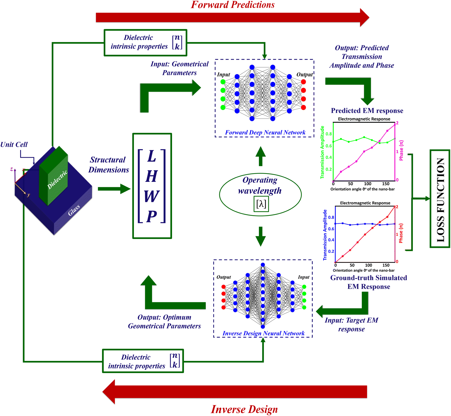 | ||
| Fig. 1 A pictorial representation of the proposed forward and inverse design models. The forward predicting network takes the structural dimensions, dielectric intrinsic properties and operating wavelength as the input and predicts the cross-polarized transmission amplitude and phase. The inverse model takes the target EM response as the input, along with the material and desired wavelength specifications as the input, to predict optimum geometrical parameters as the output. | ||
The proposed DNN-based forward design model is capable of predicting the optical response of dielectric nano-bars having different dimensions, composed of different materials (having different n and k), and operating at different visible wavelengths, whereas the inverse design model takes the target optical response, the physical properties of the material, and the wavelength as an input, and predicts the optimum geometrical parameters of the nano-bar to achieve the desired response. Unlike conventional EM software where we have to rerun the simulations for any change in the bar's material or operating wavelength, the proposed forward and inverse designs are generalized to predict the optical response and the optimum structural parameters for multiple dielectric materials and broadband visible wavelengths without retraining the networks again and again. A pictorial illustration of the proposed models is shown in Fig. 1.
For the composition of the nano-bars, we have selected six of the most suitable high refractive index dielectric materials which exhibit transparency over some part or the entire wavelength range of the visible domain. The materials selected are hydrogenated amorphous silicon (a-Si![[thin space (1/6-em)]](https://www.rsc.org/images/entities/char_2009.gif) :H), titanium dioxide (TiO2), hydrogenated phosphorus-doped modified amorphous silicon, silicon nitride (Si3N4), gallium phosphide (GaP) and gallium nitride (GaN). Rectangular bars with optimized dimensions made up of any of these materials can be periodically placed over a glass substrate to achieve the desired meta-optical phenomenon. Among these materials, silicon nitride is used as an unseen material for the DNN, all the other materials are a part of both the training and the test datasets but Si3N4 is part of the test dataset only. Since the material properties are a function of the operating wavelength, the target wavelength is also fed as an input to the proposed models. For instance, we have considered six different optical wavelengths to represent six different colors i.e., 633 nm – red, 600 nm – orange, 580 nm – yellow, 550 nm – green, 480 nm – blue, and 404 nm – violet. The intrinsic properties, n, and k of selected materials with respect to the wavelengths are presented in Table 2.
:H), titanium dioxide (TiO2), hydrogenated phosphorus-doped modified amorphous silicon, silicon nitride (Si3N4), gallium phosphide (GaP) and gallium nitride (GaN). Rectangular bars with optimized dimensions made up of any of these materials can be periodically placed over a glass substrate to achieve the desired meta-optical phenomenon. Among these materials, silicon nitride is used as an unseen material for the DNN, all the other materials are a part of both the training and the test datasets but Si3N4 is part of the test dataset only. Since the material properties are a function of the operating wavelength, the target wavelength is also fed as an input to the proposed models. For instance, we have considered six different optical wavelengths to represent six different colors i.e., 633 nm – red, 600 nm – orange, 580 nm – yellow, 550 nm – green, 480 nm – blue, and 404 nm – violet. The intrinsic properties, n, and k of selected materials with respect to the wavelengths are presented in Table 2.
| Wavelength | a-Si:H |
TiO2 | GaN | GaP | Mod. a-Si:H |
Si3N4 | ||||||
|---|---|---|---|---|---|---|---|---|---|---|---|---|
| N | K | N | k | n | K | n | k | N | k | n | k | |
| 633 nm | 3.25 | 0.047 | 1.88 | 0.001 | 2.38 | 0 | 3.31 | 0 | 2.88 | 0.001 | 2.039 | 0 |
| 600 nm | 3.29 | 0.06 | 1.89 | 0.0017 | 2.39 | 0 | 3.36 | 0 | 2.92 | 0.003 | 2.044 | 0 |
| 580 nm | 3.33 | 0.076 | 1.9 | 0.0018 | 2.40 | 0 | 3.4 | 0 | 2.96 | 0.005 | 2.047 | 0 |
| 550 nm | 3.39 | 0.101 | 1.91 | 0.002 | 2.41 | 0 | 3.45 | 0 | 3.02 | 0.008 | 2.05 | 0 |
| 480 nm | 3.59 | 0.19 | 1.94 | 0.003 | 2.45 | 0 | 3.67 | 0.01 | 3.23 | 0.065 | 2.068 | 0 |
| 404 nm | 4.06 | 0.49 | 2.01 | 0.005 | 2.55 | 0 | 4.16 | 0.26 | 3.59 | 0.311 | 2.098 | 0 |
A forward design regression based deep neural network is proposed to replace the time-consuming and computationally exhaustive EM simulations for evaluating the performance of metasurfaces. The proposed network is a unique data-driven model capable of accurately predicting both the amplitude and phase response of 3D all-dielectric nanostructures. The structural dimensions (height, width, length and periodicity), the intrinsic properties (n and k), and the operating wavelength of the nano-bars define their output electromagnetic response. Keeping the incident light the same and varying any of these parameters will vary the output response, therefore all these parameters are considered as the input variables of the proposed forward design multi-input multi-output regression neural network. Each input sample is a 1D column vector with 7 rows representing L, W, H, P, n, k, and λ as shown in Fig. 1. Output labels will be the phase and amplitude response of the sample unit cell. Thus, the forward problem can be mathematically expressed as:
| [ϕ, A] = fL,W,H,P,n,k,λ(Eincident) | (1) |
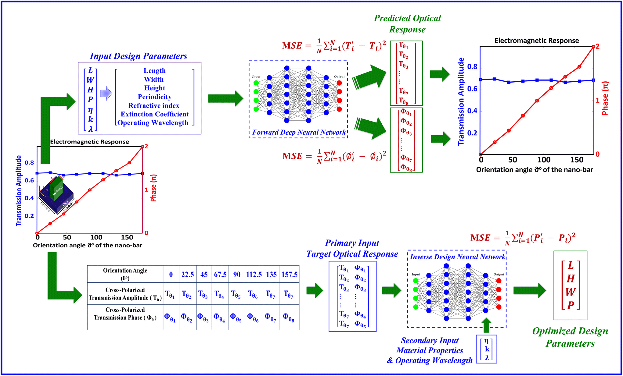 | ||
| Fig. 2 Structural outline of the proposed forward and inverse design models. | ||
The upper part of Fig. 2 shows the schematic of the proposed forward design model. Each input sample is a [7 × 1] vector containing L, W, H, P, n, k, and λ of the corresponding unit cell. Apart from n and k which are dimensionless quantities, all the other features are measured in nanometers. The forward neural network is separately trained for transmission amplitude and phase. Input parameters are the same in both the cases whereas the output labels are 1D arrays of size [8 × 1], representing amplitude samples at distinct orientation angles of the bar, i.e., [Aθ1, Aθ2,...., Aθ8], for transmission amplitude training and the phase samples at distinct orientation angles of the bar, i.e., [ϕθ1,ϕθ2,....,ϕθ8], for transmission phase training, respectively. Here the problem at hand is a regression problem. Typically, a regression task involves predicting a single numeric value but here we need to predict more than one numeric value with two different categories (A and ϕ) so this problem is referred to as multiple-output regression. Therefore we have designed a multi-input multi-output regression based forward deep neural network whose detailed architecture is shown in Fig. 3(a). The proposed network contains six fully connected hidden layers with Leaky ReLU (Leaky Rectified linear unit) as the non-linear activation function. First three hidden layers perform up-sampling to explore maximum linear combinations and extract maximum information from the input, whereas the rest of the hidden layers perform down-sampling to keep only the important information and map it to the output. Different numbers of layers and the number of neurons per layer were tried before finalizing the proposed architecture.
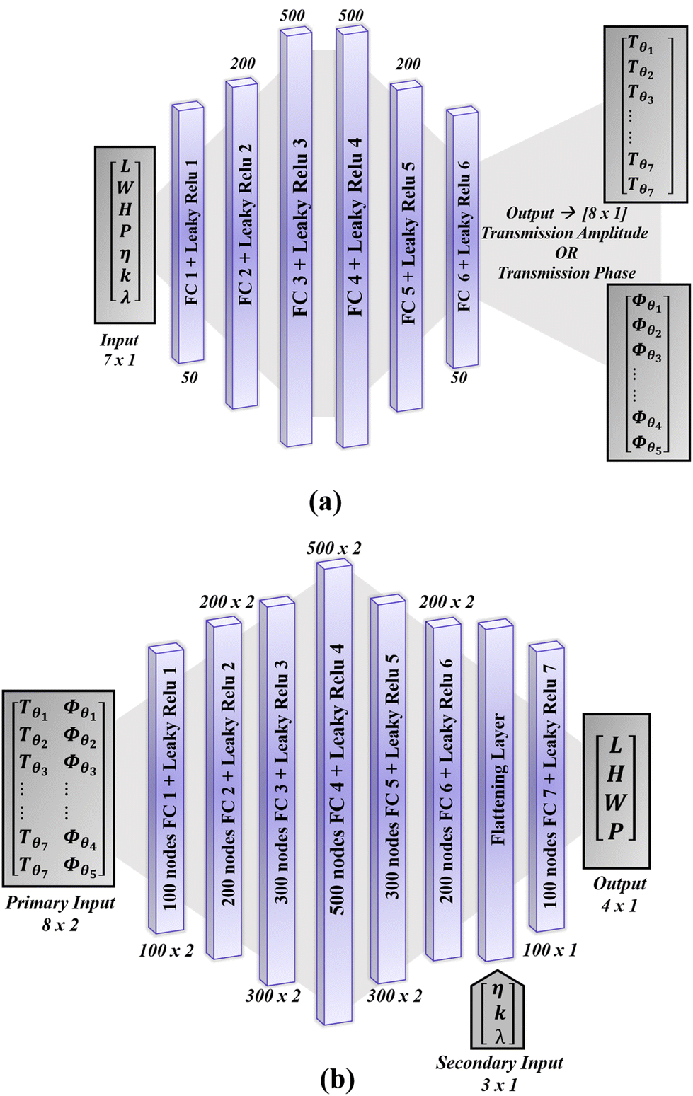 | ||
| Fig. 3 Detailed architecture of (a) forward predicting neural networks. The architecture consists of six hidden layers, the number of neurons per layer and the non-linear activation function of each layer are mentioned within the layer. Two forward networks with the same architecture are separately trained, one for the transmission amplitude predictions and other for the phase predictions, respectively. (b) Inverse design neural network. It consists of 7 hidden FC layers and a flattening layer before the last hidden layer. The number of neurons per layers and their activation function are mentioned within the layers, whereas the labels 100 × 2, 200 × 2, etc. show the volume of each layer. | ||
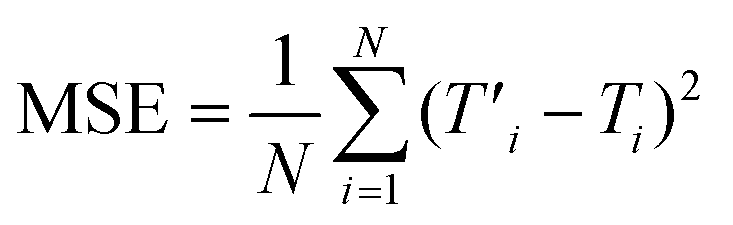
The forward predicting neural network is trained using a Nesterov Adam optimizer with a learning rate of 10−3 to minimize the loss function between the label transmission amplitude (T) or phase (ϕ) and the predicted transmission amplitude (T′) or phase (ϕ′). Since we are dealing with a regression problem, the loss function here is defined as the mean squared error (MSE) between T and T′, and ϕ and ϕ′:
 | (2) |
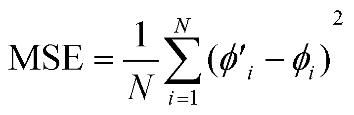 | (3) |
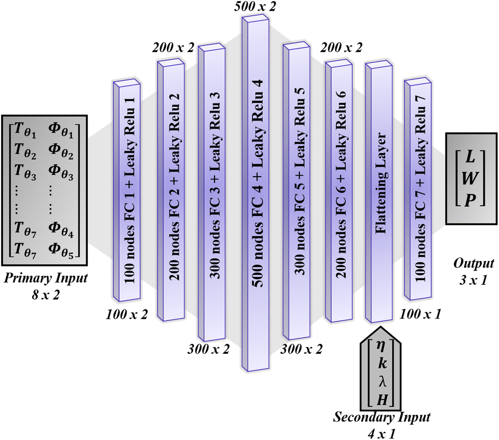
The lower part of Fig. 2 shows the schematic of the proposed inverse design model which is our eminent contribution to provide an optimization tool for the nanostructures to achieve the desired optical response. For the inverse model, the desired transmission amplitude and phase at eight distinct orientation angles of the nano-bar will be fed as the primary input to the model, whereas the refractive index and extinction coefficient of the material we want to use and the desired operating wavelength are fed as the second input to the model. As a result, the network will provide the optimized structural parameters i.e., L, W, H, and P to achieve the desired response. Mathematically the inverse problem can be expressed as:
| [L, W, H, P] = fn,k,λ[ϕ,Amp] | (4) |
The detailed architecture of the proposed multi-input multi-output regression based inverse design neural network is shown in Fig. 3(b). This neural network consists of seven hidden layers with a Leaky ReLU activation layer with α = 0.1. Since the input here is multi-dimensional, after 6 six hidden layers, a flattening layer is applied, followed by batch normalization layers, and the resulting 1D array is concatenated with a second input array. The second input contains three features which are the refractive index (n), extinction coefficient (k), and operating wavelength (λ). Each of these input features is independently normalized by subtracting its respective mean from all the samples and dividing by its variance. Thus, we have an array with normalized features for concatenation.
The inverse design network is trained using a Nesterov Adam optimizer with a learning rate of 10−3 to minimize the loss function between the set of label structural parameters (P) and the predicted structural parameters (P′). Since we are dealing with a regression problem, so the loss function here is defined as the mean squared error (MSE) between P and P′:
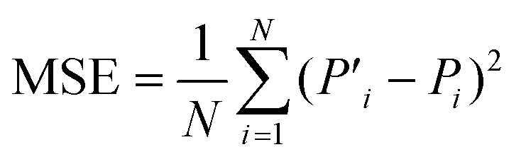 | (5) |
We have kept the model as simple as possible to avoid any additional complexity and make it usable for the researchers belonging to the field of optics and photonics having minimum expertise in the field of deep learning.
2.1 Dataset collection
For the forward predicting neural network, the datasets are defined as DFA = [(XFi, YFAi), i = 0,1,2,....,N] and DFϕ=[(XFi, YFϕi), i = 0,1,2,....,N] for amplitude and phase training, respectively. Here the input XFi remains the same for both amplitude and phase datasets, and it is defined as XFi = [Li, Wi, Hi, Pi, ni, ki, λi]. XFi represents a [7 × 1] feature vector of the ith data sample and N is the total number of samples. As mentioned earlier, six different dielectric materials and six different operating wavelengths are used while collecting the dataset. For each material i.e., each pair of n and k, the geometrical parameters are varied in the following range:• Length of the nano-bar (L): 100–400 nm
• Width of the nano-bar (W): 80–350 nm
• Periodicity of the nano-bar (P): 250–500 nm
• Height of the nano-bar (H): 100–400 nm for low aspect ratio materials, i.e., a-Si:H, and modified phosphorus doped a-Si:H, Si3N4, and 500–1000 nm for high aspect ratio materials, i.e., TiO2, GaP and GaN.
• Orientation of the nano-bar (θ): 0°–180°, and step size: 22.5°
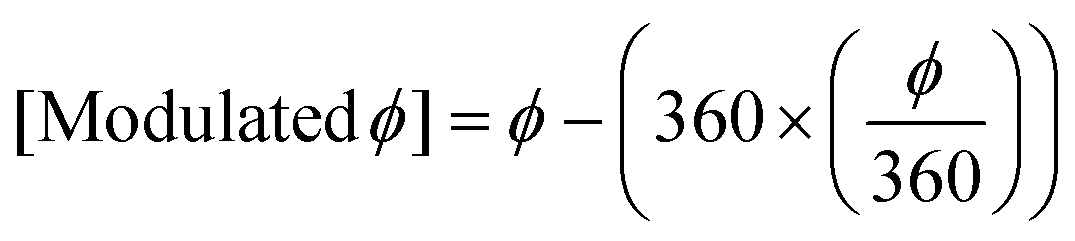
Different combinations of different values of the nano-bar's geometrical parameters (within the mentioned ranges) are simulated to collect a dataset having enough variance. The process is repeated for each of the six wavelengths selected from the visible regime i.e., 633 nm – red, 600 nm – orange, 580 nm – yellow, 550 nm – green, 480 nm – blue, and 404 nm – violet. All the simulations are carried out with circularly polarized incident light and periodic boundary conditions. The resulting cross-polarized transmission amplitude and phase at the given wavelength are stored as the output labels YFi at eight distinct orientation angles of the ith nano-bar sample under consideration. Thus YFAi = [Ai,θ1,Ai,θ2,....,Ai,θ8] for amplitude training and YFϕi = [ϕi,θ1,ϕi,θ2,....,ϕi,θ8] for phase training. The phase angles are modulated by 360° to convert negative angles into positive angles to avoid dead neurons. This modulation is performed using the following equation:
 | (6) |
Overall, YFAi and YFϕi are the arrays of size [8 × 1] each, where the 8 rows represent 8 definite orientations i.e., θ = 0°, 22.5°, 45°, 67.5°, 90°, 112.5°, 135°, and 157.5°.
The forward neural network model is trained using the optimization function f(XFi, YFi; w) parameterized by w, where w is a matrix of weights controlling the function's mapping and is optimized to precisely fit the training data while avoiding overfitting and maintaining generalizability for the test data. L2 regularization is used to avoid overfitting. For the inverse design neural network, the dataset is defined as DI = [(XIj, MIj, YIj), j = 0,1,2,....,N] where the primary input labels XIj represent the target cross-polarization transmission amplitude and the phase of the jth data sample, and it is the same as the forward dataset's combined output labels i.e., XIj = [AIj and ϕIj ] where AIj = [Aj,θ1,Aj,θ2,....,Aj,θ8] and ϕIj = [ϕj,θ1,ϕj,θ2,....,ϕj,θ8]. Thus XIj is an array of size [8 × 2], where the 8 rows represent 8 definite orientations and 2 columns represent the amplitude and phase. The second input MIj is a [3 × 1] array, which represents the refractive index (n), extinction co-efficient (k) and the operating wavelength (λ). The output of the inverse design network is the most optimum set of geometrical parameters which will generate the target optical response given at the primary input, with the material and operating wavelength specified by the second input n, k and λ. Therefore, the output labels YIj = [Lj, Wj, Hj, Pj] are a set of [4 × 1] geometrical parameters of the jth unit cell sample. The inverse neural network model is trained using the optimization function f([XIj, MIj], YIj; w) parameterized by w, where w is a matrix of weights controlling the function's mapping and is optimized to precisely fit the training data while avoiding overfitting and maintaining generalizability for the test data.
2.2 Inverse design with fabrication constraints
The inverse design procedure of metasurfaces also suffers from some practical fabrication constraints. The fabrication of metasurfaces is a very expensive procedure, requires high-end machinery, and needs to be performed with great expertise and exactitude. Therefore its fabrication constraints are mandatory to be kept in mind to avoid recurring fabrications of the same device. Among these constraints, the aspect ratio of the nano-resonators is the most crucial parameter. An aspect ratio which is defined as the ratio of the height to the smallest feature of the nano-resonator directly depends upon the height of the nano-resonator. A larger height means a higher aspect ratio, which means more material usage, more fabrication complexity, and more expense. Also, the height should not be too low that it becomes impossible to prepare. Therefore, we fix the height of the nano-bar for each material. The height must remain the same regardless of the operating wavelength to prepare broadband visible regime meta devices. The optical constants n and k of the thin films also vary with the height, so fixing the height according to our fabrication equipment and its limitations will fix the n and k too for a certain wavelength. In this way, we can feed very precise values of n and k measured via ellipsometry by depositing thin films of the specific height that we have fixed for each material. This can lead to a good agreement between the measured and the simulated results.Therefore, some modification is made to the input and output labels of the proposed inverse design neural network to cater to the aforementioned limitations. The number of the nano-bar's geometrical parameters to be optimized is now reduced to three, i.e., L, W, and P, instead of four as the height is now fixed for each material (Table 3) and eliminated from the parameters that need to be tuned. The primary input of the inverse design network shown in Fig. 2 and Fig. 3(b) remains the same, whereas the secondary input now contains four parameters, i.e., n, k, λ, and H (height fixed). The geometrical parameters of the bar to be optimized, i.e., the output labels now contain the length, width, and periodicity only. Fig. 4 shows the fabrication-inspired inverse design neural network as explained here. The dataset for this network is collected in the same way as described previously, but its definition is somewhat changed now. The inverse dataset is now defined as DI = [(XIj, MIj, YIj), j = 0,1,2,....,N] where the primary input labels, i.e., XIj = [[Aj,θ1,Aj,θ2,....,Aj,θ8] and [ϕj,θ1,ϕj,θ2,....,ϕj,θ8] ], are a set of arrays of size [8 × 2], where the 8 rows represent 8 definite orientations and 2 columns represent the amplitude and phase. The secondary input MIj = [n, k, H, λ] is a [4 × 1] array, which represents the refractive index (n), extinction co-efficient (k), operating wavelength (λ) and height (H). The output of the inverse design network is the most optimum set of geometrical parameters which will generate the target optical response given at the primary input, with the material specified by the secondary inputs n, k, and H and the operating wavelength also specified by the secondary input. Therefore, the output labels YIj = [Lj, Wj, Pj] are a set of [3 × 1] geometrical parameters of the jth unit-cell sample. This inverse neural network model is again trained using the same optimization function f([XIj, MIj], YIj; w) parameterized by w, where w is a matrix of weights controlling the function's mapping and is optimized to precisely fit the training data while avoiding overfitting and maintaining generalizability for the test data.
| Material | a-Si:H |
TiO2 | GaN | GaP | Si3N4 | Modified a-Si:H |
|---|---|---|---|---|---|---|
| Fixed height (nm) | 400 | 600 | 600 | 600 | 450 | 400 |
 | ||
| Fig. 4 Detailed architecture of the fabrication inspired inverse design neural network. The secondary input now contains the fixed height as a new parameter which is eliminated from the output now. | ||
3 Results and discussion
3.1 Forward predicting neural network
The forward predicting neural network is trained using a Nesterov Adam optimizer with a learning rate of 10−3 to minimize the mean square error loss functions given by eqn (2) and eqn (3) for transmission amplitude and phase, respectively. The model is trained optimally in 500 epochs with a batch size of 32. The average MSE achieved while training is 7.3 × 10⁻⁴. A detailed statistical analysis of the MSE over the test dataset (over 300 samples) is shown in Fig. 5. This analysis shows that the trained model exhibits a quite low distribution of errors over the test dataset and the average MSE is 1.8 × 10⁻³. The simulated and the DL model predicted results for some random test samples are shown in Fig. 6 and 7.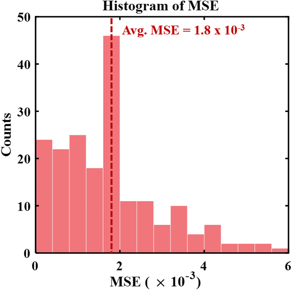 | ||
| Fig. 5 Statistical analysis of MSE over the test dataset (for the forward trained model). This MSE histogram shows that 96% of the test samples have an MSE <4.2 × 10⁻³. | ||
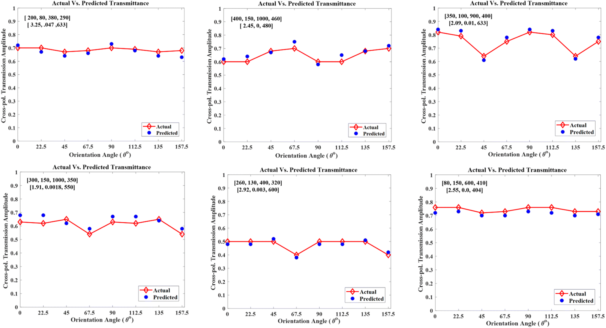 | ||
| Fig. 6 Comparative analysis of the cross-polarized transmission amplitude achieved via simulations and DL model predictions. Here the red line represents the simulated transmittance amplitude, whereas the blue dots represent the proposed model predicted transmittance amplitude. Geometrical parameters of the corresponding unit cells and the material properties along with the operating wavelengths are shown in the top right insets in the following sequence: [length, width, height, periodicity] and [refractive index, extinction coefficient, lambda]. All these samples, randomly selected from the test dataset, show a good agreement between the simulated and the predicted transmittance phases. | ||
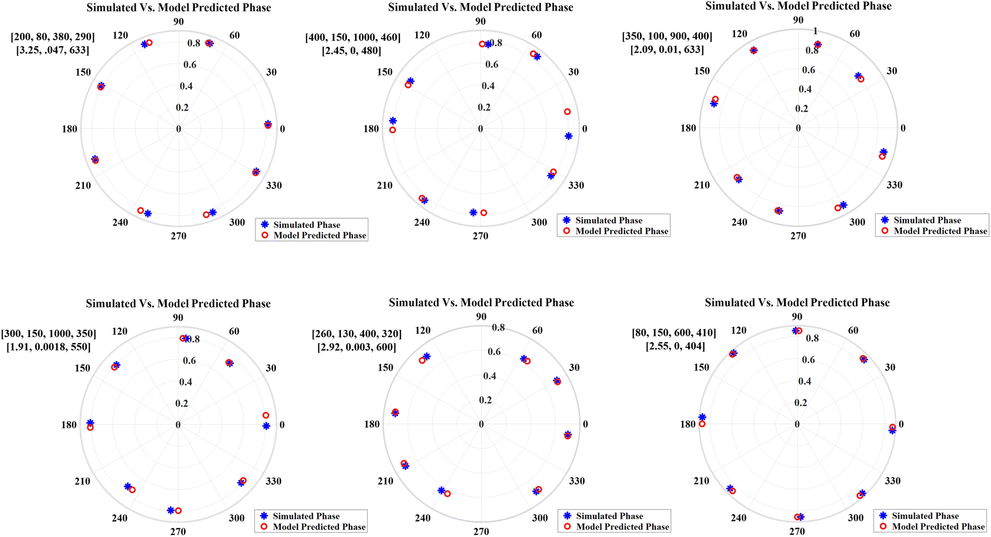 | ||
| Fig. 7 Comparative analysis of the cross-polarized transmission phase achieved via simulations and DL model predictions. Here the blue star symbols represent the simulated transmittance phase angles, whereas the red hole symbols represent the proposed model predicted transmittance angles. Geometrical parameters of the corresponding unit cells and the material properties along with the operating wavelengths are shown in the top right insets in the following sequence: [length, width, height, periodicity] and [refractive index, extinction coefficient, lambda]. All these samples, randomly selected from the test dataset, show a good agreement between the simulated and the predicted transmittance phases. | ||
Fig. 5 shows the statistical histogram of the MSE between the predicted and the simulated transmission amplitude of the test dataset samples. It can be seen that the average mean square error is 1.8 × 10⁻³, whereas 99% of the data exhibits an MSE less than 6 × 10⁻³ and 96% of the data exhibits an MSE <4.2 × 10⁻³.
To analyze the prediction accuracy of the trained forward predicting neural networks, transmittance amplitude and phase predictions of some random test data samples and their comparison with the simulated transmittance are shown in Fig. 6 (amplitude) and Fig. 7 (phase), respectively. The structural parameters, operating wavelength, and material properties of the corresponding nano bar unit cells are mentioned in the insets in the sequence listed in the captions. These unit cells are constructed in CST and simulated with circularly polarized incident light and periodic boundary conditions. The resulting cross-polarized transmission amplitude and phase at the given wavelength is taken as the simulated response. The test samples shown in these figures are selected at random for different operating wavelengths and materials to show the diversity of the trained model. These samples show excellent coherence between the numerical simulations and the forward neural network predicted results for both the amplitude and phase at all the orientation angles under consideration.
3.2 Inverse design neural network
The inverse design neural network serves as an optimization tool providing optimal geometrical parameters to achieve the desired transmission response. It is trained using a Nesterov Adam optimizer with a learning rate of 10−3 to minimize the loss function given by eqn (5). The model is trained optimally in 1000 epochs with a batch size of 32. The average MSE achieved while training is 1.1. The evaluation of the trained inverse model over the test dataset shows that it gives excellent predictions and the average MSE for the test dataset is 2.8 × 10⁻¹. The comparative analysis of the label and the DL model predicted geometrical parameters for some random test samples is shown in Fig. 8. Here, the primary input target response is maximum cross-polarized transmission amplitude and full phase coverage. The material properties and the operating wavelength which are given as the second input are listed in the corresponding insets for each sample in Fig. 8. These samples are randomly selected for different operating wavelengths and materials to show the diversity of the trained model. The comparison between the label and the predicted parameters show excellent coherence validating the accurate performance of the inverse design network. Thus, the proposed inverse design model is a generalized model that can be used to optimize a bar shaped unit cell for different dielectric materials and wavelengths in the visible regime. It eliminates the need for conventional EM software, in which we need to execute the lengthy optimization procedure from scratch for each different material and wavelength.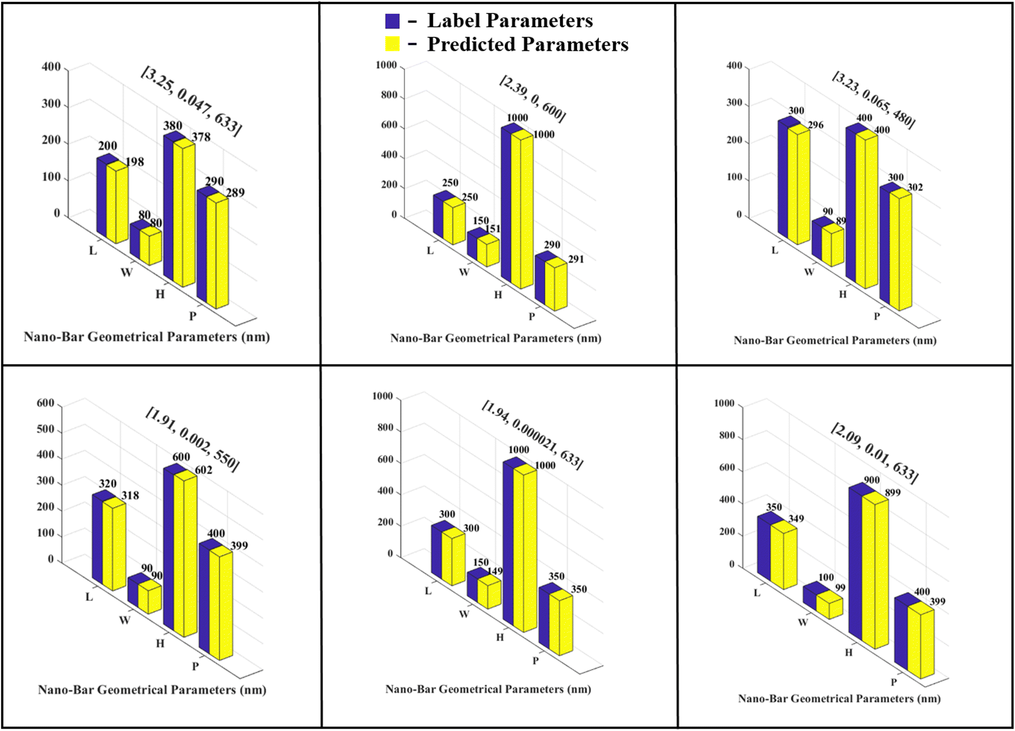 | ||
| Fig. 8 Comparative analysis of the predicted and the simulated geometric parameters of some random test samples. Here the blue bars represent the label (simulated) geometrical parameters, whereas the yellow bars represent the proposed model predicted parameters. The corresponding material properties and the operating wavelengths are shown in the top insets in the following sequence: [refractive index, extinction coefficient, lambda]. All these samples, randomly selected from the test dataset show a very good agreement between the label and the predicted parameters. | ||
Table 4 shows the individual average MSEs for each material in terms of forward predictions and inverse design optimization. This table shows that the trained forward models exhibit quite a low distribution of errors for all the materials (irrespective of the operating wavelength). For forward amplitude predictions, the average MSE of all the materials is less than 5.5 × 10⁻³; the MSE of Si3N4 is slightly higher than those of others because it is an unseen material that is not a part of the training dataset. For forward phase predictions, the average MSE of Si3N4 is 9.7 × 10⁻¹, whereas all the other materials have average MSEs in the order of 10–2 and 10–3. Since the inverse design is more challenging due to its one to many mapping issue, the MSEs are comparatively higher. For the inverse predictions of optimum parameters, the average MSE of the unseen material Si3N4 is 1.24, whereas the average MSE of the rest of the materials is in the orders of 10–1 and 10–2. These MSEs can be further reduced by collecting more datasets for each material. Table 4 validates the capacity of the proposed model to effectively work for multiple materials.
| Material | a-Si:H |
TiO2 | GaN | GaP | Mod. a-Si:H |
Si3N4 |
|---|---|---|---|---|---|---|
| Avg. MSE for forward amplitude predictions | l.89 × 10−4 | 1.3 × 10⁻⁴ | 3.2 × 10⁻³ | 1 × 10⁻³ | 1.1 × 10⁻⁴ | 5.5 × 10⁻³ |
| Avg. MSE for forward phase predictions | 2.24 × 10⁻³ | 5.2 × 10⁻² | 4.3 × 10⁻² | 6.7 × 10⁻² | l.44 × 10−3 | 9.7 × 10⁻² |
| Avg. MSE for inverse design parameter predictions | 0.087 | 0.105 | 0.104 | 0.104 | 0.09 | l. 24 |
To further validate the performance of the inverse design network, we simulated the parameters predicted for some random samples in Fig. 8 and compared the transmission response given by the predicted parameters to that given by the ground truth parameters. All the simulations are performed using the standard solver settings used while extracting the dataset. This comparison, shown in Fig. 9, depicts that the predicted parameters perfectly achieve the desired target when simulated in the traditional solver. Therefore, the proposed inverse design network once trained can be used as an optimization tool to obtain optimal parameters for our design target within a fraction of seconds.
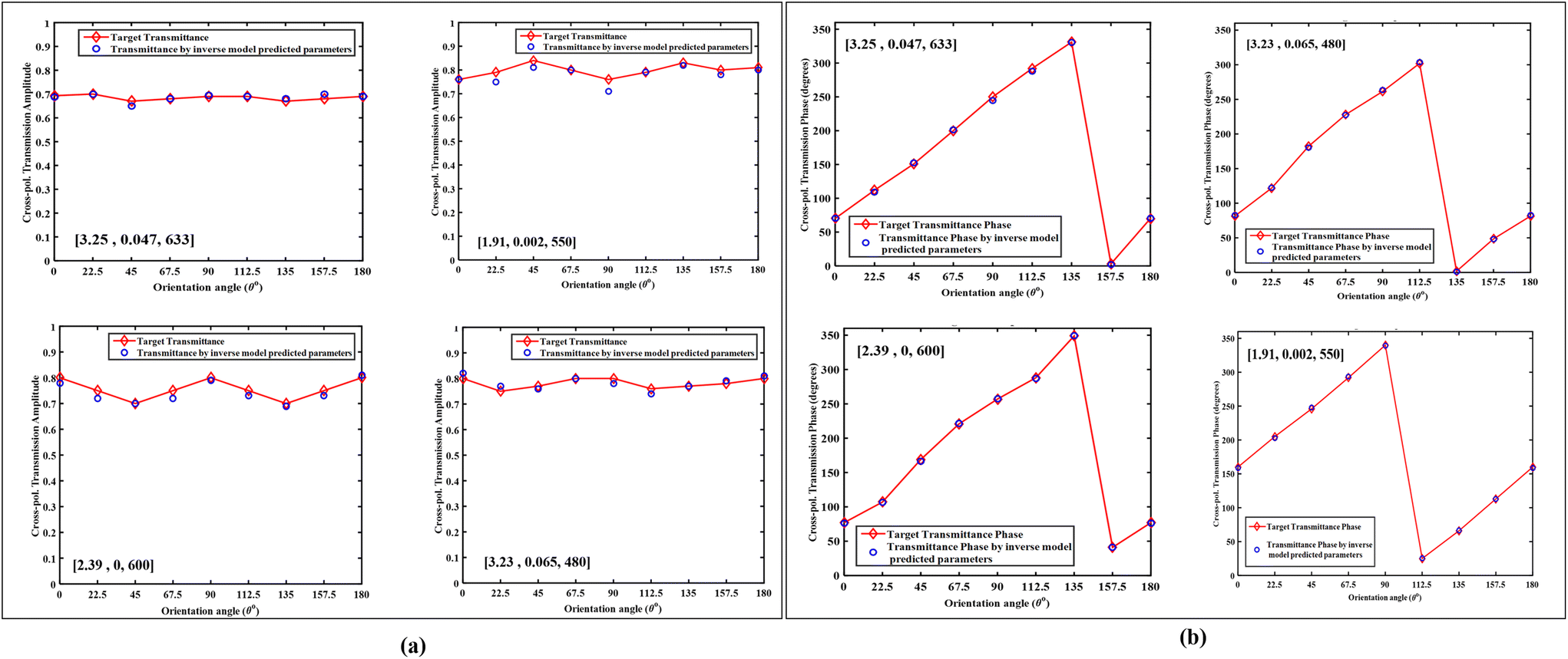 | ||
| Fig. 9 Comparative analysis of the target transmission amplitude and phase with the transmission amplitude and phase given by the predicted design parameters. (a) The red line shows the target amplitude and the blue holes represent the simulated amplitude by the predicted parameters. The corresponding material properties and the operating wavelengths are given insets listed as [refractive index, extinction coefficient, lambda]. (b) The red line shows the target phases and the blue holes represent the simulated phases by the predicted parameters. The corresponding material properties and the operating wavelengths are given as insets in the following sequence: [refractive index, extinction coefficient, lambda]. | ||
3.3 Comparison of optimization performed by the inverse design neural network and traditional CST microwave studio optimization tools
Some common and widely used traditional optimization tools in commercial software like CST MICROWAVE STUDIO®† are trust region framework, genetic algorithm, and particle swarm optimization (PSO). We have compared the performance of our inverse design-based optimization with these optimization tools with respect to the number of optimization parameters, time consumption, the number of solver runs, and the accuracy achieved by each of these approaches. This comparison is presented in Table 5. All the CST optimization tools require some prior knowledge of the range of the parameters to define a search space and find the optimized values within that space to avoid directionless searching. So here, in Table 5 the maximum range refers to the size of the search space of geometric parameter values. For example, if we want to optimize the value of the period P, we will calculate an approximate value using the formula P = λ/2NA21 and then define a search space with ± 250 nm around this value. So the total range of the search space will be 500 nm. Increasing the range of the search space will increase the population of candidate solutions, thus delays the prediction of the optimum value of parameters. On the other hand, once our inverse model is trained for optimization, we can simply input the target response and obtain the optimized parameters without requiring any prior knowledge or numerical calculation of the range of parameters.| ★Features | Methods | |||
|---|---|---|---|---|
| DL model | CST optimization tools | |||
| Trust region frame work | Genetic algorithm | Particle swarm algorithm (PSO) | ||
| Prior knowledge of parameter range required? | No. | Yes | Yes | Yes |
| No. of parameters to be optimized | 4 | 4 | 4 | 4 |
| Max. range of parameters | 1000 nm | 500 nm | 500 nm | 500 run |
| Time consumed | −1.8 s | −25 min | −3 hours | −3.5 hours |
| No. of solver runs | I | −36 | −120 | −12 5 |
| Accuracy | 97% | 99% | 100% | 100% |
Table 5 also shows that the DL-based inverse design network works much faster and requires only a single run as compared to the other optimization algorithms which require more time and a lot of solver runs. Each time even if we have a slight change in the target response, the CST optimization algorithms will need to perform a large number of solver runs from scratch. The accuracy of the proposed model is also comparable to the conventional algorithm's accuracy; this accuracy is measured with respect to the target transmission and the transmission given by the predicted (optimized) parameters.
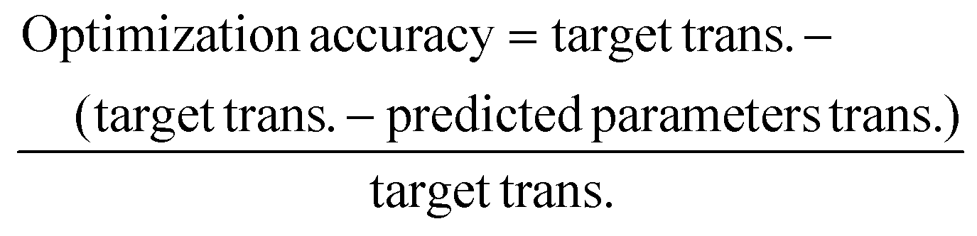 | (7) |
From Table 5, it is evident that the proposed inverse neural network optimization tool is faster than traditional optimization tools. If the number of parameters to be optimized and their range are increased, it will further increase the time consumed and the number of solver runs to provide the optimized parameters, making the traditional tools inefficient and sluggish.
4 Conclusion
This paper presents the modeling and optimization of all-dielectric transmissive metasurfaces via deep neural networks. A forward predicting multi-input multi-output regression neural network is demonstrated to accurately map the cross-polarized transmission amplitude and phase, while simultaneously taking all the geometric parameters, the material properties, and the operating wavelength of the nano-resonators as the input. The trained model predicts the transmission amplitude and phase of the bar-shaped nano-resonators at distinct orientation angles of the bar to ensure the uniformity of the amplitude regardless of the orientation and a 2π phase coverage. Results show that the trained forward model exhibits a quite low distribution of errors over the test dataset for all the materials and wavelengths and achieves an average MSE of 1.8 × 10⁻³. Thus it can replace the iterative, time-consuming, and computationally exhaustive EM simulations to evaluate the performance of a metasurface unit cell. An inverse design neural network serving as an optimization tool is also demonstrated, which takes the target electromagnetic response (both amplitude and phase), material constitutive parameters, and working wavelength as the input and provides optimized structural dimensions as the output to match the target response. The evaluation of the trained inverse model over the test dataset shows that it gives excellent predictions and the average MSE for the test dataset is 2.8 × 10⁻¹. A detailed comparison of the proposed optimization inverse design and the traditional commercial software optimization algorithms is performed. This comparison validates that the proposed deep learning based inverse optimization is faster which requires comparatively less computational power, and provides results in a single run, in contrast to traditional approaches which require lots of solver runs, memory, and computational resources.Conflicts of interest
There are no conflicts to declare.Acknowledgements
Y. M. would like to acknowledge research funding to the Innovative Technologies Laboratories from King Abdullah University of Science and Technology (KAUST).References
- C. L. Holloway, E. F. Kuester, J. A. Gordon, J. O'Hara, J. Booth and D. R. Smith, An overview of the theory and applications of metasurfaces: The two-dimensional equivalents of metamaterials, IEEE Antennas Propag. Mag., 2012, 54, 10–35 Search PubMed.
- D. Lin, P. Fan, E. Hasman and M. L. Brongersma, Dielectric gradient metasurface optical elements, Science, 2014, 345, 298–302 CrossRef CAS PubMed.
- N. Yu, P. Genevet, M. A. Kats, F. Aieta, J.-P. Tetienne, F. Capasso and Z. Gaburro, Light propagation with phase discontinuities: generalized laws of reflection and refraction, Science, 2011, 334, 333–337 CrossRef CAS PubMed.
- L. Liu, X. Zhang, M. Kenney, X. Su, N. Xu, C. Ouyang, Y. Shi, J. Han, W. Zhang and S. Zhang, Broadband metasurfaces with simultaneous control of phase and amplitude, Adv. Mater., 2014, 26, 5031–5036 CrossRef CAS PubMed.
- T. Roy, S. Zhang, I. W. Jung, M. Troccoli, F. Capasso and D. Lopez, Dynamic metasurface lens based on MEMS technology, APL Photonics, 2018, 3, 021302 CrossRef.
- A. Hosseini, H. Nejati and Y. Massoud, Design of a maximally flat optical low pass filter using plasmonic nanostrip waveguides, Opt. Express, 2007, 15, 15280–15286 CrossRef PubMed.
- A. Hosseini and Y. Massoud, Optical range microcavities and filters using multiple dielectric layers in metal-insulator-metal structures, J. Opt. Soc. Am. A, 2007, 24, 221–224 CrossRef CAS PubMed.
- Z. Jin, D. Janoschka, J. Deng, L. Ge, P. Dreher, B. Frank, G. Hu, J. Ni, Y. Yang and J. Li, et al., Phyllotaxis-inspired nanosieves with multiplexed orbital angular momentum, eLight, 2021, 1, 1–11 CrossRef.
- H. Ahmed, A. A. Rahim, H. Maab, M. M. Ali, N. Mahmood and S. Naureen, Phase engineering with all-dielectric metasurfaces for focused-optical-vortex (FOV) beams with high cross-polarization efficiency, Opt. Mater. Express, 2020, 10, 434–448 CrossRef CAS.
- M. Mehmood, S. Mei, S. Hussain, K. Huang, S. Siew, L. Zhang, T. Zhang, X. Ling, H. Liu and J. Teng, et al., Visible-frequency metasurface for structuring and spatially multiplexing optical vortices, Adv. Mater., 2016, 28, 2533–2539 CrossRef CAS PubMed.
- M. A. Ansari, I. Kim, I. D. Rukhlenko, M. Zubair, S. Yerci, T. Tauqeer, M. Q. Mehmood and J. Rho, Engineering spin and antiferromagnetic resonances to realize an efficient direction-multiplexed visible meta-hologram, Nanoscale Horiz., 2020, 5, 57–64 RSC.
- M. A. Ansari, I. Kim, D. Lee, M. H. Waseem, M. Zubair, N. Mahmood, T. Badloe, S. Yerci, T. Tauqeer and M. Q. Mehmood, et al., A spin-encoded all-dielectric metahologram for visible light, Laser Photonics Rev., 2019, 13, 1900065 CrossRef.
- M. A. Naveed, J. Kim, I. Javed, M. A. Ansari, J. Seong, Y. Massoud, T. Badloe, I. Kim, K. Riaz and M. Zubair, et al., Novel Spin-Decoupling Strategy in Liquid Crystal-Integrated Metasurfaces for Interactive Metadisplays, Adv. Opt. Mater., 2022, 2200196 CrossRef CAS.
- A. S. Rana, M. Q. Mehmood, H. Jeong, I. Kim and J. Rho, Tungsten-based ultrathin absorber for visible regime, Sci. Rep., 2018, 8, 1–8 CAS.
- A. S. Rana, M. Zubair, A. Danner and M. Q. Mehmood, Revisiting tantalum based nanostructures for efficient harvesting of solar radiation in STPV systems, Nano Energy, 2021, 80, 105520 CrossRef CAS.
- S. Ijaz, A. S. Rana, Z. Ahmad, B. Rehman, M. Zubair and M. Q. Mehmood, Exploiting zirconium nitride for an efficient heat-resistant absorber and emitter pair for solar thermophotovoltaic systems, Opt. Express, 2021, 29, 31537–31548 CrossRef CAS PubMed.
- M. A. Abbas, J. Kim, A. S. Rana, I. Kim, B. Rehman, Z. Ahmad, Y. Massoud, J. Seong, T. Badloe and K. Park, et al., Nanostructured chromium-based broadband absorbers and emitters to realize thermally stable solar thermophotovoltaic systems, Nanoscale, 2022, 14, 6425–6436 RSC.
- H. S. Khaliq, K. Riaz, M. Zubair, M. A. Ansari, M. R. Akram, T. Naeem, J. Zhang, W. Zhu, D. Zhang and X. Wang, et al., Metamaterials XII, 2020, p. 113441N Search PubMed.
- Y. Luo, Y. Zhao, J. Li, E. Çetintaş, Y. Rivenson, M. Jarrahi and A. Ozcan, Computational imaging without a computer: seeing through random diffusers at the speed of light, eLight, 2022, 2, 1–16 CrossRef.
- S. Noureen, H. Ahmed, N. Mahmood, M. Zubair and M. Q. Mehmood, Nanoengineering: Fabrication, Properties, Optics, Thin Films, and Devices XVII, 2020, p. 1146706.
- N. Mahmood, H. Jeong, I. Kim, M. Q. Mehmood, M. Zubair, A. Akbar, M. Saleem, M. S. Anwar, F. A. Tahir and J. Rho, Twisted non-diffracting beams through all dielectric meta-axicons, Nanoscale, 2019, 11, 20571–20578 RSC.
- S. Jahani and Z. Jacob, All-dielectric metamaterials, Nat. Nanotechnol., 2016, 11, 23–36 CrossRef CAS PubMed.
- A. Arbabi, Y. Horie, M. Bagheri and A. Faraon, Dielectric metasurfaces for complete control of phase and polarization with subwavelength spatial resolution and high transmission, Nat. Nanotechnol., 2015, 10, 937–943 CrossRef CAS PubMed.
- H. Ahmed, S. Noureen, N. Mahmood, A. Rahim, M. M. Ali, H. Maab and M. Q. Mehmood, 2020 17th International Bhurban Conference on Applied Sciences and Technology (IBCAST), 2020, pp. 12–15.
- X. Ming, X. Liu, L. Sun and W. J. Padilla, Degenerate critical coupling in all-dielectric metasurface absorbers, Opt. Express, 2017, 25, 24658–24669 CrossRef CAS PubMed.
- M. Alam and Y. Massoud, RLC ladder model for scattering in single metallic nanoparticles, IEEE Trans. Nanotechnol., 2006, 5, 491–498 Search PubMed.
- A. Hosseini, A. Nieuwoudt and Y. Massoud, Efficient simulation of subwavelength plasmonic waveguides using implicitly restarted Arnoldi, Opt. Express, 2006, 14, 7291–7298 CrossRef PubMed.
- M. Alam and Y. Massoud, 48th Midwest Symposium on Circuits and Systems, 2005, 2005, pp. 1928–1931.
- M. Alam and Y. Massoud, A closed-form analytical model for single nanoshells, IEEE Trans. Nanotechnol., 2006, 5, 265–272 Search PubMed.
- B. A. Slovick, Z. G. Yu and S. Krishnamurthy, Generalized effective-medium theory for metamaterials, Phys. Rev. B: Condens. Matter Mater. Phys., 2014, 89, 155118 CrossRef.
- L. Lewin, The electrical constants of a material loaded with spherical particles, Proc. Inst. Electr. Eng., Part 3, 1947, 94, 65–68 Search PubMed.
- X. Chang, L. Bian and J. Zhang, Large-scale phase retrieval, eLight, 2021, 1, 1–12 CrossRef.
- A. S. Lundervold and A. Lundervold, An overview of deep learning in medical imaging focusing on MRI, Z. Med. Phys., 2019, 29, 102–127 CrossRef PubMed.
- Z. Chen and M. Segev, Highlighting photonics: looking into the next decade, eLight, 2021, 1, 1–12 CrossRef.
- I. Sajedian, T. Badloe and J. Rho, Optimisation of colour generation from dielectric nanostructures using reinforcement learning, Opt. Express, 2019, 27, 5874–5883 CrossRef CAS PubMed.
- I. Malkiel, M. Mrejen, A. Nagler, U. Arieli, L. Wolf and H. Suchowski, Plasmonic nanostructure design and characterization via deep learning, Light: Sci. Appl., 2018, 7, 1–8 CrossRef CAS PubMed.
- S. Noureen, M. Zubair, M. Ali and M. Q. Mehmood, 2021 International Bhurban Conference on Applied Sciences and Technologies (IBCAST), 2021, pp. 289–292.
- L. Li, H. Zhao, C. Liu, L. Li and T. J. Cui, Intelligent metasurfaces: control, communication and computing, eLight, 2022, 2, 1–24 CrossRef.
- C. C. Nadell, B. Huang, J. M. Malof and W. J. Padilla, Deep learning for accelerated all-dielectric metasurface design, Opt. Express, 2019, 27, 27523–27535 CrossRef CAS PubMed.
- S. Noureen, M. Zubair, M. Ali and M. Q. Mehmood, Deep learning based hybrid sequence modeling for optical response retrieval in metasurfaces for STPV applications, Opt. Mater. Express, 2021, 11, 3178–3193 CrossRef CAS.
- A. Mall, A. Patil, A. Sethi and A. Kumar, A cyclical deep learning based framework for simultaneous inverse and forward design of nanophotonic metasurfaces, Sci. Rep., 2020, 10, 1–12 CrossRef PubMed.
- S. So and J. Rho, Designing nanophotonic structures using conditional deep convolutional generative adversarial networks, Nanophotonics, 2019, 8, 1255–1261 Search PubMed.
- S. An, B. Zheng, H. Tang, M. Y. Shalaginov, L. Zhou, H. Li, M. Kang, K. A. Richardson, T. Gu and J. Hu, et al., Multifunctional metasurface design with a generative adversarial network, Adv. Opt. Mater., 2021, 9, 2001433 CrossRef CAS.
- L. S. Neto, J. Dickmann and S. Kroker, Deep learning assisted design of high reflectivity metamirrors, Opt. Express, 2022, 30, 986–994 CrossRef CAS PubMed.
- I. Tanriover, W. Hadibrata and K. Aydin, Physics-based approach for a neural networks enabled design of all-dielectric metasurfaces, ACS Photonics, 2020, 7, 1957–1964 CrossRef CAS.
- S. An, C. Fowler, B. Zheng, M. Y. Shalaginov, H. Tang, H. Li, L. Zhou, J. Ding, A. M. Agarwal, C. Rivero-Baleine, et al., A novel modeling approach for all-dielectric metasurfaces using deep neural networks, arXiv preprint arXiv:1906.03387, 2019.
Footnote |
| † https://www.3ds.com/products-services/simulia/products/cst-studio-suite/. |
| This journal is © The Royal Society of Chemistry 2022 |