
 Open Access Article
 This Open Access Article is licensed under a
 Creative Commons Attribution 3.0 Unported Licence
Challenges of grazing emission X-ray fluorescence (GEXRF) for the characterization of advanced nanostructured surfaces
Dieter
Skroblin
 *a,
Analía
Fernández Herrero
a,
Thomas
Siefke
b,
Konstantin
Nikolaev
c,
Anna
Andrle
a,
Philipp
Hönicke
a,
Yves
Kayser
a,
Michael
Krumrey
a,
Christian
Gollwitzer
a and
Victor
Soltwisch
a
*a,
Analía
Fernández Herrero
a,
Thomas
Siefke
b,
Konstantin
Nikolaev
c,
Anna
Andrle
a,
Philipp
Hönicke
a,
Yves
Kayser
a,
Michael
Krumrey
a,
Christian
Gollwitzer
a and
Victor
Soltwisch
a
aPhysikalisch-Technische Bundesanstalt (PTB), Abbestraße 2–12, 10587 Berlin, Germany. E-mail: dieter.skroblin@ptb.de
bFriedrich Schiller Universität Jena, Albert-Einstein-Strasse 15, 07745 Jena, Germany
cKurchatov Institute, Kurchatov Sq 1, 123182 Moscow, Russia
First published on 13th October 2022
Abstract
The grazing emission X-ray fluorescence (GEXRF) technique offers a promising approach to determining the spatial distribution of various chemical elements in nanostructures. In this paper, we present a comparison with grazing incidence small-angle X-ray scattering (GISAXS), an established method for dimensional nanometrology, on periodic TiO2 nanostructures fabricated by a self-aligned double patterning (SADP) process. We further test the potential of GEXRF for process control in the presence of residual chromium on the structures. The angle-resolved fluorescence emission as well as the scattered radiation from the surface are collected with photon-counting hybrid pixel area detectors using scanning-free detection schemes. By modelling the X-ray standing wave (XSW) field in the vicinity of and inside the nanostructure, it is possible to obtain both the angle-resolved fluorescence intensities and the far-field scattering intensities from the same model. The comparison also illustrates that for ensemble photon-based measurement methods, accounting for roughness effects and imperfections can be essential when modelling advanced nanostructured surfaces.
1. Introduction
The development of tools for the accurate measurement of nanostructure dimensions is still a challenge in metrology.1 Electron microscopy-based techniques such as scanning electron microscopy (SEM)2 or transmission electron microscopy (TEM)3 and atomic force microscopy (AFM) are well established but have certain limitations.4,5 Some require sample destruction and can only analyse a small fraction of the sample in a finite amount of time. AFM requires a small width tip capable of penetrating very narrow grooves. Given the ever-shrinking structure sizes, this becomes an increasingly limiting factor that renders AFM unusable for the latest semiconductor gratings. Photon-based scattering techniques have the advantage that they are non-destructive, enable relatively fast measurement, and provide quite a high level of statistical accuracy.6 However, the structure sizes of current nanostructures already require probing radiation wavelengths in the EUV or X-ray spectral range due to the resolution limit. Short wavelengths, such as those used in the GISAXS technique,7,8 also require very shallow incident angles close to the critical angle of total external reflection (typically below 1°) to obtain sufficient measurable scattering from the surface.9,10 Unfortunately, this also implies that the footprint of the probing X-rays along the incidence direction on the studied sample surface is relatively long.11 Depending on the application, this can be an advantage by providing surface sensitivity and sampling statistics, or a significant disadvantage if the measurement fields to be examined are very small. This is often the case for samples in EUV lithography, where area consumption is directly related to cost. Besides the shrinking structure sizes, the steadily increasing complexity of the architectures and materials is pushing existing metrological techniques to their limits.6In addition to elastic scattering, X-rays can excite core level electrons at photon energies above the ionization threshold of the atoms. Upon filling the vacancies created in the electronic structure, X-ray fluorescence (XRF) can be emitted. One advantage of such fluorescence-based methods is their element sensitivity. Although this emission is isotropic, the interference of incident and reflected radiation produces an X-ray standing wave (XSW) field when the angle of incidence is small and the surface is flat and smooth. This gives rise to an incident angle- and energy-dependent variation of the fluorescence signal, which is used in grazing incidence X-ray fluorescence (GIXRF).12 The small incidence angle implies the same disadvantages as with GISAXS.
The GIXRF technique can also be modified by exchanging the beam paths for the excitation and detection of X-ray fluorescence.13 The sample is then illuminated perpendicularly, and the emerging fluorescence radiation is detected at a grazing emission angle. This technique is called grazing emission X-ray fluorescence (GEXRF) and is well known for characterizing unstructured thin-film systems.13–16 In those systems, refraction of the outgoing XRF radiation at interfaces can lead to interference effects in the intensity distribution. These effects have recently been used to characterize structured surfaces as well.17 A significant advantage of this method is that buried structures can also be measured due to the penetration depth of the X-rays, and the beam size alone determines the probed area in its lateral dimensions. This also enables the scanning of laterally inhomogeneous samples. In X-ray scattering experiments, the beam must be very well collimated and have low divergence, and monochromatic excitation is usually advantageous for data analysis as well.18 GEXRF measures the interference of fluorescence photons; the beam properties of the incident excitation radiation are less important. A higher divergence (resulting, for example, from focusing optics) and broadband excitation can be tolerated since the emitted interference patterns of XRF photons are defined by the nanostructures of the sample and the photon emission energies by the characteristic fluorescence lines of the elements.19
In this study, we propose that the scanning-free GEXRF technique20 has great potential in the element-sensitive characterization of nanostructured surfaces, and we provide a direct comparison to GISAXS structure reconstructions. This comparison also shows that both ensemble measurement methods are highly challenging with respect to the data evaluation of modern nanostructured surfaces, which have various imperfections or roughnesses due to the manufacturing process. A nanostructured TiO2 polarizer sample fabricated by state-of-the-art self-aligned double patterning is investigated using both techniques. The use of modern in-vacuum single photon counting area detectors21,22 combined with a brilliant photon source and the option to vary the incoming photon energy allows us to selectively excite and analyse specific areas inside the nanostructures. The sensitivity variability of the GEXRF method offers new possibilities for dimensional and analytical X-ray nanometrology.
2. Experimental setup
The measurements are performed on the four-crystal monochromator (FCM) bending magnet beamline in the laboratory of PTB, the national metrology institute of Germany, at the BESSY II electron storage ring.23 The FCM design allows a constant beam position while changing the photon energy and offers a high spectral purity and spectral resolving power over the accessible photon energy range from 1.75 keV to 10 keV. The accuracy of the energy scale is 0.5 eV with an energy resolving power Eph/ΔEph of 104.Attached to this beamline is a cylindrical UHV reflectometer (Fig. 1a) with a diameter of 600 mm and with an interlock chamber on top for fast sample changing.24 For sample movement it includes a six-axis goniometer. An energy dispersive silicon drift detector (SDD) is mounted at an angle of 45° with respect to the incoming X-ray beam. A movable PILATUS3 100K detector is located on a goniometer arm inside the sample chamber at a sample-detector distance of about 201 mm.22 The precision of the detector arm position is 0.001°.24 Behind the sample chamber a 10 times larger PILATUS 1M detector is located at a variable sample-detector distance of up to 5 m and is part of the small angle scattering setup.21
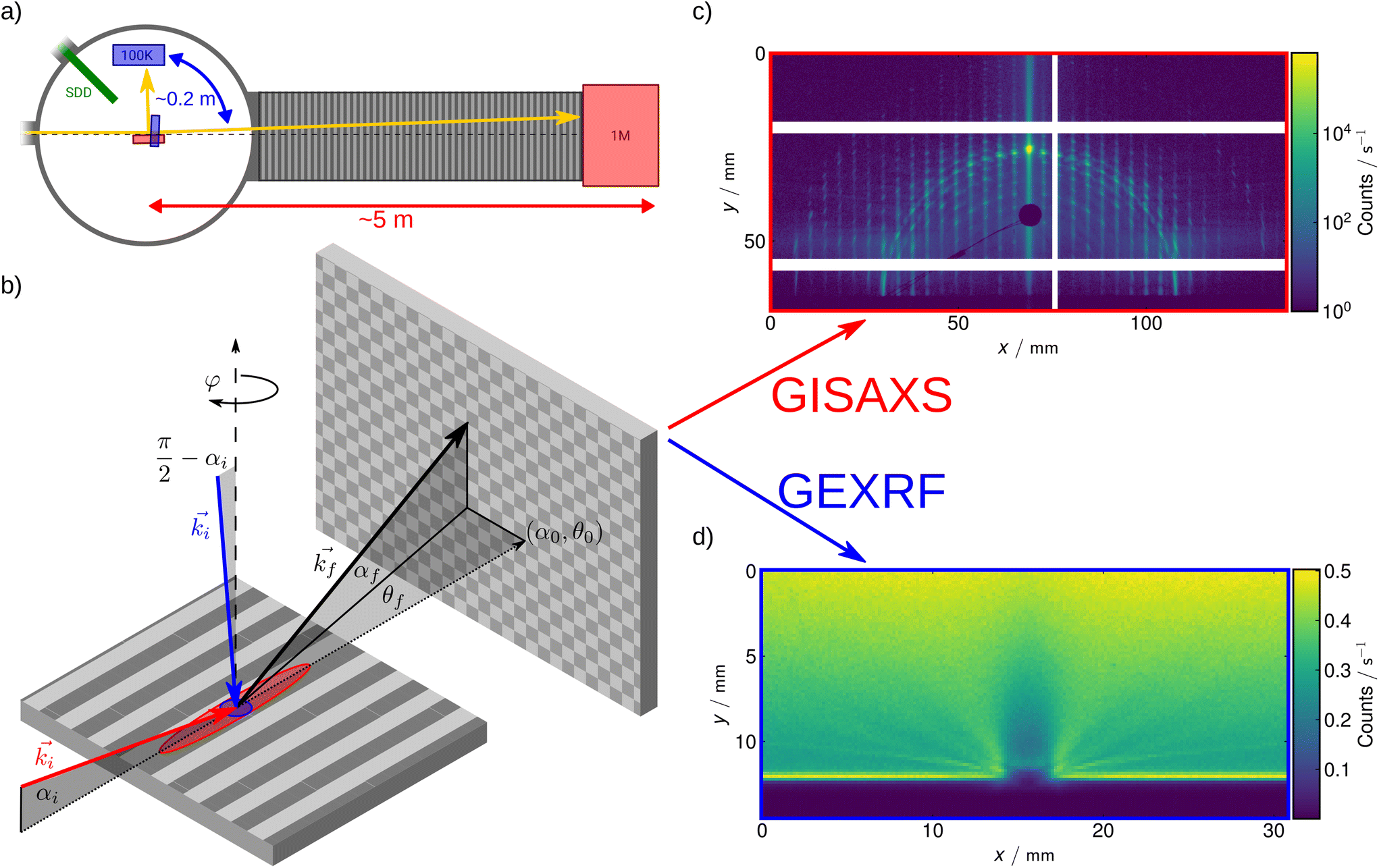 | ||
Fig. 1 (a) Side view of the sample chamber (reflectometer) with the position of the silicon drift detector (green), the rotatable in-vacuum PILATUS3 100K module used for the GEXRF experiment (blue), the PILATUS 1M detector of the GISAXS experiment (red) and their sample-detector distances. The corresponding sample position is also shown. (b) The scattering setup. An incoming wave vector  impinges on the sample under an incidence angle αi, which is small (<0.6°) for GISAXS (red) and close to 90° for GEXRF (blue). Scattered radiation (GISAXS) and fluorescence radiation (GEXRF) hit the detector at a position (αf, θf). Raw detector images taken as part of (c) the GISAXS and (d) the GEXRF experiment. impinges on the sample under an incidence angle αi, which is small (<0.6°) for GISAXS (red) and close to 90° for GEXRF (blue). Scattered radiation (GISAXS) and fluorescence radiation (GEXRF) hit the detector at a position (αf, θf). Raw detector images taken as part of (c) the GISAXS and (d) the GEXRF experiment. | ||
The following subsections describe the GISAXS and the GEXRF setups, the samples, as well as the computational model and corresponding virtual experiments. A sketch of the angle convention for GISAXS and GEXRF can be found in Fig. 1b.
2.1. GISAXS
The beam profile is defined with a pinhole of 520 μm diameter. A further pinhole of 1 mm diameter and positioned in front of the sample is used to shield parasitic scattering. At the sample position the beam size is about 0.1 mm × 0.4 mm (vertical × horizontal). Due to the grazing incidence angles this results in an elongated footprint on the specimen.The sample is measured in the so-called conical mounting, i.e. with the grating lines parallel to the direction of the beam (Fig. 1b). The intersection of the grating in the reciprocal space with the Ewald sphere leads to diffraction orders (Fig. 1c). The energy of the incoming photon beam is 6 keV. Measurements are taken at different angles of incidence (not larger than 1.5°) and different rotation angles φ in order to map several parts of the reciprocal space and obtain more information about the structure. The GISAXS images are collected on the large PILATUS 1M detector. The first three diffraction orders are neglected in the evaluation because they overlap with the scattering from neighbouring structures on the sample due to the elongated footprint. Only the intensities of higher diffraction orders could be spatially separated and identified on the detector.
2.2. Scanning-free GEXRF
The GEXRF experiment utilizes the same setup, but the sample is oriented such that the synchrotron radiation beam impinges on the sample at an angle of about 90°. This results in a smaller illumination area on the sample, with the beam footprint measuring roughly 0.1 mm × 0.4 mm (height × width). This is approximately two orders of magnitude smaller than the footprint in the GISAXS experiment, which is about 10 mm long. The primary fluorescence radiation is emitted isotropically over the entire solid angle of 4π, but at interfaces this radiation can be reflected and diffracted leading to interference effects.In order to detect the GEXRF interference pattern the movable PILATUS3 100K module is positioned in the region of the sample horizon. A raw detector image of such a GEXRF measurement can be seen in Fig. 1d.
Since the incoming photon flux, exposure time and quantum efficiency22 of the PILATUS3 100K detector are known, the intensities can be transformed into a quotient of emitted fluorescence flux per incoming photon flux (ϕ/ϕ0) as a function of the emission angles after correcting for the varying solid angle of the pixels due to the close distance between the detector and the sample. A representation of this geometry is shown in Fig. 1b.
Fig. 2a depicts an incident energy scan of a titanium dioxide grating over the titanium absorption edge measured with the SDD and PILATUS3 100k detector simultaneously. This validates that the photons detected by the area detector originate from X-ray fluorescence. Details on the use of area detectors for near edge X-ray absorption experiments can be found elsewhere.25,26 The region of interest (ROI) of the SDD is set to the titanium Kα energy. For the area pixel detector, a region without a diffraction ring (i.e., elastic scattering) is used. The PILATUS3 100K is not energy dispersive like the SDD, but it does have a detection threshold that is normally at 50% of the incoming photon energy.22 Therefore, the signal is always a superposition of all X-ray fluorescence signals present in the detectable energy range. In the GEXRF experiment used for the reconstruction and comparison with GISAXS, the same incoming photon energy of 6 keV is used.
 | ||
| Fig. 2 (a) Simultaneous near edge X-ray absorption fine structure (NEXAFS) measurement of a titanium dioxide grating at the Ti K edge with the SDD and the PILATUS3 100K detector. Both are normalized to the current of a monitor diode that measures the direct beam. (b) Fluorescence spectra of a titanium dioxide grating with additional chromium layer measured with the SDD for the four photon energies used in the GEXRF experiment. The (|) marks the photon energy of the incoming radiation, and the positions of the X-ray fluorescence Kα and Kβ lines of Ti and Cr are shown as vertical lines. | ||
To exploit the elemental sensitivity of GEXRF, use is made of different incident photon energies around the absorption edges of the K shell of the two main components of the sample structure, namely titanium and chromium. This is different from GEXRF methods that utilize an energy dispersive detection scheme.17 Only if the incident photon energy is above the absorption edge of the element will the related X-ray fluorescence of this element be emitted. Fig. 2b shows the energy range around the Ti and Cr characteristic fluorescence lines of a titanium dioxide grating with additional chromium layer measured with the SDD for four different incident photon energies. At E = 5.1 keV, which is above the titanium absorption edge, titanium Kα and Kβ fluorescence is emitted at 4512.2 eV and 4933.4 eV, respectively.27 In addition, at an energy of 6.1 keV, chromium fluorescence from the sample is observed with EKα = 5414.9 eV and EKβ = 5946.8 eV.27
2.3. Sample systems
For the experiments, lamellar titanium dioxide gratings with a period of 104.5 nm are investigated. These are produced as depicted in Fig. 3a employing an SADP technique. Since the gratings are used as deep ultraviolet (DUV) polarizers,28 they need to have a smaller period than the incoming DUV wavelength as well as a high aspect ratio.29 To produce the titania-polarizer, a stack of polymer, chromium, and e-beam resist layers is fabricated on a substrate of fused silica. The polymer and chromium layers are structured by e-beam lithography and successive ion beam etching. The resulting grid is the template grating of the DUV polarizer, so the height of the polymer is the main determinant of the height of the polarizer lines. The template grating of such a polarizer must have a pitch of 209 nm and a nominal height of 150 nm. The grid is then coated with the polarizer material (titanium dioxide) by atomic layer deposition.30 Ion beam etching is used to remove the remaining material in the valleys and on the top of the structure together with the chromium. The substrate serves as an etch-stop to ensure that overetching into the substrate does not exceed a few nanometres. In a later step, the polymer is removed by reactive ion etching with oxygen. Ideally, the obtained TiO2 polarizer will have a pitch of 104.5 nm, which is half the pitch of the template grating. Any artifact produced in the template grating is transferred to the polarizer. These deviations can lead to superstructures in the periodicity, which are often referred to as pitchwalk. A TEM cross section image of this sample A is shown in Fig. 3c. The structure is bent inward in pairs. This is caused by the relief of the internal layer stress when the template grating is removed. The deviation of such polarizer gratings from the ideal rectangular shape, including tilting and line edge roughness is discussed in detail elsewhere.28 | ||
| Fig. 3 (a) Self-aligned double patterning (SADP) process used for manufacturing the samples. (1 & 2) e-beam lithography and ion beam etching, the template grating is created, (3) polarizer material coated onto the template structure and (4) chrome and polymer removed by ion etching. Depending on the width of the template grating and the thickness of the polarizer material, different distances between the lines are obtained. The black rectangles show how this pitchwalk changes the position of the lines with respect to the red spacers, which are located at half the period of the template pitch. (b) Model used for the computation of the electric field. Shown are the main parameters that are optimized. (c) TEM cross section image of a witness sample A produced with a template pitch of 209 nm. | ||
An additional TiO2 grating, referred to as sample B, was produced with a chromium layer as a second element on top of the structure to simulate remaining residues. The reason for using chrome is that it resembles hard mask residue, which may be insufficiently removed in a real-world process. This sample system and the derived finite element method (FEM) model are depicted in Fig. 4.
 | ||
| Fig. 4 FEM model as taken from the TEM cross section of sample B. The colours in the image correspond to the different materials assigned to the mesh, namely fused silica substrate (red), TiO2 (green), Cr (orange) and vacuum (blue). The white bar is the scale of the TEM image. | ||
2.4. Modelling
The reconstruction of nanostructured surfaces using scattering intensities or angular-resolved fluorescence maps consists of an optimization problem based on a forward modelling of the experiment.7,31 A rigorous Maxwell solver is used to compute the electric field distribution in and around the periodic nanostructures. It allows the calculation of arbitrary shapes and through post-processing the relevant signals for scattering and fluorescence can be obtained simultaneously. The software used in this study is JCMsuite.32The sample (Fig. 3c) consists of a periodic pattern with mirror symmetry. Along the lines no variation is considered, so it is possible to reduce the 3D problem and calculate just the 2D plane perpendicular to the grating line. The computational domain is shown in Fig. 3b. It has periodic boundary conditions in the lateral direction and transparent boundaries at the top and at the bottom. The maximum length constraint of the finite elements was set to 5 nm and the polynomial degree to 4 to ensure sufficient numerical precision.
The model for sample A, which was used in the characterization of the structure by both the GISAXS and the GEXRF experiment, has a boxlike shape with parameters for width, height, pitchwalk and etch depth. In addition two variables are added to tilt the upper segment of the box symmetrically (Fig. 3b) in an attempt to reproduce the collapse of the structure, which is a result of the SADP manufacturing process.
The calculated complex electric field distribution of the near field is further processed for the different methods. In GISAXS, the post-processing consists of a Fourier transform that allows the estimation of the diffracted intensities. These are very sensitive to any variation of the line, i.e. line edge roughness,8,33–35 so such variation must be considered in any reconstruction process. To account for line edge roughness, a Debye–Waller factor is usually included in the computation of the diffracted intensities in GISAXS.18
As multiple modalities may exist, the fitting of scattering models to measurement data requires optimization methods that search globally for the minimum.18 For the GISAXS data reconstruction the built-in Bayesian optimizer of JCMsuite was used. It has been shown previously that this method reaches a global minimum with fewer iterations than metaheuristic methods and is more resilient to being trapped in a local minimum.36 In order to further speed up the convergence of the Bayesian optimizer, the scale factor of each of the measurements was fitted by a nested optimization using a local optimizer of SciPy.37
For the GEXRF reconstruction only subsets of the measured data at selected values of θf∈(0°, 0.7°, 1.5°), which is the in-plane angular deflection from the centre of the GEXRF feature (Fig. 1b), are fitted to the parameterized model. For these angle sets, the standing wave field in proximity of the structure is determined. The field inside the TiO2 and Cr is extracted, and the square of the absolute value, which is the field intensity, is compared to the experimental data from the area detector because it is proportional to the emitted fluorescence of the material.17,38 The principle of microscopic reversibility allows using GEXRF calculation tools developed for GIXRF by setting the photon energy of interest to that of the fluorescence photons instead of that of the incident photons.13 The emitted fluorescence photon is considered an incoming photon with the fluorescence energy of the titanium Kα line and the direction of the area detector pixel. This corresponds to an inversion of the problem, which is possible due to the temporal invariance of Maxwell's equations. A linear function is used as a background that is the same for all chosen θ and is fitted globally. This is a valid approximation for a bulk fluorescence signal with surface roughness.39 For the GEXRF optimization, the model was fitted by minimizing χ2 using a differential evolution (DE) algorithm as implemented in SciPy.37,40 In contrast to the machine learning algorithms mentioned above, DE in our case allows us to sample significantly larger parameter ranges, which is a considerable advantage for measurement methods that have not yet been standardized as it allows us to better detect unknown influences in the virtual experiment.
To demonstrate the element sensitivity of the GEXRF method we measure sample B with an additional chromium layer on top of the titanium structure. From a TEM cross section image a finite element model of this structure is extracted and the different material properties are assigned to the corresponding parts of the mesh (Fig. 4). This model is applied in forward calculations and compared to the experimental data.
In all GEXRF calculations, the bulk densities are used as material properties to reduce the computational effort, but in principle they could also be optimisation parameters. This should improve the agreement of calculation and measurement even more.
3. Results
The applicability of GEXRF for a quantitative structure reconstruction is verified by using sample A, which only consists of a TiO2 nanostructured surface. This structure is measured using the GEXRF method and simultaneously with GISAXS. For both measurements a structure reconstruction is conducted using the same model. Table 1 contains the summary of the optimization results of the main model parameters for both methods. The GEXRF result for the critical dimensions, namely width and height, is larger than the values obtained by GISAXS, indicating an increased amount of titanium. Moreover, the collapse of the structural model is much more pronounced in the fluorescence results. This is most likely the reason for the difference observed in the etch height. The discrepancy can be attributed to the different measurement regions and thus to the different mean sample structures investigated, as well as to the sensitivities of the methods used. Some of these aspects are highlighted below.| Width/nm | Height/nm | Pitchwalk/nm | Etch/nm | Tilt height/nm | Tilt angle/° | Roughness/nm | |
|---|---|---|---|---|---|---|---|
| Nominal | 40.0 | 150.0 | — | — | — | — | — |
| GISAXS | 42.1 | 139.7 | 7.3 | 3.4 | 13.3 | 35.9 | 3.1 |
| GEXRF | 55.6 | 147.6 | 12.3 | 16.0 | 41.2 | 50.0 | — |
For the reconstruction of nanostructures in GISAXS, the intensity of the diffraction orders is normally used. Samples produced by multiple patterning with pitchwalk have been previously characterized using GISAXS41 and SAXS.42 The same parameter reconstruction procedure used in these studies was also applied in the current investigation. The scattering pattern of this structure shows diffraction orders caused by the template pitch, which is twice the polarizer pitch. In addition, the scattering pattern also shows scattered intensities from surrounding areas. A pitch of 222 nm from a neighbouring grating is identified in the scattering pattern. This causes the superposition of the diffracted intensities at low orders of diffraction, whereas at high diffraction orders those two signals are well separated. For this reason, the low diffraction orders, which are usually more intense, are not considered in the reconstruction.
A representative comparison between the measured data and the fit is shown in Fig. 5. The leading contribution to the uncertainties in GISAXS is the computational error, which accounts for the assumptions and approximations performed to speed up the computation. The comparison clearly shows that even the two-dimensional GISAXS simulations reach their nanometrological limits due to the complexity of this sample. An almost perfect fit with sub-nanometre uncertainties in the reconstructed parameters, which can be expected with very simple lamellar grating reconstructions,7,18 cannot be achieved here. The SADP process probably leads to irregularities that can no longer be described with Debye–Waller damping approximations for the line edge roughness, which at 3.1 nm also appears to be quite high, but this value is also very close to the 3.6 nm extracted from SEM measurements on similar samples.43 Other lateral defects probably need to be included in the evaluation as well. For example, the dimensions of the structure are not discrete, but rather a distribution of sizes.
 | ||
| Fig. 5 Comparison between GISAXS measurement (data points) and fit (lines) for different diffraction orders (n) and for different angles of incidence (αi) on sample A. | ||
The measured GEXRF image of sample A is shown in Fig. 6a in comparison to the overall map calculated from the optimization result. The red vertical dashed lines indicate the slices that are used in the optimization process. The comparison of the GEXRF data with the fit for these slices is presented in Fig. 6b. The overall agreement of the calculated angular fluorescence with the experimental data is already quite good. All the features of the signal are also present in the calculation, but the experimental image looks more blurred/smooth. This is due to the relatively large pixel size of the detector and the close proximity to the sample, resulting in a very limited angular resolution. To account for this fact in the discrete angular calculations a Gaussian filter with σ = 0.5 is used in the post processing of the image. The signal close to the sample horizon is reproduced very well, whereas the smaller GEXRF features have some deviations in the angular position. The difference in intensity in some regions (e.g., the sample horizon) of the 2D image may be explained by the inhomogeneity and complex structure of the sample and the simplified model that extends with perfect periodicity in all lateral directions (see Fig. 3b and c). It does not, for example, contain any form of line edge roughness, which is quite high in this sample, as shown by the GISAXS results. Another cause for further blurring is the Ti Kβ emission, which contributes about 10% to the fluorescence signal and is present in the experimental data, but which is not considered in the calculation. The emission line is roughly 420 eV away from the Ti Kα line and therefore changes the angular fluorescence map. Since the experiment is performed with near normal incidence of the incoming photons, there is also a contribution of photons scattered from the bulk of the substrate, which results in a linear background for all θ.39 This is taken into account in the calculations by considering a linear background to the fluorescence signal calculated from the near field.
 | ||
| Fig. 6 (a) Experimental GEXRF Ti-K data for sample A (left) versus calculated map of the best-fit solution (right) for different emission angles θf and αf above the sample horizon. The vertical dashed lines denote the slices that are used in the optimization process. (b) Fit (red line) and experimental data points for the slices. In addition, the background (dashed line) and residuals (blue line) are shown. | ||
In principle, we are able to reproduce superposition of different fluorescence emissions. This is nicely demonstrated by the experiment on sample B, where, in addition to titanium, chromium is also present on the top and bottom of the structure (Fig. 4). The comparison of the measured GEXRF data and the forward simulation obtained from the TEM profile can be found in Fig. 7. For the experiment at an incident photon energy of Ei = 5.1 keV the map is calculated with the energy of the Ti Kα line, whereas the GEXRF data at Ei = 6.1 keV is reproduced by a superposition of the Ti Kα line and the Cr Kα line. The two very different fluorescence maps for both excitation photon energies agree well with the calculations. The size distribution and shape variation of the real sample structure is greater, as can be seen from the TEM image. This results in further blurring of the signal and additional attenuation near the sample horizon.
 | ||
| Fig. 7 Comparison between measured GEXRF data for sample B (left) and calculation (right) based on the TEM model. The incoming photon energies are 5.1 keV and 6.1 keV. For the calculation, energies of the titanium Kα and chromium Kα lines are used instead. | ||
4. Conclusion and outlook
In this work, we presented an initial comparison between the GEXRF measurement technique and classic GISAXS X-ray scatterometry for dimensional nanometrology. X-ray scattering techniques such as GISAXS are in principle ideal candidates to achieve sub-nanometre resolutions in the reconstruction of nanostructured surfaces but are severely limited by their large illumination spot on the sample under investigation.As shown here, grazing emission techniques such as GEXRF can circumvent this limitation because the area of interest is defined only by the size of the excitation beam.17 Measurements with both techniques are basically very straightforward thanks to the use of the scanning-free techniques enabled by modern flat hybrid pixel detectors. However, as the study illustrates, modern fabrication techniques for nanostructures such as SADP represent a challenge for both methods. Further challenges lie in the need for forward simulations of the reflected, scattered or emitted photons. The SADP method leads to a doubling of the domain to be calculated. However, this doubling in necessary simulation time can, as shown, be very effectively limited by applying advanced machine learning optimization methods. A larger effect on the quality of the simulations is the fact that the current models are limited to two dimensions, meaning that lateral inhomogeneities of the sample cannot be considered easily. However, a direct comparison should not ignore the fact that GISAXS and GEXRF examine different sample areas and thus a different mean sample structure in the case of lateral inhomogeneities. In addition, the effect of line edge roughness is not included in the model of GEXRF. From this point of view, the agreement between the two line shapes determined from the respective reconstruction is already very good for the present sample. In general, it should be possible to access the uncertainties for the reconstructed parameters in GEXRF using another optimisation algorithm (e.g. Bayesian optimiser). This has been demonstrated for GIXRF31 and a similar approach should work for GEXRF. An even better way to determine the uncertainties would be the complete mapping of the parameter space by a Markov chain Monte Carlo algorithm. Unfortunately, this technique requires a large number of function evaluations (usually over 500![[thin space (1/6-em)]](https://www.rsc.org/images/entities/char_2009.gif) 000). As a single calculation is currently still very time-consuming, this is not yet feasible.
000). As a single calculation is currently still very time-consuming, this is not yet feasible.
Sample B demonstrates quite impressively the potential of element-sensitive simulation, which can be used to investigate only certain relevant parts of the nanostructures. This is achieved by tuning the incoming photon energy above the corresponding absorption edges of the involved materials (Ti, Cr), in contrast to methods that use an energy-dispersive detector.17 The nanostructures are more complex than what can be described in terms of simple geometric shapes such as rectangles or trapezoids. A parametrization of such a line shape is also not trivial and would have to be oriented more to the process variations to be expected in production. But the high agreement of the forward simulation derived from a TEM image with the measured data for the different excitation energies is not only an example of the potential of GEXRF but also impressively demonstrates the flexibility of the finite element method. In summary, it can be concluded that GEXRF has a high potential to establish itself as a measurement method for dimensional and analytical nanometrology. The lack of resolution due to a small detector sample distance can be easily solved in future by optimized detection setups. The ever-increasing complexity in the production of nanostructured surfaces and the extension of the structures into the third dimension are an enormous challenge for the evaluation of any measurement technique, as the comparison with GISAXS has clearly shown.
Author contributions
Dieter Skroblin: formal analysis, investigation, writing – original draft, writing – review & editing. Analía Fernández Herrero: formal analysis, investigation, writing – original draft, writing – review & editing. Thomas Siefke: resources, writing – review & editing. Konstantin Nikolaev: conceptualization, investigation, writing – review & editing. Anna Andrle: investigation, writing – review & editing. Philipp Hönicke: conceptualization, investigation, writing – review & editing. Yves Kayser: conceptualization, investigation, writing – review & editing. Michael Krumrey: resources, writing – review & editing, project administration. Christian Gollwitzer: resources, writing – review & editing, supervision. Victor Soltwisch: conceptualization, formal analysis, investigation, writing – original draft, writing – review & editing, supervision.Conflicts of interest
There are no conflicts to declare.Acknowledgements
This project has received funding from the Electronic Component Systems for European Leadership Joint Undertaking under grant agreement no 826589 – MADEin4. This Joint Undertaking receives support from the European Union's Horizon 2020 Research and Innovation Programme and from the Netherlands, France, Belgium, Germany, the Czech Republic, Austria, Hungary, and Israel. This project has also received funding from the ECSEL Joint Undertaking (JU) under grant agreement no 875999 – IT2, as well as from the EMPIR programme 20IND04 ATMOC. The JU receives support from the European Union's Horizon 2020 Research and Innovation Programme and from the Netherlands, Belgium, Germany, France, Austria, Hungary, the United Kingdom, Romania, and Israel.References
- N. G. Orji, M. Badaroglu, B. M. Barnes, C. Beitia, B. D. Bunday, U. Celano, R. J. Kline, M. Neisser, Y. Obeng and A. E. Vladar, Nat. Electron., 2018, 1, 532–547 CrossRef PubMed.
- J. Villarrubia, A. Vladár, B. Ming, R. Kline, D. Sunday, J. Chawla and S. List, Ultramicroscopy, 2015, 154, 15–28 CrossRef CAS PubMed.
- R. Erni, M. D. Rossell, C. Kisielowski and U. Dahmen, Phys. Rev. Lett., 2009, 102, 096101 CrossRef PubMed.
- W. Häßler-Grohne, D. Hüser, K.-P. Johnsen, C. G. Frase and H. Bosse, Meas. Sci. Technol., 2011, 22, 094003 CrossRef.
- G. Dai, L. Xu and K. Hahm, Meas. Sci. Technol., 2020, 31, 074011 CrossRef CAS.
- B. Bunday, Proc. SPIE, 2016, 9778, 136–169 Search PubMed.
- V. Soltwisch, A. Fernández Herrero, M. Pflüger, A. Haase, J. Probst, C. Laubis, M. Krumrey and F. Scholze, J. Appl. Crystallogr., 2017, 50, 1524–1532 CrossRef CAS.
- H. S. Suh, X. Chen, P. A. Rincon-Delgadillo, Z. Jiang, J. Strzalka, J. Wang, W. Chen, R. Gronheid, J. J. d. Pablo, N. Ferrier, M. Doxastakis and P. F. Nealey, J. Appl. Crystallogr., 2016, 49, 823–834 CrossRef CAS.
- J. R. Levine, J. B. Cohen, Y. W. Chung and P. Georgopoulos, J. Appl. Crystallogr., 1989, 22, 528–532 CrossRef CAS.
- G. Renaud, R. Lazzari and F. Leroy, Surf. Sci. Rep., 2009, 64, 255–380 CrossRef CAS.
- M. Pflüger, V. Soltwisch, J. Probst, F. Scholze and M. Krumrey, IUCrJ, 2017, 4, 431–438 CrossRef PubMed.
- D. K. G. de Boer, A. J. G. Leenaers and W. W. van den Hoogenhof, X-Ray Spectrom., 1995, 24, 91–102 CrossRef CAS.
- R. S. Becker, J. A. Golovchenko and J. R. Patel, Phys. Rev. Lett., 1983, 50, 153–156 CrossRef CAS.
- Y. Kayser, J. Szlachetko, D. Banaś, W. Cao, J.-C. Dousse, J. Hoszowska, A. Kubala-Kukuś and M. Pajek, Spectrochim. Acta, Part B, 2014, 88, 136–149 CrossRef.
- Y. Kayser, P. Hönicke, D. Banaś, J.-C. Dousse, J. Hoszowska, P. Jagodziński, A. Kubala-Kukuś, S. H. Nowak and M. Pajek, J. Anal. At. Spectrom., 2015, 30, 1086–1099 RSC.
- V. Szwedowski-Rammert, J. Baumann, C. Schlesiger, U. Waldschläger, A. Gross, B. Kanngießer and I. Mantouvalou, J. Anal. At. Spectrom., 2019, 34, 922–929 RSC.
- P. Hönicke, Y. Kayser, K. V. Nikolaev, V. Soltwisch, J. E. Scheerder, C. Fleischmann, T. Siefke, A. Andrle, G. Gwalt, F. Siewert, J. Davis, M. Huth, A. Veloso, R. Loo, D. Skroblin, M. Steinert, A. Undisz, M. Rettenmayr and B. Beckhoff, Small, 2021, 2105776 Search PubMed.
- A. Fernández Herrero, M. Pflüger, J. Probst, F. Scholze and V. Soltwisch, Opt. Express, 2019, 27, 32490–32507 CrossRef PubMed.
- J. Baumann, Y. Kayser and B. Kanngießer, Phys. Status Solidi B, 2021, 258, 2000471 CrossRef CAS.
- Y. Kayser, J. Szlachetko and J. Sá, Rev. Sci. Instrum., 2013, 84, 123102 CrossRef CAS PubMed.
- J. Wernecke, C. Gollwitzer, P. Müller and M. Krumrey, J. Synchrotron Radiat., 2014, 21, 529–536 CrossRef CAS PubMed.
- D. Skroblin, A. Schavkan, M. Pflüger, N. Pilet, B. Lüthi and M. Krumrey, Rev. Sci. Instrum., 2020, 91, 023102 CrossRef CAS PubMed.
- M. Krumrey and G. Ulm, Nucl. Instrum. Methods Phys. Res., Sect. A, 2001, 467–468, 1175–1178 CrossRef CAS.
- D. Fuchs, M. Krumrey, P. Müller, F. Scholze and G. Ulm, Rev. Sci. Instrum., 1995, 66, 2248–2250 CrossRef CAS.
- K. Shinoda, S. Sato, S. Suzuki, T. Uruga, H. Tanida, H. Toyokawa, Y. Terada and Y. Takagaki, J. Surf. Anal., 2009, 15, 295–298 CrossRef CAS.
- Y. Kayser, J. Sá and J. Szlachetko, Anal. Chem., 2015, 87, 10815–10821 CrossRef CAS PubMed.
- W. Elam, B. Ravel and J. Sieber, Radiat. Phys. Chem., 2002, 63, 121–128 CrossRef CAS.
- T. Siefke and S. Kroker, in Polarization Control by Deep Ultra Violet Wire Grid Polarizers, Springer International Publishing, Cham, 2018, pp. 359–374 Search PubMed.
- T. Siefke, D. Lehr, T. Weber, D. Voigt, E.-B. Kley and A. Tünnermann, Opt. Lett., 2014, 39, 6434–6437 CrossRef CAS PubMed.
- T. Siefke, S. Kroker, K. Pfeiffer, O. Puffky, K. Dietrich, D. Franta, I. Ohlídal, A. Szeghalmi, E.-B. Kley and A. Tünnermann, Adv. Opt. Mater., 2016, 4, 1780–1786 CrossRef CAS.
- A. Andrle, P. Hönicke, G. Gwalt, P.-I. Schneider, Y. Kayser, F. Siewert and V. Soltwisch, Nanomaterials, 2021, 11, 1647 CrossRef CAS PubMed.
- J. Pomplun, S. Burger, L. Zschiedrich and F. Schmidt, Phys. Status Solidi B, 2007, 244, 3419–3434 CrossRef CAS.
- P. Mikulík and T. Baumbach, Phys. Rev. B: Condens. Matter Mater. Phys., 1999, 59, 7632–7643 CrossRef.
- A. Kato and F. Scholze, Appl. Opt., 2010, 49, 6102–6110 CrossRef.
- M.-A. Henn, S. Heidenreich, H. Gross, A. Rathsfeld, F. Scholze and M. Bär, Opt. Lett., 2012, 37, 5229–5231 CrossRef PubMed.
- P.-I. Schneider, X. Garcia Santiago, V. Soltwisch, M. Hammerschmidt, S. Burger and C. Rockstuhl, ACS Photonics, 2019, 6, 2726–2733 CrossRef CAS.
- P. Virtanen, R. Gommers, T. E. Oliphant, M. Haberland, T. Reddy, D. Cournapeau, E. Burovski, P. Peterson, W. Weckesser, J. Bright, S. J. van der Walt, M. Brett, J. Wilson, K. J. Millman, N. Mayorov, A. R. J. Nelson, E. Jones, R. Kern, E. Larson, C. J. Carey, İ. Polat, Y. Feng, E. W. Moore, J. VanderPlas, D. Laxalde, J. Perktold, R. Cimrman, I. Henriksen, E. A. Quintero, C. R. Harris, A. M. Archibald, A. H. Ribeiro, F. Pedregosa and P. van Mulbregt, SciPy 1.0 Contributors, Nat. Methods, 2020, 17, 261–272 CrossRef CAS PubMed.
- V. Soltwisch, P. Hönicke, Y. Kayser, J. Eilbracht, J. Probst, F. Scholze and B. Beckhoff, Nanoscale, 2018, 10, 6177–6185 RSC.
- R. Klockenkämper and A. von Bohlen, Total-Reflection X-Ray Fluorescence Analysis and Related Methods, John Wiley & Sons, Inc., Hoboken, New Jersey, 2015 Search PubMed.
- R. Storn, J. Glob. Optim., 1997, 11, 341–359 CrossRef.
- M. Pflüger, R. J. Kline, A. Fernández Herrero, M. Hammerschmidt, V. Soltwisch and M. Krumrey, J. Micro/Nanolithogr., MEMS, MOEMS, 2020, 19, 1 Search PubMed.
- D. F. Sunday, S. List, J. S. Chawla and R. J. Kline, J. Appl. Crystallogr., 2015, 48, 1355–1363 CrossRef CAS.
- T. Siefke, M. Heusinger, C. B. R. Hurtado, J. Dickmann, U. Zeitner, A. Tünnermann and S. Kroker, Opt. Express, 2018, 26, 19534–19547 CrossRef CAS PubMed.
| This journal is © The Royal Society of Chemistry 2022 |