
 Open Access Article
 This Open Access Article is licensed under a Creative Commons Attribution-Non Commercial 3.0 Unported Licence
Black or red phosphorus yields the same blue phosphorus film†
Alessandro
Sala
 *ac,
Maria
Caporali
b,
Manuel
Serrano-Ruiz
b,
Francesco
Armillotta
c,
Erik
Vesselli
ac,
Francesca
Genuzio
d,
Tevfik Onur
Menteş
d,
Andrea
Locatelli
d,
Giovanni
Comelli
ac,
Cristina
Africh
a and
Alberto
Verdini
*e
*ac,
Maria
Caporali
b,
Manuel
Serrano-Ruiz
b,
Francesco
Armillotta
c,
Erik
Vesselli
ac,
Francesca
Genuzio
d,
Tevfik Onur
Menteş
d,
Andrea
Locatelli
d,
Giovanni
Comelli
ac,
Cristina
Africh
a and
Alberto
Verdini
*e
aCNR-IOM Materials Foundry, S. S. 14 km 163.5, Trieste, I-34149, Italy. E-mail: sala@iom.cnr.it
bCNR-ICCOM Institute of Chemistry of Organometallic Compounds, Via Madonna del Piano 10, Sesto Fiorentino, I-50019, Italy
cPhysics Department, University of Trieste, via Valerio 2, Trieste, I-34127, Italy
dElettra-Sincrotrone Trieste S.C.p.A, S.S. 14 km 163.5 in AREA Science Park, Trieste, I-34149, Italy
eCNR-IOM Materials Foundry, c/o Physics and Geology Department, University of Perugia, via A. Pascoli 2, Perugia, I-06123, Italy. E-mail: verdini@iom.cnr.it
First published on 3rd October 2022
Abstract
After the discovery of graphene, many other 2D materials have been predicted theoretically and successfully prepared. In this context, single-sheet black phosphorus – phosphorene – is emerging as a viable contender in the field of (2D) semiconductors. Phosphorene offers high carrier mobility and an anisotropic structure that gives rise to a modulation of physical and chemical properties. This opens the way to many novel and fascinating applications related to field-effect transistors and optoelectronic devices. In previous studies, a single layer of blue phosphorene intermixed with Au atoms was grown using purified black phosphorus as a precursor. Starting from the observation that phosphorus vapor mainly consists of P clusters, in this work we aimed at obtaining blue phosphorus using much less expensive purified red phosphorus as an evaporant. By means of microscopy, spectroscopy and diffraction experiments, we show that black or red phosphorus deposition on Au(111) substrates yields the same blue phosphorus film.
Introduction
Blue phosphorus (BlueP) is a two-dimensional (2D) semiconducting material postulated as a stable allotrope of elemental phosphorus by Tomànek et al. in 2014.1 Similar to its well-known 2D allotrope, black phosphorus (BlackP), BlueP is predicted to exhibit a band gap that depends on the number of stacked layers and on the in-plane strain, a high transport velocity of holes, and weak interlayer interaction – a condition required for easy exfoliation.1 For this reason, several first-principles studies have investigated its potential in nanoelectronic devices,2,3 energy storage,4 gas sensors5 and superconductors.6 For instance, heterostructures of BlueP with other 2D materials, such as graphene or h-boron nitride, are highly promising as anode materials for batteries,7,8 while its van der Waals assemblies with (III–V) semiconductors, such as BSe, show potential as photocatalysts for water splitting.9 Recently, Molle et al. demonstrated that epitaxially grown BlueP can be encapsulated in between a thin gold film and an Al2O3 capping layer that protects BlueP from ambient oxidation, thus opening its application in the field of electronic devices rivaling silicene.10 These findings have fueled the search for a viable strategy for the synthesis of BlueP. So far, the most promising route is based on evaporating thermally decomposed BlackP and depositing it on selected, well-ordered single-crystal metal surfaces, as the total energy required to convert the atomic arrangement (armchair puckering) of BlackP into that of BlueP (zigzag) is relatively low.1 With this method, Chen et al. successfully grew on Au(111) a monolayer of what was initially proposed as pure BlueP,11 and then revised as a 2D compound of BlueP islands connected by Au atoms, as a sort of BlueP–Au network.12 Afterwards, several research groups focused their work on the characterization of the band and crystal structure of such films,13–17 on the growth process18,19 and on the adsorption behavior of environmental gas molecules.20,21 In addition, the same growth strategy was extended to other substrates, such as Pt(111),22 Te/Au(111),23 GaN(001)24 and Si-intercalated on Au(111).25One of the main remaining problems concerning this growth procedure is its scalability, which is a fundamental step once a large-scale application is being considered. In the present work, we explore the possibility of growing BlueP directly from the commercially available red allotrope (RedP), which would make the molecular beam epitaxy (MBE) process free from BlackP, the synthesis of which is energy- and time-consuming and, thus, expensive. Although it is expected that on evaporation under the same conditions BlackP and RedP should give the same cluster composition, and therefore the same film structure, few studies have been performed on the growth of BlackP and RedP under ultra-high vacuum conditions, providing little information about cluster composition. In order to rule out any difference in the film structure due to possibly different cluster compositions, we performed a series of measurements on the P films in an ultra-high vacuum using identical growth conditions for both RedP and BlackP.
By means of scanning tunneling microscopy (STM), low-energy electron microscopy (LEEM) and photoelectron emission microscopy (PEEM), we demonstrate that the deposition of RedP on Au(111) yields exactly the same BlueP–Au network film as the one obtained by starting from BlackP. This demonstrates that the cluster composition is the same and shows a fabrication route that could be extended to a wide range of suitable substrates to grow BlueP in a much easier and more cost affordable way.
Results and discussion
The Au(111) surface was cleaned following the standard procedure: Ar+ ion sputtering, thermal annealing at 600 °C and a subsequent check for contaminants by means of X-ray photoemission spectroscopy (XPS) and low-energy electron diffraction (LEED). Commercially available pure RedP (purity 99.999% – Sigma Aldrich) and synthesized BlackP were evaporated in separate sessions on the clean substrate maintained at about 250 °C from two Knudsen cells heated at 320 °C, as previously described.11 At this temperature, RedP sublimates in the form of P clusters, mainly P4 (see Fig. S1 in the ESI†), similar to BlackP evaporation under comparable conditions.11 The high-resolution STM image presented in Fig. 1a shows the as-prepared surface with atomic resolution: the RedP deposition yields a surface reconstruction with a supercell (in green) that contains six protruding atoms organized in two mirrored triangles, separated by three atoms on each side and four depressions at the vertices of the cell. The intensity profile extracted along the blue dashed line (Fig. 1b) displays the lateral size of the supercell (1.42 nm), which is compatible with a (5 × 5) periodicity of the Au(111) substrate (5 × 0.288 nm) and the interatomic distance of the protruding atoms (0.32 nm). Notably, the atomically resolved image is identical to the one found for the BlueP–Au network synthesized by evaporation of BlackP under similar conditions.11,12,14,16,26 In that case, it was found that the six protruding atoms correspond to the upper side of the two mirrored triangular islands of BlueP. The expected atomic arrangement of a single layer of free-standing BlueP is sketched in Fig. 1c: viewed from the top, the unit cell is identified by two vectors (in red). The side view reveals that the atoms are not coplanar, but are arranged in two distinct heights. The ideal length of the unit cell vectors, 3.3 Å, is very close to the measured interatomic distance of the protrusions. In addition, large-scale STM topography (Fig. S3 in the ESI†) demonstrates that the observed atomic arrangement is uniform over the Au(111) surface. Hence, the analysis of STM images indicates that the deposition of RedP on Au(111) yields the same layer of the BlueP–Au network as observed for the deposition of BlackP. In order to prove this hypothesis, in the following, we propose a full comparison of the structural and electronic properties of the BlueP–Au network film on Au(111) synthesized from both red and black phosphorus precursors. The atomic structure of the BlueP/Au(111) surface can be probed with great precision by spatial and dynamic analyses of diffraction patterns yielded by backscattered low-energy electrons. Fig. 2 displays a direct comparison of kinematic LEED patterns measured from the BlueP layer grown from RedP (left) and BlackP (right) deposition. Here, a (5 × 5) superstructure develops on the Au(111) (1 × 1) pattern (described by the reciprocal space vectors in blue) upon growth of BlueP. It is evident that the phosphorus layer obtained either from RedP or BlackP yields identical energy-dependent LEED patterns, showing that the two films have the same atomic geometry. Indeed, the energy-dependent intensity modulation of the single diffraction spots presented in Fig. S3† confirms this statement in major detail. The I(V) characteristics of backscattered electrons is strongly dependent on the relative position of the atoms placed in the first few layers. Furthermore, the spot intensity also depends on the shape of the repeating unit and on the form factor, which includes the effects of multiple scattering, electron attenuation and phase shifting.27 | ||
| Fig. 1 (a) Atomically resolved STM topographic image of the BlueP/Au(111) surface prepared through the deposition of RedP. The (5 × 5) unit cell of the P-induced superstructure is indicated with a green rhombus, in which two mirrored triangular protrusions of three atoms each are included. The red arrows indicate the relative positions of the protruding atoms.12 The depressions at the unit cell's vertices appear sometimes partially filled by extra atoms.12 Scale bar 1 nm, bias −0.5 V, tunneling current 1.0 nA. The intensity line profile extracted along the blue dashed arrow is depicted in (b), where the unit cell length and the distance between protruding atoms are highlighted in green and red, respectively. (c) Top and side view of the ball and stick model of a single BlueP layer. Solid/empty circles indicate the atoms at the top/bottom plane, respectively. The red arrows define its two-dimensional unit cell. | ||
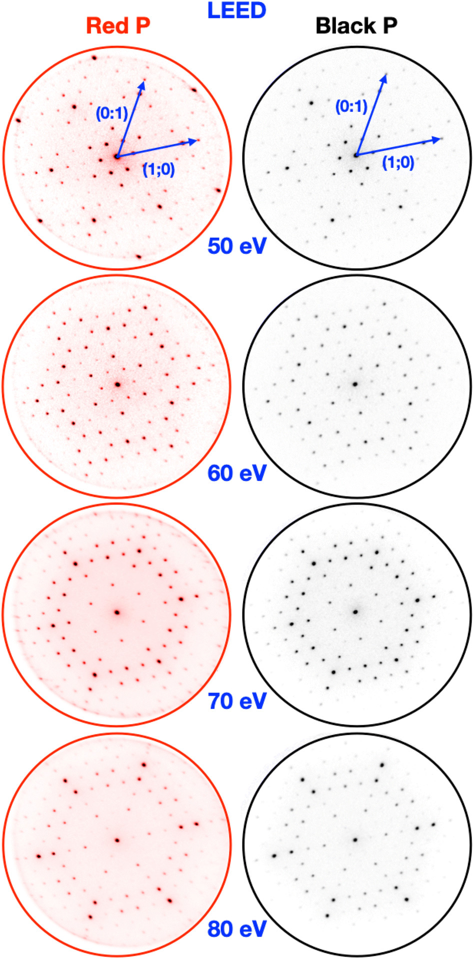 | ||
| Fig. 2 LEED patterns of BlueP/Au(111) grown from RedP (left, in red) and BlackP (right, in black) deposition are compared for four different kinetic energy values of the incident electrons. All LEED data were acquired at room temperature in the LEEM setup under UHV conditions. Blue vectors indicate the reciprocal unit cell vectors of Au(111). Spots at the border of the detector are distorted due to the spherical aberrations in the LEEM electron optics. | ||
The dynamic LEED analysis is capable of determining the position of atoms inside the unit cell within a fraction of an Å. Therefore, the fact that the I(V) curves compared as shown in Fig. S3† display identical peaks over an integrated range around 1820 eV, indicating that the two surfaces have the same structure. This is also confirmed by the very low value of the Pendry R-factor = 0.079 calculated over the entire I(V) dataset.
As the two atomic structures appear to be identical, they are expected to exhibit the same electronic structure. The electron band dispersion of the two films can be compared by probing the angular distribution of photoemitted electrons at a variable kinetic energy. Fig. 3a shows the angle-resolved photoelectron spectroscopy (ARPES) pattern mapped over the entire 2π angle at a corresponding electron binding energy (BE) of 1.2 eV, obtained by collecting the photoemitted electrons from a surface spot with diameter of 2 microns with 65 eV photons. The angular distributions of electrons emitted by BlueP/Au(111) grown from RedP or BlackP are again identical. In order to probe the band structure of both surfaces, we collected a stack of ARPES maps at different electron kinetic energies and extracted the momentum distribution curves (MDCs) along high-symmetry directions of the first Brillouin zone with a waterfall plot. The MDCs of the two samples, shown by excerpts along Γ–K and Γ–M axes, are displayed in Fig. 3b and c, and reveal identical features. Both waterfall images are in agreement with the experimental band structure reported in the literature.14–16 By comparing with the electron band dispersion of clean Au(111) measured under the same experimental conditions (Fig. S4 in the ESI†), one can identify the strong sp band of Au(111) at around 2.0 eV BE (highlighted with green arrows) and the absence of the Au(111) surface state around Γ at low BEs. Notably, the band structure induced by BlueP, indicated by blue arrows, is mainly present between 1.0 and 2.0 eV BEs,14,15 where it overlaps the f-band dispersion of Au(111) and its weak replicas produced by a (5 × 5) superstructure. Both RedP- and BlackP-originated surfaces exhibit an overall lack of the electron density of states for BEs lower than 1.0 eV, as already reported and interpreted as a sign of the semiconducting properties of BlueP.11
 | ||
| Fig. 3 Band structure comparison. (a) ARPES maps of BlueP/Au(111) grown from RedP (top) and BlackP (bottom) precursors, respectively. Photon energy is 65 eV and the binding energy is 1.2 eV. The high-symmetry points Γ, K and M of the Au(111) reciprocal unit cell are marked on the figure, while the relative Γ–K and Γ–M axes are drawn with red lines. The electron intensity distribution appears asymmetrical and slightly affected by chromatic aberrations. The momentum distribution curves, extracted from a stack of ARPES maps measured at variable electron kinetic energies, are displayed for both the samples along the Γ–K (b) and Γ–M (c) axes. The Fermi energy is indicated by a white dashed line at 0 eV. The x-axis origin is fixed at the Γ position. | ||
In addition to the comparison between different growth pathways, we monitored the thermal stability of BlueP/Au(111) grown from RedP by means of real-time LEEM imaging. In Fig. 4, we report the integrated intensity of the investigated area as a function of temperature while annealing at 0.6 K s−1. BlueP-covered areas appear dark in comparison with the uncovered Au(111) regions due to the different reflectivity at the particular electron kinetic energy chosen for imaging (16 eV). BlueP is very stable up to ∼625 K. Above this threshold, the dark areas start to lose contrast, which can be interpreted as the onset of film degradation at the nanometer scale, below the lateral resolution limit in LEEM. The fade-out process accelerates above 660 K, when all BlueP residing on large Au(111) terraces dissolves quickly. The most resilient parts, still present at 675 K, are those located near the substrate atomic steps, visible in LEEM as black lines across the surface. Above 680 K, no trace of BlueP is detected anymore; Au(111) appears clean but corrugated by the formation of atomic steps induced by the material bustle. Comparable LEEM observations of the thermal stability of BlueP grown from BlackP yielded identical results.
 | ||
| Fig. 4 Integrated intensity plot extracted from the LEEM images of Au(111) partially covered with BlueP, acquired in real time during annealing from 580 K to 690 K at a rate of 0.6 K s−1. LEEM images acquired at selected temperatures are displayed with a scale bar of 1.0 μm (white bar). At the selected electron kinetic energy (16 eV) the clean Au(111) surface appears bright and the BlueP adlayer appears dark. | ||
Conclusions
In summary, we demonstrated that BlueP films can be easily prepared by means of MBE using commercially available red phosphorus, instead of the much more expensive BlackP allotrope. This finding is supported by the perfect matching of STM topographic imaging, kinematic LEED patterns, LEED I(V) characteristics and electronic band structures extracted from ARPES patterns from the samples obtained with the two preparation methods. In other words, the morphological, structural and electronic properties of BlueP phases obtained from RedP and BlackP are shown to be identical. Because the red allotrope is widely available and produced on a large scale, this finding represents a huge advantage towards a more affordable production of BlueP-based model structures and devices.Experimental
Synthesis of black phosphorus
Crystals of black phosphorus were prepared according to a previously published procedure28 using commercial red phosphorus as the source of P, and Sn and SnI4 as mineralization additives. All the reagents were purchased from Sigma Aldrich and used as received.Scanning tunneling microscopy
STM experiments were carried out using a commercial Omicron Low-Temperature STM hosted at CNR-IOM Materials Foundry, Trieste, Italy, operating at 77 K under UHV conditions (base pressure < 8 × 10⁻¹¹ mbar) and coupled with a preparation chamber equipped with a sputter gun, a sample annealing stage and a Kentax TCE-BSC evaporator loaded with red phosphorus. STM topographic images were acquired in a constant-current mode and post-processed with drift correction and mild Gaussian smoothing Gwyddion software.Spectroscopic photo-emission and low energy electron microscopy
SPELEEM experiments were carried out at the Nanospectroscopy beamline of the Elettra synchrotron radiation facility, Trieste, Italy, with a soft X-ray beamline providing photons in a range of 10–1000 eV. The photon beam is focused at the sample (minimum spot size 25 × 2.5 μm2 along the horizontal and the vertical), onto which it impinges at an incidence angle of 16°. The beamline end-station is equipped with the SPELEEM (Elmitec GmbH), a hybrid electron microscope which uses low energy electrons (extracted from a LaB6 emitter) or X-rays as the probe.29,30 In the SPELEEM, the sample is the electron source (cathode). Backscattered or photoemitted electrons are accelerated by a 15 kV potential into the imaging column through the objective lens; the e-beam is then magnified by a system of electrostatic and magnetic lenses, filtered in energy and conveyed onto a 2D detector consisting of an MCP, a phosphorus screen and CCD (Retiga R6). The SPELEEM can perform multiple techniques such as real space imaging microscopy (LEEM/PEEM), micro-spot reciprocal space imaging (μ-LEED/μ-ARPES) and micro-spot spectroscopy (μ-XPS). In the imaging mode, the spatial resolution is below 10 nm. In our experiments, μ-LEED and μ-ARPES data were collected from a circular area of diameter 500 nm and 2000 nm, respectively, selected by inserting a field limiting aperture in the optical path of the e-beam. LEEM/LEED/ARPES data were acquired with an energy resolution of 0.33 eV. The LEEM images were obtained in the bright-field mode, i.e. by using the (0,0) elastically backscattered beam. The main chamber, working under UHV conditions (base pressure < 7 × 10⁻¹¹ mbar), was equipped with a Kentax TCE-BSC evaporator loaded with red phosphorus and black phosphorus, and was connected to a preparation chamber with standard sputtering/annealing stages.Author contributions
Alessandro Sala: methodology, investigation, data curation, visualization, and writing – original draft. Maria Caporali: resources, writing – review and editing. Manuel Serrano Ruiz: resources, writing – review and editing. Francesco Armillotta: investigation, writing – review and editing. Erik Vesselli: supervision, funding acquisition, writing – review and editing. Francesca Genuzio: investigation, writing – review and editing. Tevfik Onur Menteş: investigation, writing – review and editing. Andrea Locatelli: investigation, supervision, writing – review and editing. Giovanni Comelli: supervision, funding acquisition, writing – review and editing. Cristina Africh: supervision, funding acquisition, writing – review and editing. Alberto Verdini: conceptualization, methodology, investigation, writing – original draft, funding acquisition, project administration, and supervision.Conflicts of interest
There are no conflicts to declare.Acknowledgements
A. S., M. C., M. S. R., E. V. and A. V. acknowledge funding from the project “FERMAT – Fast ElectRon dynamics in novel hybrid organic-2D MATerials” funded by the MUR Progetti di ricerca di Rilevante Interesse Nazionale (PRIN) Bando 2017 – grant 2017KFY7XF.References
- Z. Zhu and D. Tománek, Phys. Rev. Lett., 2014, 112, 176802 CrossRef PubMed.
- M. Peruzzini, R. Bini, M. Bolognesi, M. Caporali, M. Ceppatelli, F. Cicogna, S. Coiai, S. Heun, A. Ienco, I. I. Benito, A. Kumar, G. Manca, E. Passaglia, D. Scelta, M. Serrano-Ruiz, F. Telesio, S. Toffanin and M. Vanni, Eur. J. Inorg. Chem., 2019, 1476–1494 CrossRef CAS PubMed.
- J. Li, X. Sun, C. Xu, X. Zhang, Y. Pan, M. Ye, Z. Song, R. Quhe, Y. Wang, H. Zhang, Y. Guo, J. Yang, F. Pan and J. Lu, Nano Res., 2018, 11, 1834–1849 CrossRef CAS.
- S. Mukherjee, L. Kavalsky and C. V. Singh, ACS Appl. Mater. Interfaces, 2018, 10, 8630–8639 CrossRef CAS PubMed.
- F. Safari, M. Moradinasab, M. Fathipour and H. Kosina, Appl. Surf. Sci., 2019, 464, 153–161 CrossRef CAS.
- J.-J. Zhang and S. Dong, 2D Mater., 2016, 3, 035006 CrossRef.
- Y. Li, W. Wu and F. Ma, J. Mater. Chem. A, 2019, 7, 611–620 RSC.
- J. Bao, L. Zhu, H. Wang, S. Han, Y. Jin, G. Zhao, Y. Zhu, X. Guo, J. Hou, H. Yin and J. Tian, J. Phys. Chem. C, 2018, 122, 23329–23335 CrossRef CAS.
- B.-J. Wang, X.-H. Li, R. Zhao, X.-L. Cai, W.-Y. Yu, W.-B. Li, Z.-S. Liu, L.-W. Zhang and S.-H. Ke, J. Mater. Chem. A, 2018, 6, 8923–8929 RSC.
- C. Grazianetti, G. Faraone, C. Martella, E. Bonera and A. Molle, Nanoscale, 2019, 11, 18232–18237 RSC.
- J. L. Zhang, S. Zhao, C. Han, Z. Wang, S. Zhong, S. Sun, R. Guo, X. Zhou, C. D. Gu, K. Di Yuan, Z. Li and W. Chen, Nano Lett., 2016, 16, 4903–4908 CrossRef CAS PubMed.
- S. Zhao, J. L. Zhang, W. Chen and Z. Li, J. Phys. Chem. C, 2020, 124, 2024–2029 CrossRef CAS.
- R. Swaroop, P. K. Ahluwalia, K. Tankeshwar and A. Kumar, RSC Adv., 2017, 7, 2992–3002 RSC.
- J. Zhuang, C. Liu, Q. Gao, Y. Liu, H. Feng, X. Xu, J. Wang, J. Zhao, S. X. Dou, Z. Hu and Y. Du, ACS Nano, 2018, 12, 5059–5065 CrossRef CAS PubMed.
- E. Golias, M. Krivenkov, A. Varykhalov, J. Sánchez-Barriga and O. Rader, Nano Lett., 2018, 18, 6672–6678 CrossRef CAS.
- W. Zhang, H. Enriquez, Y. Tong, A. Bendounan, A. Kara, A. P. Seitsonen, A. J. Mayne, G. Dujardin and H. Oughaddou, Small, 2018, 14, 1804066 CrossRef PubMed.
- H. Tian, J.-Q. Zhang, W. Ho, J.-P. Xu, B. Xia, Y. Xia, J. Fan, H. Xu, M. Xie and S. Y. Tong, Matter, 2020, 2, 111–118 CrossRef.
- J.-P. Xu, J.-Q. Zhang, H. Tian, H. Xu, W. Ho and M. Xie, Phys. Rev. Mater., 2017, 1, 061002 CrossRef.
- N. Han, N. Gao and J. Zhao, J. Phys. Chem. C, 2017, 121, 17893–17899 CrossRef CAS.
- N. Liu and S. Zhou, Nanotechnology, 2017, 28, 175708 CrossRef PubMed.
- J. L. Zhang, S. Zhao, M. Telychko, S. Sun, X. Lian, J. Su, A. Tadich, D. Qi, J. Zhuang, Y. Zheng, Z. Ma, C. Gu, Z. Hu, Y. Du, J. Lu, Z. Li and W. Chen, Nano Lett., 2019, 19, 5340–5346 CrossRef CAS PubMed.
- O. Heikkinen, H. Pinto, G. Sinha, S. K. Hämäläinen, J. Sainio, S. Öberg, P. R. Briddon, A. S. Foster and J. Lahtinen, J. Phys. Chem. C, 2015, 119, 12291–12297 CrossRef CAS.
- C. Gu, S. Zhao, J. L. Zhang, S. Sun, K. Yuan, Z. Hu, C. Han, Z. Ma, L. Wang, F. Huo, W. Huang, Z. Li and W. Chen, ACS Nano, 2017, 11, 4943–4949 CrossRef CAS.
- J. Zeng, P. Cui and Z. Zhang, Phys. Rev. Lett., 2017, 118, 046101 CrossRef.
- J. L. Zhang, S. Zhao, S. Sun, H. Ding, J. Hu, Y. Li, Q. Xu, X. Yu, M. Telychko, J. Su, C. Gu, Y. Zheng, X. Lian, Z. Ma, R. Guo, J. Lu, Z. Sun, J. Zhu, Z. Li and W. Chen, ACS Nano, 2020, 14, 3687–3695 CrossRef CAS PubMed.
- W. Zhang, H. Enriquez, A. J. Mayne, A. Bendounan, A. P. Seitsonen and G. Dujardin, Mater. Today: Proc., 2021, 39, 1153–1156 CAS.
- M. A. Van Hove, W. H. Weinberg and C.-M. Chan, Low-Energy Electron Diffraction, Springer Berlin Heidelberg, Berlin, Heidelberg, 1986, vol. 6 Search PubMed.
- M. Köpf, N. Eckstein, D. Pfister, C. Grotz, I. Krüger, M. Greiwe, T. Hansen, H. Kohlmann and T. Nilges, J. Cryst. Growth, 2014, 405, 6–10 CrossRef.
- A. Locatelli, L. Aballe, T. O. Menteş, M. Kiskinova and E. Bauer, Surf. Interface Anal., 2006, 38, 1554–1557 CrossRef CAS.
- T. O. O. Menteş, G. Zamborlini, A. Sala and A. Locatelli, Beilstein J. Nanotechnol., 2014, 5, 1873–1886 CrossRef PubMed.
Footnote |
| † Electronic supplementary information (ESI) available: Residual gas analyzer spectrum of the P clusters during evaporation of red phosphorus; angle-resolved photoemission spectroscopy patterns and electron band dispersion spectra of clean Au(111) surfaces. See DOI: https://doi.org/10.1039/d2nr02657k |
| This journal is © The Royal Society of Chemistry 2022 |