
 Open Access Article
 This Open Access Article is licensed under a Creative Commons Attribution-Non Commercial 3.0 Unported Licence
Enhanced excitonic features in an anisotropic ReS2/WSe2 heterostructure†
Arslan
Usman
 *af,
M.
Adel Aly
ab,
Hilary
Masenda
ac,
Joshua J. P.
Thompson
a,
Surani M.
Gunasekera
d,
Marcin
Mucha-Kruczyński
de,
Samuel
Brem
a,
Ermin
Malic
a and
Martin
Koch
a
*af,
M.
Adel Aly
ab,
Hilary
Masenda
ac,
Joshua J. P.
Thompson
a,
Surani M.
Gunasekera
d,
Marcin
Mucha-Kruczyński
de,
Samuel
Brem
a,
Ermin
Malic
a and
Martin
Koch
a
aDepartment of Physics and Materials Sciences Centre, Philipps-Universität Marburg, Marburg 35032, Germany. E-mail: arslan.usman@physik.uni-marburg.de
bDepartment of Physics, Faculty of Science, Ain Shams University, Cairo 11566, Egypt
cSchool of Physics, University of the Witwatersrand, 2050 Johannesburg, South Africa
dDepartment of Physics, University of Bath, Claverton Down, Bath BA2 7AY, UK
eCentre for Nanoscience and Nanotechnology, University of Bath, Claverton Down, Bath BA2 7AY, UK
fDepartment of Physics, COMSATS University Islamabad-Lahore-Campus, Pakistan
First published on 15th July 2022
Abstract
Two-dimensional (2D) semiconductors have opened new horizons for future optoelectronic applications through efficient light–matter and many-body interactions at quantum level. Anisotropic 2D materials like rhenium disulphide (ReS2) present a new class of materials with polarized excitonic resonances. Here, we demonstrate a WSe2/ReS2 heterostructure which exhibits a significant photoluminescence quenching at room temperature as well as at low temperatures. This indicates an efficient charge transfer due to the electron–hole exchange interaction. The band alignment of two materials suggests that electrons optically injected into WSe2 are transferred to ReS2. Polarization resolved luminescence measurements reveal two additional polarization-sensitive exciton peaks in ReS2 in addition to the two conventional exciton resonances X1 and X2. Furthermore, for ReS2 we observe two charged excitons (trions) with binding energies of 18 meV and 15 meV, respectively. The bi-excitons of WSe2 become polarization sensitive and inherit polarizing properties from the underlying ReS2 layers, which act as patterned substrates for top layer. Overall, our findings provide a better understanding of optical signatures in 2D anisotropic materials.
1. Introduction
Two-dimensional (2D) materials have gained immense research interest since the inception of graphene.1 The 2D family consists of a wide variety of layered materials which include metals, insulators, and semiconductors. The layered semiconductors hold strong excitonic features2–6 that can be tuned by external means by probing the physics of spin and valley polarization. Among all layered semiconductors, transition metal dichalcogenides (TMDs) exhibit exceptional optical, electrical, and topological properties when scaled down to monolayers. Most monolayers possess a direct bandgap in contrast to their bulk crystals. These ultrathin layers are promising materials for flexible, transparent, and robust electronic and optoelectronic devices such as photodetectors,7,8 solar cells9,10 and polarization sensitive switches.11 Large exciton binding energies (>100 meV)12 enabling excitons to overcome thermal dissociation at room-temperature are a consequence of enhanced quantum confinement and reduced dielectric screening.13 Another field of research that is emerging rapidly in the last few years is the formation of heterostructures14–18 by stacking monolayers of two different TMDs. These structures possess an atomically sharp and nearly defect-free interface.15 The stack represents a hybrid material arranged in a desired sequence.19,20 In such heterostructures interlayer excitons are formed because of the band alignment and an efficient charge transfer across the heterostructure interface.21,22 Such charge transfer excitons have characteristic features like long lifetimes and spin-valley polarization.23 Thus, the domain of two-dimensional materials and van der Waals heterostructures opens new avenues leading to a fast-growing research area in semiconductor technology. Typically, monolayers absorb about 10% of the incoming radiation in the visible range.The absorption gradually increases with an increasing number of layers and easily reaches ∼30% for thicker flakes. Following this concept, heterostructures with more than two monolayers show a considerable photon absorption. Consequently, the increased concentration of photo generated charge carriers leads to enhanced quantum efficiency that is crucial for photovoltaic and optoelectronic applications.
Rhenium disulphide (ReS2) is an anisotropic layered material from the VII-B group which has a layer independent bandgap due to its weak interlayer coupling and low crystal symmetry. It has a distorted 1T structure with Re–Re metallic atoms in a zig-zag chain-like geometry which is maintained via covalent bonds. This lack of ordering is the overriding reason for low interlayer coupling of ReS2.24 Importantly, with respect to its b-axis (metallic atomic chains) it shows a polarization sensitive optical excitation and emission. The fabrication of ReS2 based heterostructure and its integration in optoelectronic applications25–27 has not yet been explored extensively.
Here, we study the photoluminescence from a 2D layered heterostructure composed of a few-layers (FL) of rhenium disulphide covered with a monolayer of WSe2. The low-temperature luminescence spectrum shows numerous excitonic peaks with a distinct polarization dependence which includes charged trions and polarized bi-excitons that have not been reported yet. We have also investigated the exciton polarizability using polarization resolved PL. From the pronounced luminescence we conclude on an efficient charge transfer due to the distinct type II band alignment.28 The efficient charge transfer between ReS2 and WSe2 could be a promising basis for the application of such heterostructures in optoelectronic devices.
2. Methods and characterizations
A monolayer (ML) of WSe2 and a few layer (FL) flake of ReS2 were exfoliated from bulk crystals (2D Semiconductors, Inc.) on polydimethylsiloxane (PDMS) gel. A flake (few layers) of hexagonal boron nitride (hBN) was transferred using the standard viscoelastic stamping technique onto a 300 nm SiO2/Si substrate. The FL-ReS2 flake was then transferred on top of the hBN which acts as substrate. Secondly, a glass slide containing a monolayer of WSe2 on PDMS is well aligned and transferred on top of the ReS2 flake ensuring a good overlay for the heterostructure. The optical micrograph of the heterostructure is illustrated in Fig. 1(a), while panel (b) illustrates a schematic of the prepared heterostructure. The entire transfer process is done under a microscope using a manual controlled xyzθ stage with a 20× objective. During the transfer process before moving to the next step, each material on PDMS gel was characterized using Raman and photoluminescence (PL) spectroscopy. The heterostructure is also confirmed using atomic force microscopy, Fig. S2 (ESI).† Raman and PL spectra from each individual monolayer as well as from the overlap region confirms the proper material stacking and consequently reveals good interface quality. The crystallographic orientation was estimated by identifying the b-axis, as ReS2 is most likely to be cleaved along that direction (ESI, Fig. S2†).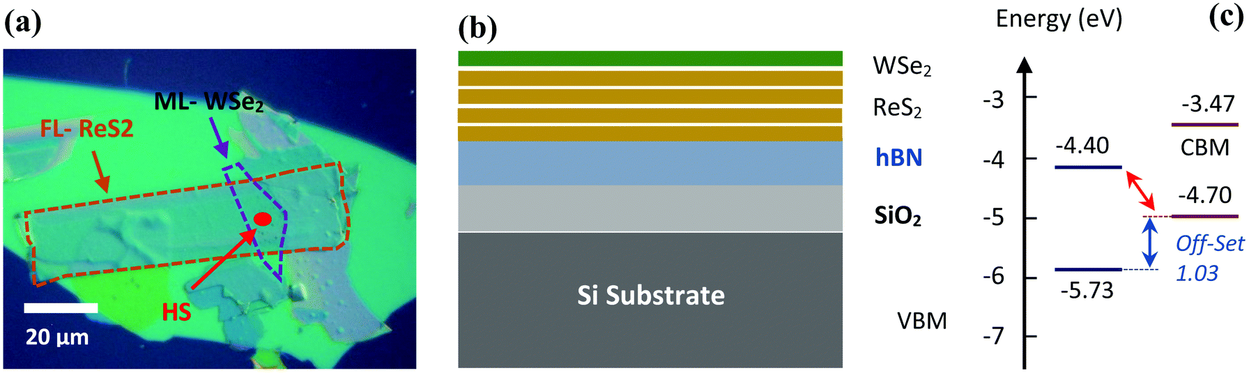 | ||
| Fig. 1 WSe2/ReS2 vertical heterostructure, (a). Optical micrograph with individual and overlay regions, (b). Schematic of vertical heterostructure, (c). Energy level diagram. | ||
3. Results and discussion
3.1 Photoluminescence
In this work, a steady state μ-PL setup is used to obtain the spectra of the two individual materials as well as their heterostructure. In the setup, which comprises a 40× objective, the sample is excited with a CW laser (λ = 532 nm). The emission signal is collected by the same objective and is analyzed by monochromator with a liquid nitrogen-cooled CCD detector (Princeton Instruments). The obtained spectra are shown in Fig. 2. WSe2 is a direct gap semiconductor at monolayer thickness with an emission peak at 1.64 eV as shown in Fig. 2(a), whereas few-layer ReS2 has a direct bandgap at 1.55 eV. The orange curve in the PL spectrum has one dominant peak at 1.64 eV, which we attribute to the neutral exciton (X°) of WSe2. In addition to that, the peak has a tail on the low energy side which suggests the presence of a weak additional peak red-shifted by ∼30 meV which originates from the negatively charged exciton (X−). This peak has already been observed for WSe2 in previous studies.29–32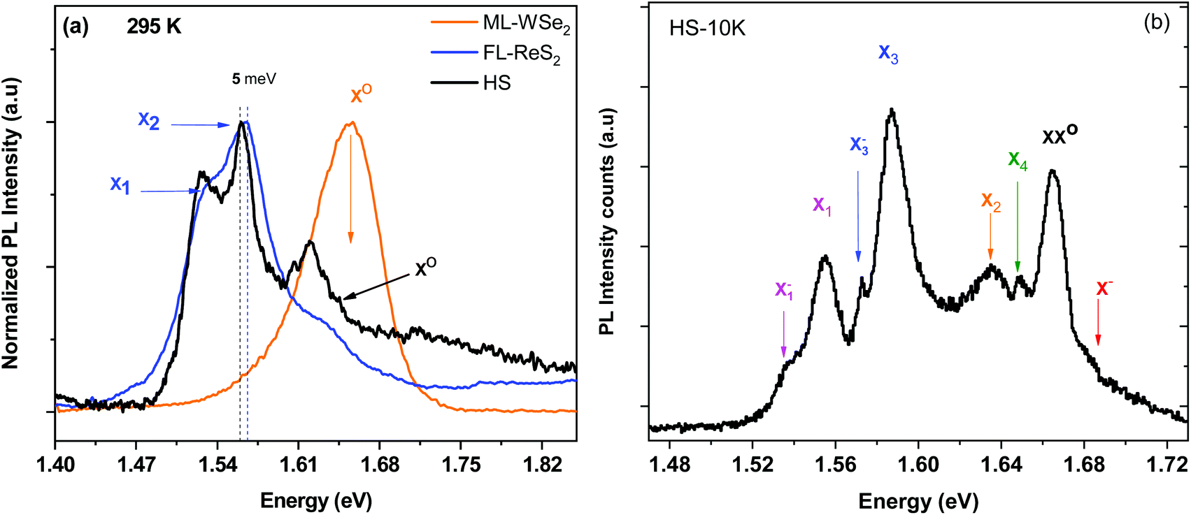 | ||
| Fig. 2 Photoluminescence spectra of monolayer WSe2, FL-ReS2 & their heterostructure at (a). 295 K (b). 10 K. | ||
The blue curve represents the emission from few-layer ReS2. The broad peak at 1.56 eV with a shoulder at 1.52 eV represents the two neutral excitons X2 and X1, respectively. These two characteristic polarization sensitive excitons are not resolvable at room temperature. There is an additional peak on the high-energy side at 1.63 eV, which is attributed to an indirect emission from dark states.33 In the heterostructure when the WSe2 monolayer is stacked over ReS2 the reduced dielectric screening causes a redshift of 5 meV of the neutral exciton (X°) peak. The luminescence spectrum of the heterostructure is shown as a black curve. It shows an enhanced luminescence from WSe2 bi-excitons (XX°). This originates from a localization of charge carriers in WSe2 arising from directional screening of the underlaying ReS2. The origin of the peak has been concluded from its respective position. It is also confirmed by a power dependent measurement (see Fig. 3). The ReS2 acts as a patterned substrate that influences the isotropic nature of WSe2.
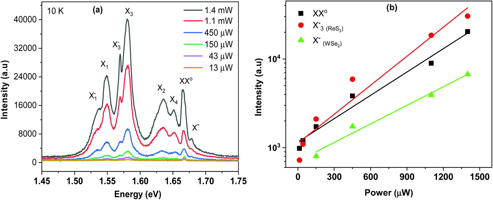 | ||
| Fig. 3 (a) Power dependent PL of the heterostructure at 10 K. (b) Semi-log plot of the observed intensities as a function of the excitation power. | ||
Therefore, the charge species act as polarized excitons and trions. The confinement due to anisotropic screening field pronounced the mixed states (bright and semi-dark) in biexcitons due to electron–electron intervalley scattering as reported earlier in.34 It is further observed in this heterostructure that the PL intensity of the neutral exciton (X°) of WSe2 is significantly quenched. This quenching effect arises from the efficient charge transfer across the heterojunction (electrons to ReS2) which in turn originates from the type-II band alignment, schematically shown in Fig. 1(c). The type II band alignment for this material system was already predicted by DFT calculations.35,36 It can be further elucidated from the spectra that the enhanced XX° is due to the change of the electron mobility under local confinement. The band off-set in the conduction band minimum (CBM) is 0.93 eV and is, hence, larger than the thermal vibrational energy of ∼0.02 meV (phonon mode) at room temperature. The band off-set in the valence band (VBM) is ∼1.03 eV. The emission from the interlayer charge transfer exciton should appear at an energy which is beyond our detector's limit. At the room temperature, the excitonic properties of single-layer and few-layer TMDCs are largely influenced by phonon interactions. To obtain sharp and well-resolved excitonic features we perform PL measurements at low temperature (∼10 K). The excitation light was circularly polarized to obtain uniform excitation in all possible directions. The PL spectra shown in Fig. 2(b) reveal eight emission peaks corresponding to different excitonic features of the heterostructure. The spectra exhibit two higher energy peaks at 1.66 eV and 1.68 eV attributed to the bi-exciton (XX°) and the charged exciton (X−) of WSe2, respectively.
At low temperatures, the localized states thermalize more easily than excitons and trions and a significant amount of charge carriers are trapped in these localized states. This has also been reported earlier.37 At the same time the directional screening from the underlying substrate also forces these carriers to remain in these localized states. There are four exciton peaks at 1.55, 1.58, 1.63 and 1.64 eV related to ReS2, designated as X1, X3, X2 and X4, respectively. The additional peaks X3 and X4 originate from the splitting of excitonic states due to the electron–hole exchange interactions.38 Structural anisotropy resulting from the broken rotational symmetry also contributes to this spin–orbital splitting.
Here, we report for the first time the observation of negatively charged trions of ReS2 (X1− and X3−) in an ungated structure, shown in Fig. 2(b). These newly observed trion peaks are referred to as X1− and X3− and appear at 1.536 eV and 1.572 eV, respectively. They are negatively charged due to the charge transfer-induced electron accumulation in ReS2. The trion peaks are located approximately 18 meV and 15 meV below their respective neutral exciton peaks corresponding to the trion binding energies. These values agree well with previous observations.39 The efficient transfer of charge carriers across the heterostructure is also the reason for the suppression of the neutral exciton (X°) in WSe2. The emission intensity of the WSe2 bi-exciton is much higher than that of both the trion (X−) and the neutral exciton (X°), which we attribute to the directional dielectric-screening-induced exciton localization arising from the underlaying ReS2. This peculiarity has not been observed in previous studies on an isolated WSe2 monolayer.40–42 The enhanced emission is due to the change of screening to a directional environment in this heterostructure.
To clarify the nature of the of individual PL peaks power-dependent photoluminescence measurements are performed. The spectra in Fig. 3 along with a plot of the corresponding intensities confirms the assignment of the peaks to biexciton XX° and trion X− of WSe2 which shows almost linear behaviour with reference to excitation power. The charged trion (X3−) of ReS2 shows nearly quadratic trend. These bi-excitons evolve from two identical neutral excitons with a Bohr radius exactly equal to that of a single exciton (∼1 nm) and separated by ∼3–4 nm.43 Under suitable conditions, these four-body quasiparticles would thus be a strong channel for light emission. Such many body excitonic correlated states favor new quantum properties such as exciton condensates. It could be interesting to produce coherent photons by utilizing these correlated excitons.44 Furthermore, low-temperature PL spectra show two further excitons, designated as X2 and X4, that are close to each other (separated by ∼12 meV). They have a weaker oscillator strength and therefore disappear at higher temperatures.
3.2 Polarization-resolved Photoluminescence
The ReS2 crystal is anisotropic and therefore the PL shows a pronounced polarization dependence. The two neutral polarized excitons in ReS2, namely X1 and X2 have been reported earlier in a single layer and in few-layer samples.45–47 Since, we have a heterostructure we observe here the additional excitons X3 and X4. In the following, we investigate their anisotropic nature using an additional polarizer in front of the detector. Fig. 4(a) shows the polarized PL emission as a function of the polarizer angle. Another representation is the 2D contour plot shown in Fig. 4(b). In this plot the dependence of exciton and trion resonances can clearly be seen for a complete 360° turn of the analyser.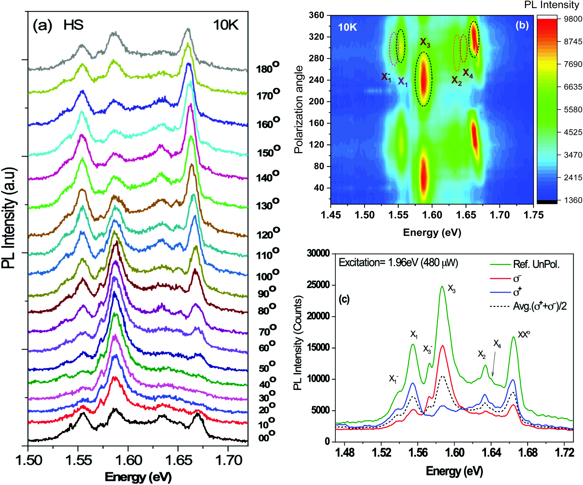 | ||
| Fig. 4 (a). Polarization-resolved PL spectra of the WSe2/ReS2 heterostructure at 10 K. The detection angle varies between 0° to 180° (b). 2D contour plot of PL spectra with polarization angle (θ). (c). The right- and left-handed circular polarization PL spectra. | ||
We also study the degree of polarization of the light from the heterostructure by luminescence measurements employing right-handed and left-handed circular polarized excitation and kept the detection angle fixed, so that the orthogonal helicities are obtained as (σ+) and (σ−). Fig. 4(c) shows that the excitons X1 and X3 are more sensitive to (σ+) and (σ−) polarizations, respectively. The exciton and trion of same orientation are very much consistent with one type of circular polarization. One possible reason would be partial excitation of electron–hole pairs in valleys of dark states XD of localized charge carriers in the respective exciton X1 or X3. The variation in the degree of polarization can also be attributed to a variable oscillator strength and its electron–phonon coupling strength. The comparative low emission signal from X2 and X4 excitons is expected because of lower oscillator strength compared to X1 and X3 excitons as revealed in the temperature dependent PL spectra. The polar plots for the prominent excitonic features of the heterostructure are presented in Fig. 5 as a function of detection angle θ. The exciton X1(X3) as well as the negative trion X1−(X3−) emission exhibits a double-lobed shape, oriented at 63° with respect to each other, corresponding to the angle between a and b-axis of ReS2. This polarization resolved peaks emerge from the splitting of singlet and triplet states; the broken rotational symmetry and structural anisotropy are the reasons for such splitting. The excitonic signal stems primarily from non-degenerate direct excitons.45 The corresponding trions also exhibit a strongly linearly polarized emission of the same orientation. This behaviour suggests the spread of the anisotropic trion wavefunction, which is primarily elongated along and perpendicular to the b-axis for the X1−(X3−) trion.
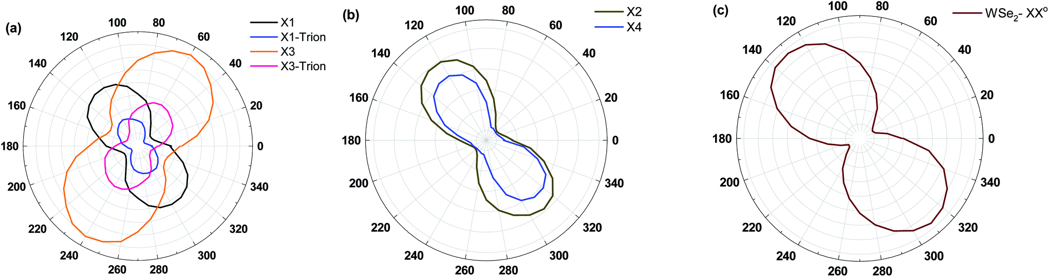 | ||
| Fig. 5 Polar plot of integrated PL intensities for the WSe2/ReS2 heterostructure at 10 K. (a) Intensity of the PL emission from the exciton and trion of ReS2 (X1 and X3, respectively) as a function of the analyzer angle. (b) Intensity of the PL emission from the X2 and X4 excitons of ReS2. (c) Intensity of the PL emission from bi-excitons in WSe2 (XX°). | ||
The WSe2 localized excitons also show a linear polarization as shown in Fig. 5(c), these excitonic species are well aligned with the underlying directional screening field which is consistent with previous results.47
To illustrate the anisotropic nature of the excitonic wavefunction calculations have been performed (cf. ESI†), the results of which are presented in Fig. 6. In an isotropic material, the wave function of the 1s exciton is circular, whereas in this case it is distinctly elliptical. Unlike conventional TMDs (Mo, W), the rhenium TMDs possess inversion symmetry, which leads to a spin degeneracy of the valence and conduction bands. Previous works have suggested that this gives rise to the strong exchange splitting of the 1s-exciton peak of the ReS2 monolayer. While this calculation is beyond the scope of our analytical methods, we can estimate the exchange splitting by referring to the literature.48
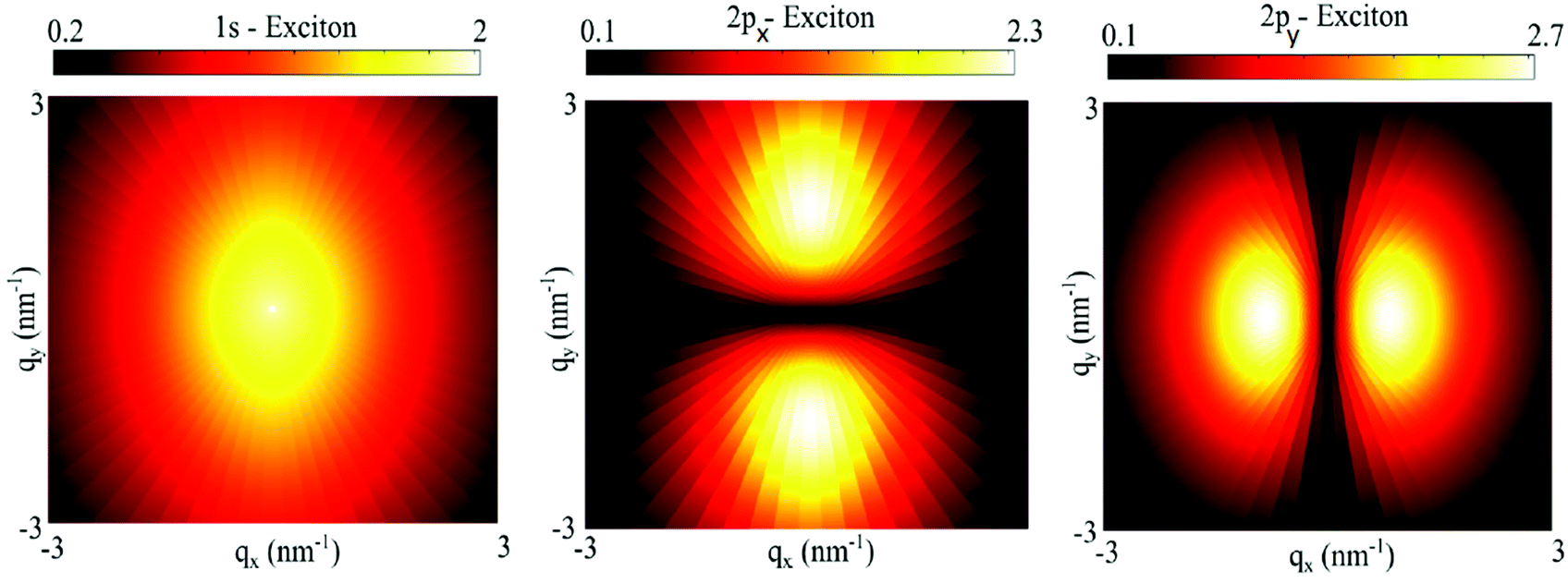 | ||
Fig. 6 Square modulus of excitonic wave functions  for n = 0, 1, 2, for 1s and 2p excitons. for n = 0, 1, 2, for 1s and 2p excitons. | ||
3.3 Temperature dependent Photoluminescence
In order to study the role of phonons, temperature dependent photoluminescence measurements of few layer ReS2, monolayer WSe2 and their heterostructure were performed. The results are presented in Fig. 7. The FL-ReS2 shows the commonly observed exciton X1 at an energy of 1.59 eV with a shoulder at 1.55 eV. In addition, a broad peak is observed at 1.66 eV with an anomalous variation of the intensity as the temperature is increased. This behaviour is attributed to low-lying dark states XD49 recently reported in transition metal dichalcogenides.50–53 As can be seen from Fig. 7(a), the 10 K PL spectrum of the WSe2 monolayer shows well resolved characteristic features of exciton, trion and bi-exciton at 1.72 eV, 1.70 eV and 1.68 eV, respectively.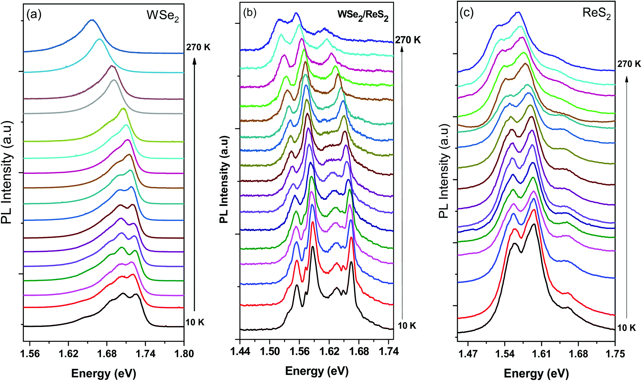 | ||
| Fig. 7 PL spectra measured at different temperatures with a fixed angle of the analyzer, (a). WSe2 (b). Heterostructure of WSe2/ReS2 (c). Few layers of ReS2. | ||
It can be elucidated from the heterostructure PL spectra that the emission arising from bi-excitons of WSe2 has been substantially enhanced as compared to the monolayer. The ReS2 acts as substrate for WSe2 monolayer and its screening field confines the carrier within WSe2, as a result of this confinement the phenomenon of mixed states (bright and semi-dark) is more pronounced in biexcitons due to electron–electron intervalley scattering as reported earlier.34 The lifetime of biexcitons is bit longer than neutral exciton and trion54 which are also responsible for higher quantum yield. Therefore, the confinement due to screening will significantly influence more on biexciton in this heterostructure. Furthermore, it is redshifted by 15 meV. This could be due to further confinement of localized charges because of the screening field underneath. At low temperature these localized states are easy to thermalize than excitons and trions and significant amount of charge carriers are captured in those localized states.37
The X1 exciton which is observed at high temperature splits into two excitons with a narrow linewidth, namely X1 and X3 at low temperature. In addition, one observes corresponding trions as X1− and X3−. The increased electron injection from WSe2 to ReS2 because of charge transfer as well as the encapsulation of ReS2 layers in hBN and WSe2 are the prominent reasons for the emergence of these trions and the narrowing of exciton linewidths. Furthermore, one observes two additional peaks at 1.633 eV and 1.65 eV which we attribute to the X2 and X4 excitons of ReS2, respectively. These two peaks are only resolvable in the temperature range between 10 K and 70 K. At higher temperatures these excitons are thermally populated by absorbing phonons and scattered out of the light cone, as explained by the rate equation model.33 Such phonon modes have been recently observed for ReS2.55 Hence, for the heterostructure we observe a temperature dependent redshift of the peak positions of all exciton species.
We observed Varshni shift for energies with increasing temperature which has been traditionally applied for the bandgap shrinkage in semiconductors;56
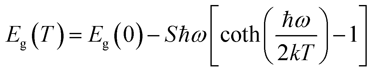
Here, Eg(0) is the resonance energy of the exciton, ℏω is the average phonon energy and S is the electron–phonon coupling constant. Eg(0), S and ℏω are the fitted parameters. Fig. 8(a) reveals that the energy separation between the peaks X1 and X3 of ReS2 is almost constant with temperature. In contrast, the separation between the peaks X2 and X4 is converging with temperature. Fig. 8(b and c) shows the temperature dependent peak positions of the trion X1− and X3− and their corresponding neutral excitons. The insets show the original peak positions, the main figures show the energy difference between exciton and trion. The trion X3− shows a larger energy shift than X1− because it lies in a plane having different dipole moment which is more aligned towards b-axis (∼25°). The linearly polarized emission of the trion in a quantum confined quasi-1D system like this suggests an anisotropic trion wavefunction57 as discussed earlier. This also enhances the Coulomb interaction between charge carriers.58–60
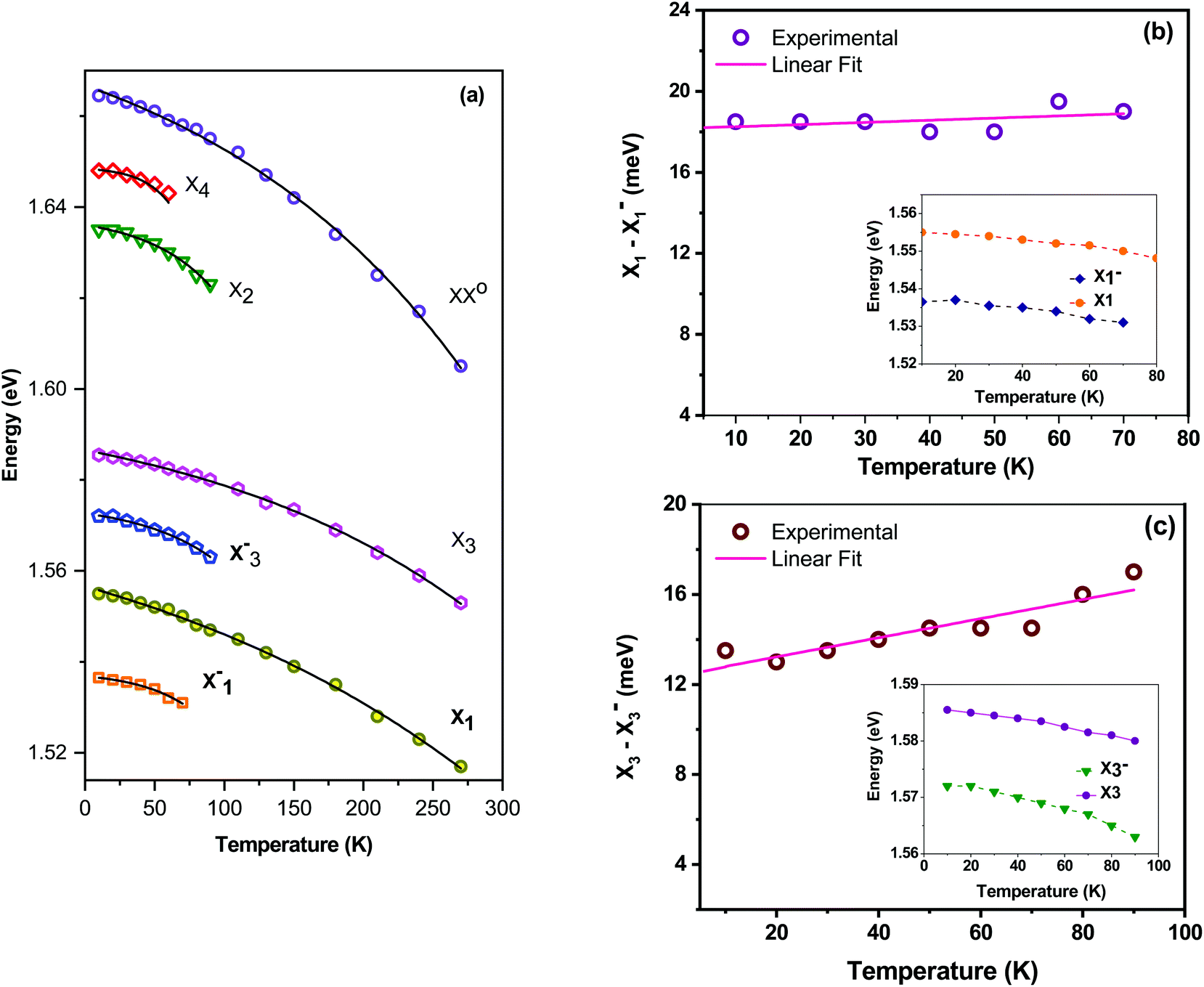 | ||
| Fig. 8 (a). Temperature dependent shift of the excitonic peak positions of the heterostructure. Energy separation between exciton and trion for (b). X1 (c). X3. | ||
3.4 Exciton binding energy in fractional dimension
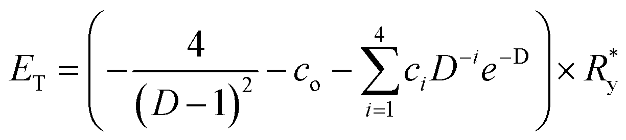
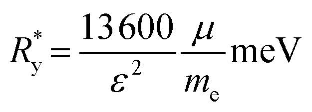
To get an insight into the exciton and trion binding energies for FL-ReS2 with variable dielectric constant, a theoretical analysis is implemented. Numerous techniques are available to estimate the exciton and trion binding energies in quasi-2D materials:60–62e.g. the diffusion Monte Carlo method63 and the boundary matching matrix method.60,63 Following these approaches, we can obtain an estimate for the binding energies. The binding energies of exciton (Eex) and trion (ET) were calculated using the following equations.65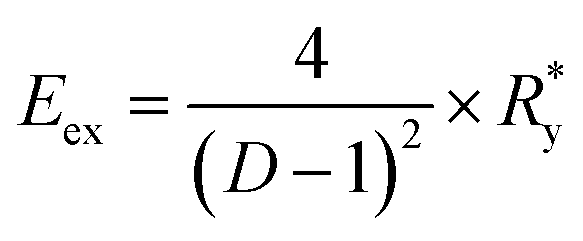
Here Dex and DT are the effective dimension of the exciton and trion, respectively. ε is the dielectric coefficient and  is the effective Rydberg,64
The effective dimension of the trion is slightly smaller than that of the exciton. To keep the calculation simple, we approximate D = Dex = DT. The coefficients ci=1–465 are based on a Monte Carlo study of charged excitons and are described in the ESI (Table S1†). Employing these equations and parameters, we estimated exciton and trion binding energies as a function of fractional dimension for a unique dielectric constant. The result of this calculation is presented in Fig. 9. Based on two dielectric constants of ReS2 along and perpendicular to the b-axis64,66 the exciton and trion wavefunction is elongated in two directions. The excitons which are along b-axis have higher energy as compared to excitons which are confined in a perpendicular direction. A similar behaviour can also be seen for the corresponding trions. The obtained exciton binding energy in ReS2 is slightly higher than reported for other TMDs.67,68 This also supports its quasi-1D nature and agrees with the already reported binding energy.69 It can also be seen that the binding energies of exciton and trion increase with the decrease of the fractional dimension D.
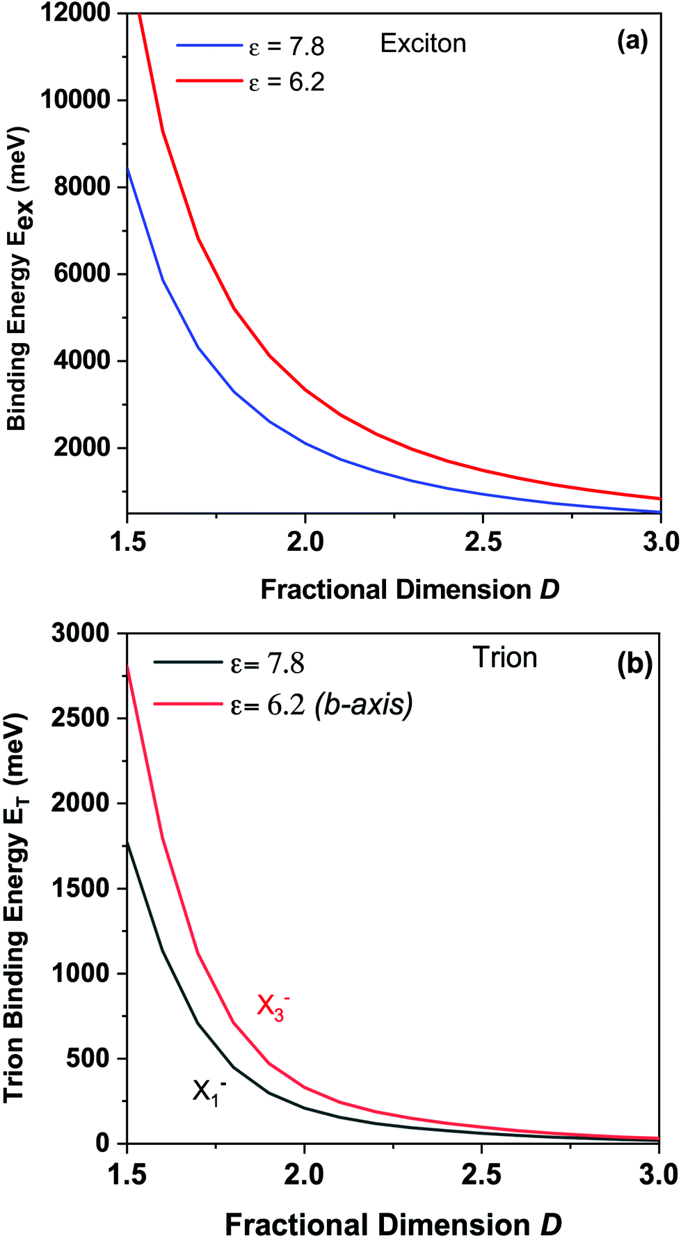 | ||
| Fig. 9 The calculated binding energy for ReS2 as a function of effective dimension D for (a). Exciton (b). Trion. | ||
To draw a comparison of our results obtained on samples with substrates to the exciton binding energy which one would expect for an isolated layer of ReS2, we theoretically calculated the binding energies of excitonic states of a free-standing monolayer using the Wannier equation. The calculated binding energy for the 1s exciton is 859 meV (see ESI Fig. S3†).
4. Conclusions
We have successfully demonstrated the charge transfer exciton in an ungated WSe2/ReS2 heterostructure. We have also observed trions which have thus far only been observed experimentally in a gated structure. Two additional peaks are evident in the luminescence spectrum of ReS2, they are accompanied by two luminescence maxima which we attribute to spin degenerate excitons of ReS2. Polarization-resolved spectra reveal distinct orientations of these excitons and of trions which are elongated in the same orientation as the excitons. The distorted 1T structure of anisotropic ReS2 favours the directional screening due to the existence of variable dielectric constants. The high exciton and trion binding energies also confirm their strongly confined quasi-1D nature. Moreover, ReS2 acts as an optically patterned substrate for the top WSe2 monolayer. Consequently, the WSe2 excitons show a polarized behaviour which differs from their intrinsic properties. Our observations provide new insight into the many-body physics in optically excited states of anisotropic van der Waals systems which are promising materials for optoelectronic devices, including polarization sensitive switches and spin manipulated devices.Conflicts of interest
There are no conflicts to declare.Acknowledgements
We acknowledge the group of Prof. Gregor Witte for providing the AFM image (Fig. S2†). In addition, we acknowledge support from the Collaborative Research Center SFB 1083 funded by the Deutsche Forschungsgemeinschaft and the European Union's Horizon 2020 Research and Innovation Program under grant agreement no. 881603 (Graphene Flagship). M. Adel Aly acknowledges support from the Egyptian Ministry of Higher Education and Scientific Research and Deutsche Akademische Austaush Dienst (DAAD). Further we acknowledge the support by the Alexander von Humboldt (AvH) foundation via a research grant in the Georg Förster fellowship program.References
- A. K. Geim and K. S. Novoselov, The rise of graphene, Nat. Mater., 2007, 6, 183–192 CrossRef CAS PubMed.
- H. Chen, X. Wen and J. Zhang, et al., Ultrafast formation of interlayer hot excitons in atomically thin MoS2/WS2 heterostructures, Nat. Commun., 2016, 7, 12512 CrossRef CAS PubMed.
- Q. Zhao, Y. Guo, Y. Zhou, Z. Yao, Z. Ren, J. Bai and X. Xu, Band alignments and heterostructures of monolayer transition metal trichalcogenides MX3 (M = Zr, Hf; X = S, Se) and dichalcogenides MX2 (M = Tc, Re; X=S, Se) for solar applications, Nanoscale, 2018, 10, 3547–3555 RSC.
- A. Koitzsch, A.-S. Pawlik, C. Habenicht, T. Klaproth, R. Schuster, B. Büchner and M. Knupfer, Nonlocal dielectric function and nested dark excitons in MoS2, npj 2D Mater. Appl., 2019, 3, 41 CrossRef.
- W. Gang, C. Alexey, M. G. Mikhail, F. H. Tony, M. Xavier, A. Thierry and U. Bernhard, Excitons in atomically thin transition metal dichalcogenides, Rev. Mod. Phys., 2018, 90, 021001 CrossRef.
- T. Mueller and E. Malic, Exciton physics and device application of two-dimensional transition metal dichalcogenide semiconductors, npj 2D Mater. Appl., 2018, 2, 29 CrossRef.
- X. Hui, D. Yunyun, K. Wonjae, W. Yadong, B. Xueyin, Q. Mei, H. Kari, L. Harri and S. Zhipei, High photoresponsivity and broadband photodetection with a band-engineered WSe2/SnSe2 heterostructure, Nanoscale, 2019, 11, 3240 RSC.
- D. Jariwala, S. L. Howell, K. S. Chen, J. Kang, V. K. Sangwan, S. A. Filippone, R. Turrisi, T. J. Marks, L. J. Lauhon and M. C. Hersam, Hybrid, Gate-Tunable, van der Waals p–n Heterojunctions from Pentacene and MoS2, Nano Lett., 2016, 16, 497–503 CrossRef CAS PubMed.
- M. Bernardi, M. Palummo and J. C. Grossman, Extraordinary sunlight absorption and one nanometer thick photovoltaics using two-dimensional monolayer materials, Nano Lett., 2013, 13, 3664–3670 CrossRef CAS PubMed.
- K. F. Mak, C. Lee, J. Hone, J. Shan and T. F. Heinz, Atomically thin MoS2: a new direct-gap semiconductor, Phys. Rev. Lett., 2010, 105, 136805 CrossRef PubMed.
- D. Wu, J. Guo, J. Du, C. Xia, L. Zeng, Y. Tian, Z. Shi, Y. Tian, X. J. Li, Y. H. Tsang and J. Jie, Highly Polarization-Sensitive, Broadband, Self-Powered Photodetector Based on Graphene/PdSe2/Germanium Heterojunction, ACS Nano, 2019, 13(9), 9907–9917 CrossRef CAS PubMed.
- M. R. Molas, A. O. Slobodeniuk, K. Nogajewski, M. Bartos, Ł. Bala, A. Babiński, K. Watanabe, T. Taniguchi, C. Faugeras and M. Potemski, Energy Spectrum of Two-Dimensional Excitons in a Nonuniform Dielectric Medium, Phys. Rev. Lett., 2019, 123, 136801 CrossRef CAS PubMed.
- K. Noori, N. L. Q. Cheng, F. Xuan and S. Y. Quek, Dielectric screening by 2D substrates, 2D Mater., 2019, 6, 035036 CrossRef CAS.
- M. Le Ster, T. Maerkl, P. J. Kowalczyk and S. A. Brown, Moiré patterns in van der Waals heterostructures, Phys. Rev. B, 2019, 99, 075422 CrossRef.
- M. Förg, L. Colombier, R. K. Patel, J. Lindlau, A. D. Mohite, H. Yamaguchi, M. M. Glazov, D. Hunger and A. Högele, Cavity-control of interlayer excitons in van der Waals heterostructures, Nat. Commun., 2019, 10, 3697 CrossRef PubMed.
- A. Ciarrocchi, D. Unuchek, A. Avsar, K. Watanabe, T. Taniguchi and A. Kis, Polarization switching and electrical control of interlayer excitons in two-dimensional van der Waals heterostructures, Nat. Photonics, 2018, 13, 131–136 CrossRef PubMed.
- S. Brem, C. Linderälv, P. Erhart and E. Malic, Tunable Phases of Moiré Excitons in van der Waals Heterostructures, Nano Lett., 2020, 20, 8534–8540 CrossRef CAS PubMed.
- P. Merkl, F. Mooshammer, P. Steinleitner, A. Girnghuber, K. Q. Lin, P. Nagler, J. Holler, C. Schüller, J. M. Lupton, T. Korn, S. Ovesen, S. Brem, E. Malic and R. Huber, Ultrafast transition between exciton phases in van der Waals heterostructures, Nat. Mater., 2019, 18, 691–696 CrossRef CAS PubMed.
- P. Zereshki, P. Yao, D. He, Y. s. Wang and H. Zhao, Interlayer charge transfer in ReS2/WS2 van der Waals heterostructures, Phys. Rev. B, 2019, 99, 195438 CrossRef CAS.
- D. Rhodes, S. H. Chae, R. Ribeiro-Palau and J. Hone, Disorder in van der Waals heterostructures of 2D materials, Nat. Mater., 2019, 18, 541–549 CrossRef CAS PubMed.
- V. Ongun Özçelik, J. G. Azadani, C. Yang, S. J. Koester and T. Low, Band alignment of two-dimensional semiconductors for designing heterostructures with momentum space matching, Phys. Rev. B, 2016, 94, 035125 CrossRef.
- N. R. Wilson, P. V. Nguyen, K. Seyler, P. Rivera, A. J. Marsden, Z. P. L. Laker, G. C. Constantinescu, V. Kandyba, A. Barinov, N. D. M. Hine, X. Xu and D. H. Cobden, Determination of band offsets, hybridization, and exciton binding in 2D semiconductor heterostructures, Sci. Adv., 2017, 3, e160183 Search PubMed.
- G. Berghäuser, I. Bernal-Villamil, R. Schmidt, R. Schneider, I. Niehues, P. Erhart, S. M. de Vasconcellos, R. Bratschitsch, A. Knorr and E. Malic, Inverted valley polarization in optically excited transition metal dichalcogenides, Nat. Commun., 2018, 9, 971 CrossRef PubMed.
- R. He, J.-A. Yan, Z. Yin, Z. Ye, G. Ye, J. Cheng, J. Li and C. H. Lui, Coupling and Stacking Order of ReS2 Atomic Layers Revealed by Ultralow-Frequency Raman Spectroscopy, Nano Lett., 2016, 16, 1404–1409 CrossRef CAS PubMed.
- M. Saeed, W. Uddin, A. S. Saleemi, M. Hafeez, M. Kamil, I. A. Mir, Sunila, R. Ullah, S. U. Rehman and Z. Ling, Optoelectronic properties of MoS2-ReS2 and ReS2-MoS2 heterostructures, Phys. B, 2020, 577, 411809 CrossRef CAS.
- T. Zhang, B. Jiang, Z. Xu1, R. G. Mendes, Y. Xiao, L. Chen, L. Fang, T. Gemming, S. Chen, M. H. Rummeli and L. Fu, Twinned growth behavior of two-dimensional materials, Nat. Commun., 2016, 7, 13911 CrossRef CAS PubMed.
- W. Zhu, X. Wei, F. Yan, Q. Lv, C. Hu and K. Wang, Broadband polarized photodetector based on p-BP/n-ReS2 heterojunction, J. Semicond., 2019, 40, 092001 CrossRef CAS.
- S. Kallatt, S. Das, S. Chatterjee and K. Majumdar, Interlayer charge transport controlled by exciton–trion coherent coupling, npj 2D Mater. Appl., 2019, 3, 15 CrossRef.
- T. Godde, D. Schmidt, J. Schmutzler, M. Aßmann, J. Debus, F. Withers, E. M. Alexeev, O. Del Pozo-Zamudio, O. V. Skrypka, K. S. Novoselov, M. Bayer and A. I. Tartakovskii, Exciton and trion dynamics in atomically thin MoSe2 and WSe2: Effect of localization, Phys. Rev. B, 2016, 94, 165301 CrossRef.
- Z. Li, T. Wang, Z. Lu, C. Jin, Y. Chen, Y. Meng, Z. Lian, T. Taniguchi, K. Watanabe, S. Zhang, D. Smirnov and S.-F. Shi, Revealing the biexciton and trion-exciton complexes in BN encapsulated WSe2, Nat. Commun., 2018, 9, 3719 CrossRef PubMed.
- E. Liu, J. van Baren, Z. Lu, M. M. Altaiary, T. Taniguchi, K. Watanabe, D. Smirnov and C. H. Lui, Gate Tunable Dark Trions in Monolayer WSe2, Phys. Rev. Lett., 2019, 123, 027401 CrossRef CAS PubMed.
- Y. Miyauchi, S. Konabe, F. Wang, W. Zhang, A. Hwang, Y. Hasegawa, L. Zhou, S. Mouri, M. Toh, G. Eda and K. Matsuda, Evidence for line width and carrier screening effects on excitonic valley relaxation in 2D semiconductors, Nat. Commun., 2018, 9, 2598 CrossRef PubMed.
- A. Dhara, D. Chakrabarty, P. Das, A. K. Pattanayak, S. Paul, S. Mukherjee and S. Dhara, Additional excitonic features and momentum-dark states in ReS2, Phys. Rev. B, 2020, 102, 161404 (R) CrossRef.
- M. Danovich, V. Zólyomi and V. I. Fal’ko, Dark trions and biexcitons in WS2 and WSe2 made bright by e-e scattering, Sci. Rep., 2017, 7, 45998 CrossRef CAS PubMed.
- S. Tongay, H. Sahin, C. Ko, A. Luce, W. Fan, K. Liu, J. Zhou, Y.-S. Huang, C.-H. Ho, J. Yan, D. F. Ogletree, S. Aloni, J. Ji, S. Li, J. Li, F. M. Peeters and J. Wu, Monolayer behaviour in bulk ReS2 due to electronic and vibrational decoupling, Nat. Commun., 2014, 5, 3252 CrossRef PubMed.
- J. L. Webb, L. S. Hart and D. Wolverson, Electronic band structure of ReS2 by high-resolution angle-resolved photoemission spectroscopy, Phys. Rev. B, 2017, 96, 115205 CrossRef.
- J. Huang, T. B. Hoang and M. H. Mikkelsen, Probing the origin of excitonic states in monolayer WSe2, Sci. Rep., 2016, 6, 22414 CrossRef CAS PubMed.
- R. Oliva, M. Laurien, F. Dybala, J. Kopaczek and Y. Qin, et al., Pressure dependence of direct optical transitions in ReS2 and ReSe2, npj 2D Mater. Appl., 2019, 3, 20 CrossRef.
- T. Yan, X. Qiao, X. Liu, P. Tan and X. Zhang, Photoluminescence properties and exciton dynamics in monolayer WSe2, Appl. Phys. Lett., 2014, 105, 101901 CrossRef.
- T. Yan, X. Qiao, X. Liu, P. Tan and X. Zhang, Photoluminescence properties and exciton dynamics in monolayer WSe2, Appl. Phys. Lett., 2014, 105, 101901 CrossRef.
- J. Huang, T. B. Hoang and M. H. Mikkelsen, Probing the origin of excitonic states in monolayer WSe2, Sci. Rep., 2016, 6, 22414 CrossRef CAS PubMed.
- M. Barbone, A. R. P. Montblanch, D. M. Kara, C. Palacios-Berraquero, A. R. Cadore, D. De Fazio, B. Pingault, E. Mostaani, H. Li, B. Chen, K. Watanabe, T. Taniguchi, S. Tongay, G. Wang, A. C. Ferrari and M. Atatüre, Charge tuneable biexciton complexes in monolayer WSe2, Nat. Commun., 2018, 9, 3721 CrossRef PubMed.
- Y. You, X. X. Zhang, T. C. Berkelbach, M. S. Hybertsen, D. R. Reichman and T. F. Heinz, Observation of biexcitons in monolayer WSe2, Nat. Phys., 2015, 11, 477 Search PubMed.
- O. B. Aslan, D. A. Chenet, A. M. van der Zande, J. C. Hone and T. F. Heinz, Linearly Polarized Excitons in Single and Few-Layer ReS2 Crystals, ACS Photonics, 2016, 3, 96–101 Search PubMed.
- J. M. Urban, M. Baranowski, A. Kuc, Ł. Kłopotowski, A. Surrente, Y. Ma, D. Włodarczyk, A. Suchocki, D. Ovchinnikov and T. Heine, Non-equilibrium anisotropic excitons in atomically thin ReS2, 2D Mater., 2019, 6, 015012 Search PubMed.
- S. Sim, D. Lee, M. Noh, S. Cha, C. H. Soh, J. H. Sung, M.-H. Jo and H. Choi, Selectively tunable optical Stark effect of anisotropic excitons in atomically thin ReS2, Nat. Commun., 2016, 7, 13569 Search PubMed.
- L. H. Li, T. Tian, Q. Cai, C.-J. Shih and E. J. G. Santos, Asymmetric electric field screening in van der Waals heterostructures, Nat. Commun., 2018, 9, 1271 Search PubMed.
- R. Oliva, M. Laurien, F. Dybala, J. Kopaczek, Y. Qin, S. Tongay, O. Rubel and R. Kudrawiec, Pressure dependence of direct optical transitions in ReS2 and ReSe2, npj 2D Mater. Appl., 2019, 3, 20 Search PubMed.
- M. R. Molas, C. Faugeras, A. O. Slobodeniuk, K. Nogajewski, M. Bartos, D. M. Basko and M. Potemski, Brightening of dark excitons in monolayers of semiconducting transition metal dichalcogenides, 2D Mater., 2017, 4, 021003 Search PubMed.
- A. Arora, N. K. Wessling, T. Deilmann, T. Reichenauer, P. Steeger, P. Kossacki, M. Potemski, S. M. de Vasconcellos, M. Rohlfing and R. Bratschitsch, Dark trions govern the temperature-dependent optical absorption and emission of doped atomically thin semiconductors, Phys. Rev. B, 2020, 101, 241413 (R) CrossRef.
- M. Selig, G. Berghäuser, M. Richter, R. Bratschitsch, A. Knorr and E. Malic, Dark and bright exciton formation, thermalization, and photoluminescence in monolayer transition metal dichalcogenides, 2D Mater., 2018, 5(3), 035017 CrossRef.
- E. Malic, M. Selig, M. Feierabend, S. Brem, D. Christiansen, F. Wendler, A. Knorr and G. Berghäuser, Dark excitons in transition metal dichalcogenides, Phys. Rev. Mater., 2018, 2, 014002 CrossRef CAS.
- S. Brem, A. Ekman, D. Christiansen, F. Katsch, M. Selig, C. Robert, X. Marie, B. Urbaszek, A. Knorr and E. Malic, Phonon-Assisted Photoluminescence from Indirect Excitons in Monolayers of Transition-Metal Dichalcogenides, Nano Lett., 2020, 20, 2849 CrossRef CAS PubMed.
- Y. You, X. X. Zhang, T. C. Berkelbach, M. S. Hybertsen, D. R. Reichman and T. F. Heinz, Observation of biexcitons in monolayer WSe2, Nat. Phys., 2015, 11, 477–481 Search PubMed.
- A. McCreary, J. R. Simpson, Y. Wang, D. Rhodes, K. Fujisawa, L. Balicas, M. Dubey, V. H. Crespi, M. Terrones and A. R. H. Walker, Intricate Resonant Raman Response in Anisotropic ReS2, Nano Lett., 2017, 17, 5897 CrossRef CAS PubMed.
- K. P. O'Donnell and X. Chen, Temperature dependence of semiconductor band gaps, Appl. Phys. Lett., 1991, 58, 2924 CrossRef.
- R. Matsunaga, K. Matsuda and Y. Kanemitsu, Observation of Charged Excitons in Hole-Doped Carbon Nanotubes Using Photoluminescence and Absorption Spectroscopy, Phys. Rev. Lett., 2011, 106, 037404 CrossRef PubMed.
- A. Sharma, H. Yan, L. Zhang, X. Sun, B. Liu and Y. Lu, Highly Enhanced Many-Body Interactions in Anisotropic 2D Semiconductors, Acc. Chem. Res., 2018, 51, 1164 CrossRef CAS PubMed.
- A. S. Rodin, A. Carvalho and A. H. Castro Neto, Excitons in anisotropic two-dimensional semiconducting crystals, Phys. Rev. B: Condens. Matter Mater. Phys., 2014, 90, 075429 CrossRef CAS.
- B. Ganchev, N. Drummond, I. Aleiner and V. Fal’ko, Three-Particle Complexes in Two-Dimensional Semiconductors, Phys. Rev. Lett., 2015, 114, 107401 CrossRef PubMed.
- A. Thilagam, Exciton Complexes in Low Dimensional Transition Metal Dichalcogenides, J. Appl. Phys., 2014, 116, 053523 CrossRef.
- W. Ruan, K. Chan, H. Ho, R. Zhang and E. Pun, Hyper spherical Approach for Charged Excitons in Quantum Wells, Phys. Rev. B: Condens. Matter Mater. Phys., 1999, 60, 5714 CrossRef CAS.
- R. Needs, M. Towler, N. Drummond and P. L. Ríos, Continuum Variational and Diffusion Quantum Monte Carlo Calculations, J. Phys.: Condens. Matter, 2010, 22, 023201 CrossRef CAS PubMed.
- A. Thilagam, Stark shifts of excitonic complexes in quantum wells, Phys. Rev. B: Condens. Matter Mater. Phys., 1997, 56, 4665 CrossRef CAS.
- T. F. Rønnow, T. G. Pedersen, B. Partoens and K. K. Berthelsen, Variational Quantum Monte Carlo Study of Charged Excitons in Fractional Dimensional Space, Phys. Rev. B: Condens. Matter Mater. Phys., 2011, 84, 035316 CrossRef.
- J. Jadczak, J. Kutrowska-Girzycka, T. Smoleński, P. Kossacki, Y. S. Huang and L. Bryja, Exciton binding energy and hydrogenic Rydberg series in layered ReS2, Sci. Rep., 2019, 9, 1578 CrossRef CAS PubMed.
- M. M. Ugeda, A. J. Bradley, S.-F. Shi, F. H. da Jornada, Y. Zhang, D. Y. Qiu, W. Ruan, S.-K. Mo, Z. Hussain, Z.-X. Shen, F. Wang, S. G. Louie and M. F. Crommie, Giant Bandgap Renormalization and Excitonic Effects in a Monolayer Transition Metal Dichalcogenide Semiconductor, Nat. Mater., 2014, 13, 1091–1095 CrossRef CAS PubMed.
- Z. Ye, T. Cao, K. O'Brien, H. Zhu, X. Yin, Y. Wang, S. G. Louie and X. Zhang, Probing Excitonic Dark States in Single-Layer Tungsten Disulfide, Nature, 2014, 513, 214–218 CrossRef CAS PubMed.
- A. Sharma, H. Yan, L. Zhang, X. Sun, B. Liu and Y. Lu, Highly Enhanced Many-Body Interactions in Anisotropic 2D Semiconductors, Acc. Chem. Res., 2018, 51(5), 1164–1173 CrossRef CAS PubMed.
Footnote |
| † Electronic supplementary information (ESI) available: Theoretical model and DFT input for calculation of exciton binding energy and wavefunction, Raman spectroscopy for quantification of ReS2 layers. See DOI: https://doi.org/10.1039/d2nr01973f |
| This journal is © The Royal Society of Chemistry 2022 |