
 Open Access Article
 This Open Access Article is licensed under a Creative Commons Attribution-Non Commercial 3.0 Unported Licence
Combined spin filtering actions in hybrid magnetic junctions based on organic chains covalently attached to graphene†
Pascal
Martin
 a,
Bruno
Dlubak
*b,
Richard
Mattana
b,
Pierre
Seneor
b,
Marie-Blandine
Martin
b,
Théo
Henner‡
c,
Florian
Godel
b,
Anke
Sander
b,
Sophie
Collin
b,
Linsai
Chen
a,
Stéphan
Suffit
c,
François
Mallet
c,
Philippe
Lafarge
c,
Maria Luisa
Della Rocca
c,
Andrea
Droghetti
*d and
Clément
Barraud
*c
a,
Bruno
Dlubak
*b,
Richard
Mattana
b,
Pierre
Seneor
b,
Marie-Blandine
Martin
b,
Théo
Henner‡
c,
Florian
Godel
b,
Anke
Sander
b,
Sophie
Collin
b,
Linsai
Chen
a,
Stéphan
Suffit
c,
François
Mallet
c,
Philippe
Lafarge
c,
Maria Luisa
Della Rocca
c,
Andrea
Droghetti
*d and
Clément
Barraud
*c
aUniversité Paris Cité, Laboratoire ITODYS, CNRS, UMR 7086, 75013 Paris, France
bUnité Mixte de Physique, CNRS, Thales, Université Paris-Saclay, 91767 Palaiseau, France. E-mail: bruno.dlubak@cnrs-thales.fr
cUniversité Paris Cité, Laboratoire Matériaux et Phénomènes Quantiques, CNRS, UMR 7162, 75013 Paris, France. E-mail: clement.barraud@u-paris.fr
dSchool of Physics and CRANN, Trinity College, Dublin 2, Ireland
First published on 22nd August 2022
Abstract
We present a bias-controlled spin-filtering mechanism in spin-valves including a hybrid organic chain/graphene interface. Wet growth conditions of oligomeric molecular chains would usually lead, during standard CMOS-compatible fabrication processes, to the quenching of spintronics properties of metallic spin sources due to oxidation. We demonstrate by X-ray photoelectron spectroscopy that the use of a protective graphene layer fully preserves the metallic character of the ferromagnetic surface and thus its capability to deliver spin polarized currents. We focus here on a small aromatic chain of controllable lengths, formed by nitrobenzene monomers and derived from the commercial 4-nitrobenzene diazonium tetrafluoroborate, covalently attached to the graphene passivated spin sources thanks to electroreduction. A unique bias dependent switch of the spin signal is then observed in complete spin valve devices, from minority to majority spin carriers filtering. First-principles calculations are used to highlight the key role played by the spin-dependent hybridization of electronic states present at the different interfaces. Our work is a first step towards the exploration of spin transport using different functional molecular chains. It opens the perspective of atomic tailoring of magnetic junction devices towards spin and quantum transport control, thanks to the flexibility of ambient electrochemical surface functionalization processes.
Introduction
Spintronic circuits, such as widely distributed Magnetic Random Access Memories,1,2 have been developed for further integration in CMOS (Complementary Metal Oxide Semi-conductor) technologies3 as well as for post-CMOS visions, such as low-power spin-logic, stochastic and neuromorphic computing.4–7 Progress along these directions requires optimized material platforms not only to enhance device performances, but, at the same level of importance, also to bring unprecedented functionalities.Organic, uni-, bi- and tri-dimensional materials have been heralded as promising venues8–11 for spintronics because of their atom-by-atom tunable physical properties. To date, several works have successfully demonstrated spin transport through these systems in hybrid spin-valve devices.10,12–15 However only a limited number of organic compounds among the virtually infinite library has been explored for applications proving multifunctionality.10,16,17 Integrating very diverse molecules into spintronics devices stable under ambient conditions is indeed a difficult technological task. Chemical processes such as electrochemical grafting18,19 or self-assembly of monolayers20–22 would in principle represent viable approaches. However, the required wet conditions or the exposure to air during device fabrications processes leads to the oxidation of spin-source electrode materials, such as Ni, Co, Fe and their alloys, thus quenching the spin polarization properties and disrupting device performances. Fabrication protocol has been then developed to circumvent this issue.23 In this article, we propose an alternative approach to introduce electrochemical grafting processes in spintronics devices. We use a graphene layer to protect metallic electrodes against oxidation and preserve thus their capabilities to deliver a spin-polarized current. Nitrobenzene oligomers are then covalently attached onto graphene via a direct C–C bond by electrochemical means demonstrating highly reproducible atomic scale crafting of spintronics transport properties. In particular, we realize and fully characterize Ni/graphene/nitrobenzene oligomers/Co junctions. The measurements display a bias-controlled sharp switch of the sign of the magnetoresistive signal. This sharp switch is very specific to our new device and does not resemble to any previously reported results in organic spin-valves or magnetic tunnel junctions.20,24 It is explained as a combined action of the spin-dependent hybridization between the various materials. Although we use a specific oligomer chain, our technological approach can be applied to electrochemically integrate many different families of molecular compounds onto graphene-protected ferromagnetic electrodes. It therefore offers countless possibilities for improving device performances and for harnessing multifunctional behaviors.
Results and discussion
Fabrication details of organic magnetic junctions based on electrografting wet processes
In Fig. 1, the main steps of our technological process are successively detailed. First, the Ni electrode is patterned on a SiO2/Si wafer using laser lithography and electron beam evaporation. This allows to define Ni lines playing the role of ferromagnetic spin sources in the final structure. In usual magnetic tunnel junction's structures, the barrier material is subsequently grown in situ under vacuum, preserving the metallic surface spin states of the underlying magnetic electrode.14,25 In our approach, the electrografting procedure of organic compounds is a wet process performed in ambient conditions.26,27 We thus need to protect the Ni surface against degradation. We make use of a large scale CVD graphene passivation layer which is known to be impermeable and thus prevent oxidation of metals.28,29 The growth of the graphene layers is achieved by transferring the sample in an adapted cold-wall growth reactor CVD system. The Ni lines exposed to C2H2, act as a catalyzer for the growth of graphene (see Methods).28,30,31 This growth process on Ni spin sources results in a continuous few-layer graphene passivation film. Overall, this process leads to the definition of Ni/Gr lines serving as compatible platforms for electrografting. The next step is the chemical functionalization of the Gr/Ni electrode based on the electroreduction of a diazonium salt.32–34 This process leads to a compact, thin and stable organic film composed of organic chains covalently grafted onto the Gr/Ni substrate.19 To demonstrate the principle of our approach, we chose the prototypical 4-nitrobenzene diazonium tetrafluoroborate molecule (NBD named NB after electrografting) which is the simplest diazonium salt commercially available. Different past studies report the use of NBD as a benchmark to illustrate the grafting of diazonium salts since the presence of nitrophenyl groups can be characterized by electrochemistry and X-ray photoelectron spectroscopy (XPS).35–38 Finally, the evaporation of the Co top electrode can be performed following a standard e-beam evaporation process. | ||
| Fig. 1 Technological steps of the fabrication of a functional organic magnetic junction. A 200 nm-thick patterned Ni spin source electrode is deposited by sputtering over a standard Si/SiO2 substrate. Exposure of C2H2 allows the growth of a large-scale graphene layers on top of the Ni electrode to protect it during further chemical processing. The electrografting procedure is then performed to grow amorphous oligomeric organic chains of NB monomers on top of the graphene protected ferromagnetic electrode spin source. Final device integration is carried out to define a magnetic junction where the Gr/NB heterostructure is contacted by two ferromagnetic electrodes (20 nm of Co is chosen as a top electrode). | ||
The Fig. 2(a) displays the cyclic voltammetry (C–V) of Gr/Ni electrodes in the presence of 4-nitrophenyl diazonium in acetonitrile solution for five cycles. The recorded CV presents a monoelectronic irreversible wave at potential Ep = −0.3 V per SCE. Following that, the first wave disappears and cannot be recovered upon further cycles. The gradual decrease of the current is related to the passivation of the electrode through the grafting of NB radicals onto Gr/Ni surface. This behavior is clearly attributed to the formation of NO2-phenyl (NB) film over the Gr/Ni electrode as usually reported for graphene surfaces39 or for standard metallic surfaces.26,40 Microscopically, each monomer in its radical form is either covalently bonded to the graphene surface locally modifying its hybridization from sp2 to sp3 (ref. 32, 34, 38, 39, 41 and 42) or attached to another monomer already grafted to the graphene surface and thus forming oligomeric chains.43–45
 | ||
| Fig. 2 Electrografting of the molecular chains and preservation of the Ni metallic surface. (a) Cyclic voltammetry of five cycles of Ni/Gr electrodes in a 5 mM NBD solution. Scan rate 100 mV s−1. The chains length can be controlled in a cycle-by-cycle manner allowing tuning the organic barrier thickness in the final structure.26 Inset: schematics of the growth of the NB chains. Each cycle will generate new radical moieties in the solution. (b) XPS Ni 2p spectrum of Gr/Ni electrodes after the growth of the NB molecular chains. This XPS study confirms the preserved metallic nature of the Ni surface even after electrografting due to the protective nature of the impermeable graphene layer. | ||
This process leads to the coverage of the Gr/Ni electrode by a dense and amorphous film of NB chains as widely described in earlier review.18 Previous studies demonstrates that this type of organic layers is very compact (i.e. strongly limiting atomic diffusion) and thus compatible with solid state electronic devices.40,43,46–48 Moreover, the number of cycles or the potential window allow to finely tune the thickness of the deposited organic film as determined by AFM or XPS measurements.26,49,50 Here we focus on a device with an ultrathin NB layers (∼1.3 nm) corresponding to 2 cycles of electrografting) to keep the transport process across the organic NB film in the tunneling regime.26,48
The main difficulty for implementing surface chemistry of ferromagnetic electrodes for spintronics based on ambient and wet chemistry remains the inescapable degradation of the metallic spin source surface due to the high reactivity of transition metals like Co, Ni or Fe and alloys. Indeed, oxidation occurs at the surface and it is widely known to quench the emerging spin polarization.51 Few technological solutions were investigated such as the use of oxide materials as electrodes,52,53 surface pre-cleaning with an appropriate acid23 or a parallel growth/surface reduction by electrochemistry.22,54 Graphene protection was also shown to allow preserving a metallic interface in ambient conditions as demonstrated earlier.28 We investigate here the chemical state of the Ni surface by XPS to assess the pertinence of the proposed graphene passivation after electrografting. As shown in Fig. 2(b), we measure the 2p state of the Ni surface after the grafting process. Strikingly, the XPS study confirm that the Ni surface metallicity is preserved thanks to the graphene protection layer.
Magnetoresistive response of a Ni/graphene/NB/Co magnetic junction
In the following, we present the impact of the integration of the developed stack into a complete spintronic device. Here we focus on the 2-cycles NB film, corresponding to an organic layer thickness of ∼1.3 nm to emphasize the effect. As shown on Fig. 1 (SEM image), micrometric Ni/Gr/NB/Co magnetic junction of 5 × 5 μm2 is fabricated using laser lithography. Here Co (capped by Au) is used as spin analyzer. Fig. 3 shows the typical current–voltage (I–V) characteristics measured at low temperature (T = 2 K). A non-linear behavior with a high (∼100 MΩ) zero-bias electrical resistance was observed. The inset shows the calculated differential conductance which has a parabolic trend. All these signatures are typical of tunneling transport between the two ferromagnetic contacts and are in agreement with previous transport experiments performed on the same molecular chains.46 This demonstrates that the proposed approach indeed allows us to probe transport properties across the organic film. We note that we observe a small rectification (I = +623pA for V = +300 mV and I = −651 pA for V = −300 mV) similar to that found at multilayer graphene/oligomer chain/Au junctions39 and attributed to the molecule-graphene covalent contact.55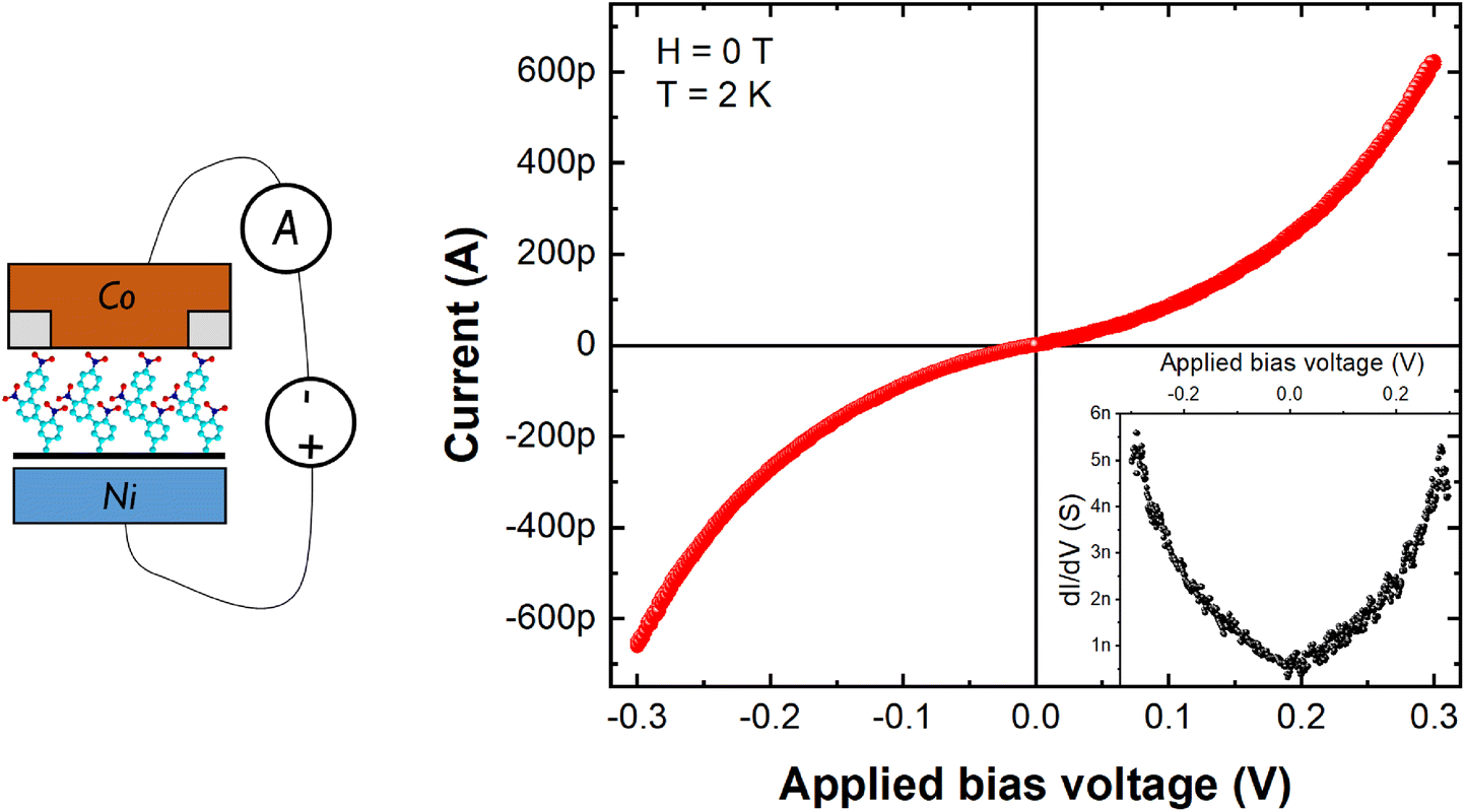 | ||
| Fig. 3 Charge transport characteristics. I–V and dI/dV (inset) of a junction measured across a Ni/Gr/NB (1.3 nm)/Co junction at 2 K revealing high electrical resistance and non-linear tunneling characteristics. A schematic of the measurement configuration is shown on the left. | ||
The use of spin polarizer and analyzer electrodes in our configuration indeed allows to further probe the spin transport properties across the graphene/NB film. Strikingly, as shown in Fig. 4(a), we measure a magnetoresistive (MR) signal MR = −4% at 2 K, defined as:
 | (1) |
 | ||
| Fig. 4 Magnetoresistive signal and its bias voltage dependence. Magnetoresistance of a NB-based organic magnetic junction. (a) A typical negative MR signal as measured at V = +15 mV (T = 2 K). The pink data points and the black data points represent opposite sweep in magnetic field. (b) The MR signal becomes positive at larger bias voltages as measured at V = +30 mV. (c) The overall spin signal amplitude measured as a function of the applied bias revealing a switch in sign of the spin filtering efficiency across the device. | ||
This demonstrates effective spin transport through the NB-based magnetic junction. Note that the sign of the measured MR (for V = +15 mV) for the low-bias measurements is negative as already reported in Ni/Gr/Al2O3/Co magnetic tunnel junctions with Al2O3/Co as spin analyzer.28 Here the extracted emerging spin polarization of the top electrode is defined by the Co/NB hybrid interface and is hence potentially expected to depart from the traditional Al2O3/Co spin analyzer due to hybridization effects.11,15,57
We thus further characterize the spin transport across our organic heterostructure by measuring the MR response at different bias voltages. Surprisingly, in Fig. 4(b) a full reversal of the spin signal at higher voltage V = +30 mV can be observed. This already shows that the studied system is providing a lever for the manipulation of the sign of the interfacial spin polarizations. In Fig. 4(c) we present a more systematic study of the spin signal amplitude and sign as a function of the applied bias voltage. It appears that two different spin transport regimes are available in the hybrid organic junction. At low bias voltages (+25 mV > V > −25 mV), the junction mimics Ni/Gr/Al2O3/Co junctions,28 with a negative MR. However, at higher bias voltages, we observe an abrupt sign change of the MR signal and we thus deduce that, following the Jullière's formula,58 one interface has changed its sign in terms of spin polarization. This reversal is observed for both positive and negative bias voltages. This effect is reminiscent of the expected modulation of the spin property due to hybridization at organic/ferromagnetic metal interfaces15 dubbed “spinterfaces”.59,60 We reveal here an unprecedented extremely sharp control of the sign of the tunneling spin polarization thanks to bias voltage.
Electronic structure of a Ni/Gr/NB/Co junction
To understand spin-filtering across the Ni/Gr/NB/Co junction, we start by carrying out first-principles calculations based on Density Functional Theory (DFT). The simulated device is shown in Fig. 5(a). The molecule is an oligomeric chain composed of three NB units. Three units correspond to a theoretical length of 1.4 nm, which is comparable to the experimental system. The Gr/Ni and the Co electrode are respectively referred to as the bottom and top electrode. The Gr/Ni separation is set equal to the physisorption distance (dNi/graphene = 3.3 Å)61 as there is experimental evidence that the CVD graphene passivation layer realized with our approach is physisorbed.62 Additional details about the system set-up are given in the Methods section. | ||
| Fig. 5 Theoretical investigation of the interfacial electronic properties. (a) Structure of the hybrid junction used in the calculations. Blue atoms: Ni, yellow atoms: C, light blue atoms: H, red atoms: O, grey atoms: N, orange atoms: Co. (b) DOS projected over a Ni atom (blue line); the molecule topmost NO2 group (black line), where the LUMO is localized; the Co atom covalently attached to the molecule (red line); the graphene layer (green line). States with a “positive” DOS correspond to the spin-up states whereas the states with a “negative” DOS correspond to a spin down states. | ||
The junction density of states (DOS) projected over the different material components is presented in Fig. 5(b) for the parallel and antiparallel configurations. We set Ni to have a fixed magnetization, while we switch the direction of Co. Spin-up and spin-down electrons coincide with the Ni majority and minority electrons. A finite spin polarization is induced on graphene via proximity with the Ni 3d orbitals as previously reported.62–64
Looking in detail at the oligomer chain, we find that, the lowest unoccupied molecular orbital (LUMO) is almost entirely localized on the N and O atoms of the top NB unit, which is in direct contact with the Co electrode. As shown in a previous study,42 a strong interaction is present between the metallic top electrode and the NB film due to the presence of reactive moieties such as NO2 in the organic film. Thus, the molecule is chemisorbed via the top NO2 group onto the Co electrode. Its DOS (black line in Fig. 5(b)) is broadened in energy into a resonance and, moreover, is spin-split owing to the hybridization with the Co d orbitals. A similar result was found in a previous review addressing molecules hybridized with Ni surfaces.11 The LUMO resonance for one spin channel is low in energy and the tail of its DOS crosses the Fermi energy EF, whereas the LUMO for the other spin channel remains higher in energy separated by about 0.3 eV. As a result, the LUMO acts effectively as a metallic spin-filter (i.e. transmitter) state at EF.15 Notably, the LUMO spin-polarization at EF is opposite with respect to that of the Co electrode. We can therefore consider the NO2 group together with Co as a new effective electrode,15 which can reverse the spin-filter properties of the bare electrode like for the well-known LSMO/Alq3,13 Co/CoPc,65 Fe/MnPc66 and Fe/H2Pc67 systems. This feature determines the negative MR at zero bias and also plays an important role at finite bias as discussed in the following.
Combined action of spin-filtering mechanisms
The magnetoresistive response of the system to a finite bias voltage V is simulated by means of the non-equilibrium Green's function (NEGF).68–71 The current for the parallel (antiparallel) configuration is obtained from the energy (E)- and V-dependent transmission coefficient, TP(AP)(E, V), as:68,69 | (2) |
 | ||
| Fig. 6 Spin dependent transmission of the system for different applied bias voltages. Left: transmission coefficient for the parallel (P, black line) and the antiparallel (AP, green line) configurations at −0.45 V (a), 0.0 V (b) and 0.5 V (c). The vertical red dashed lines delimit the bias window eV. Right: cartoon illustrating the bias-induced shift of the DOS for the parallel (left) and antiparallel (right) configurations of the electrodes’ magnetizations. The LUMO DOS is colored in cyan, the Ni 3d DOS in grey and the Gr DOS in green. The calculated DOS are presented in the Supp. Info. | ||
The current IP calculated with eqn (2) is about 100 pA and 400 pA respectively at ±0.1 V and ±0.2 V in good agreement with the measurements in Fig. 3 thus indicating our structure for the molecular junction is a reliable model representation of the device. The corresponding MR as a function of V is then shown in Fig. 7. It is positive near zero bias, whereas it changes sign at both positive and negative bias voltages as qualitatively observed in the experiments. This is a remarkable finding, which suggests that the switching of the MR sign is a characteristic and robust feature of our devices.
 | ||
| Fig. 7 Calculated MR spin signal. The result is in qualitative agreement with the bias voltage dependent switching of the spin filtering sign observed in experimental junctions as shown in Fig. 4(c). | ||
To interpret the results in terms of the underlaying physical effects, we need to relate TP(AP)(E, V) to the electronic structure. Here, we use a general argument and, neglecting quantum interference and symmetry-related effects, we assume that the transmission coefficient is proportional to the system DOS. Effectively, this means that, if the DOS of all stacked materials in a device is large at a certain energy, electrons will be transmitted at that energy. In contrast, the transmission will be reduced in the case that some of the materials have a low DOS as electrons will be blocked by the lack of available conducting states. Within this picture, it is important to consider that the DOS of a molecular junction under a finite bias voltage does not remain the same as at zero-bias. Assuming a linear potential drop between the electrodes, the DOS of the bottom (top) electrode of a molecular device is rigidly shifted in energy of –(+)V/2. Effectively, the bias voltage alters the energy level alignment between the various materials of a device and, therefore, the transmission [note that, accordingly, we indicated the transmission coefficient as V-dependent in eqn (2)]. Furthermore, in the case of a device with ferromagnetic electrodes, the bias voltage affects the positions in energy of the majority and minority bands of one electrode with respect to the positions of the molecular orbitals and the positions of the majority and minority bands of the other electrode. In general, this effect can result in a change of the MR magnitude. In our specific Ni/Gr/NB/Co junction, it becomes large enough to reverse the MR sign at certain voltages. The mechanism is analyzed in detail in the following in terms of the DOS. We will compare zero bias, negative bias, and positive bias calculations, and we will highlight the distinct spin-dependent behavior of the three cases. The transmission coefficients are presented in Fig. 6 along with the schematic representation of the corresponding DOS.
While the proposed model explains qualitatively the bias voltage-induced modulation of the spin transport properties, as previously discussed in the molecular electronics field,72,73 achieving a quantitative agreement (such as with the asymmetry, the magnitude of the zero-bias MR and of the switching bias) is more complex as was even shown in the simplest single molecule case.55,74
Conclusions
Our work demonstrates that electrografted organic films can be successfully integrated in spintronic devices by introducing a graphene passivation layer by CVD serving as a platform for electrografting of organic molecules. We illustrated this possibility focusing on reference organic NB oligomeric chains. Our approach led to the observation of a MR signal attributed to spin transport confirming that spin sources are indeed not quenched during our new fabrication approach. Furthermore, we showed that the spin signal could be switched in sign via the bias voltage tuning the tunneling of majority and minority spin carriers across the device. The complementary experimental findings which demonstrate that the origin of the MR is a result from the molecular structure are:• the absence of sign change in the MR effect in devices made of Ni/graphene/Al2O3/Co28 and in Ni/graphene/Co,62
• the absence of any MR effects in Au (50 nm)/NB (1.3 nm)/Co (15 nm) junctions (see Fig. S1†).
This filtering effect translates into a new functionality specific to our device set-up and which has not been reported in other spintronic devices. Supported by first-principles calculations, we proposed a microscopic mechanism, and we uncovered the combined role of the molecule/ferromagnetic metal and of the graphene/ferromagnetic metal interfaces for spin-filtering. Although our measurements were carried out at low temperatures, a further improvement of the fabrication technique and the selection of different organic chains aided by first-principles theoretical predictions might boost the device performance toward higher temperatures in future experiments by searching, for instance, for stronger spin filtering effects and level energetics compatible with room temperature experiments. Furthermore, spintronic properties could be combined with other previously reported effects such as rectification39,55 and enhanced Seebeck effect75 characteristic of the molecule-graphene covalent contact thus exploring truly multifunctional behaviors. Our work is an early step, but it opens the perspective for chemical tailoring using electrochemistry methods towards the realization of the next generation of molecular spintronic devices.
Methods
The interface atomic structures are optimized using the Fritz Haber Institute ab initio molecular simulations (FHI-aims) DFT all-electron code.77 The standard numerical atom-centered orbitals basis sets “tier 1” and “tier 2” are considered for Ni and H, C, N and O respectively. We use the Perdew–Burke–Ernzerhof generalized gradient approximation78 for the exchange–correlation functional as it accurately describes both the molecule/Gr and the molecule/Co covalent chemical bonds between. For the structural optimizations, we fix the bottom Ni and top Co layer and let the other atoms relax until force are smaller than 0.01 eV per Ang. Furthermore, we constrain the Gr–Ni separation as DFT with PBE does not account for physisorption in Gr/Ni. All other atoms are relaxed to forces below 0.01 eV Å−1. A 4 × 8 k-point mesh was used, and all calculations are spin-polarized.
DFT within the LSDA generally places unoccupied states too low in energy. The calculated conductance and current then show a too sharp increase already at voltages as small as 0.1 V as electrons are predicted to tunnel not just through the LUMO, but also through the LUMO+1 and LUMO+2. The LUMO+1 and the LUMO+2 are localized on the central and bottom unit of the molecular chain and they are not hybridized with the Co top electrode. We therefore add a scissor operator correction for these states to evaluate the transmission.82,83 A correction larger than 0.4 eV is enough to push unoccupied molecular orbitals other than the LUMO outside the considered bias windows thus recovering a much better agreement with experiments. Similarly, we also apply a small rigid shift to the DOS of the Ni/Gr bottom electrode. Our calculations predict that the Gr Dirac code is in energy at about 0.25 eV below the Fermi level. Consequently, the conductance minimum is not at 0 V in disagreement with experiments. We find that the conductance minimum shifts towards 0 V when the Dirac cone is positioned at 0.1 eV below the Fermi level.
Author contributions
A.D. performed all the theoretical analysis. P.M. and L.C. performed the electrografting of molecules. B.D., M.-B.M, P.S., R.M., F.G., A.S. and S.C. performed the growth and characterizations of Ni/graphene bilayers. P.M., B.D. and C.B. performed the device fabrication and the magnetotransport experiments. C.B., P.L., T.H., M.-L.D.L, and F.M. performed the electrical characterization of the devices. All the authors have contributed to the general discussion.Conflicts of interest
There are no conflicts to declare.Acknowledgements
C.B. and P.M. acknowledge P. Filloux for his technical support within the cleanroom facility of the Laboratoire Matériaux et Phénomènes Quantiques (UMR 7162). C.B. and P.M. also acknowledge R. Bonnet and J. Rastikian for their help during the electrical characterizations. C.B. acknowledges financial support from the Ville de Paris “Emergence” program (“2DSPIN” project) and from the “Région Ile-de-France” in the framework of DIM Nano-K through the research project “Spin transport at the Molecular Scale” project. This project has also received funding from the European Union's H2020 Future and Emerging Technologies Graphene Flagship (Grant Core3 No. 881603). This research is supported by a public grant overseen by the French National Research Agency (ANR) as part of the “Investissements d'Avenir” program Labex NanoSaclay (ANR-10-LABX- 0035), as well as grants MIXES (ANR-19-CE09-0028) and STEM2D (ANR-19-CE24-0015). A.D. acknowledges funding by the Science Foundation Ireland (SFI) and the Royal Society through the University Research Fellowship URF-R1-191769. Computational resources were provided by Trinity College Dublin Research IT.References
- A. V. Khvalkovskiy, D. Apalkov, S. Watts, R. Chepulskii, R. S. Beach, A. Ong, X. Tang, A. Driskill-Smith, W. H. Butler, P. B. Visscher, D. Lottis, E. Chen, V. Nikitin and M. Krounbi, J. Phys. D: Appl. Phys., 2013, 46, 074001 CrossRef.
- B. Dieny, I. L. Prejbeanu, K. Garello, P. Gambardella, P. Freitas, R. Lehndorff, W. Raberg, U. Ebels, S. O. Demokritov, J. Akerman, A. Deac, P. Pirro, C. Adelmann, A. Anane, A. V. Chumak, A. Hirohata, S. Mangin, S. O. Valenzuela, M. C. Onbaşlı, M. D'Aquino, G. Prenat, G. Finocchio, L. Lopez-Diaz, R. Chantrell, O. Chubykalo-Fesenko and P. Bortolotti, Nat. Electron., 2020, 3, 446–459 CrossRef.
- D. Saida, S. Kashiwada, M. Yakabe, T. Daibou, M. Fukumoto, S. Miwa, Y. Suzuki, K. Abe, H. Noguchi, J. Ito and S. Fujita, IEEE Trans. Electron Devices, 2017, 64, 427–431 CAS.
- B. Behin-Aein, D. Datta, S. Salahuddin and S. Datta, Nat. Nanotechnol., 2010, 5, 266–270 CrossRef CAS PubMed.
- W. A. Borders, A. Z. Pervaiz, S. Fukami, K. Y. Camsari, H. Ohno and S. Datta, Nature, 2019, 573, 390–393 CrossRef CAS PubMed.
- S. Manipatruni, D. E. Nikonov, C.-C. Lin, T. A. Gosavi, H. Liu, B. Prasad, Y.-L. Huang, E. Bonturim, R. Ramesh and I. A. Young, Nature, 2019, 565, 35–42 CrossRef CAS PubMed.
- J. Grollier, D. Querlioz, K. Y. Camsari, K. Everschor-Sitte, S. Fukami and M. D. Stiles, Nat. Electron., 2020, 3, 360–370 CrossRef PubMed.
- M. Piquemal-Banci, R. Galceran, M.-B. Martin, F. Godel, A. Anane, F. Petroff, B. Dlubak and P. Seneor, J. Phys. D: Appl. Phys., 2017, 50, 203002 CrossRef.
- P. Seneor, B. Dlubak, M.-B. Martin, A. Anane, H. Jaffres and A. Fert, MRS Bull., 2012, 37, 1245–1254 CrossRef CAS.
- D. Li and G. Yu, Adv. Funct. Mater., 2021, 31, 2100550 CrossRef CAS.
- S. Delprat, M. Galbiati, S. Tatay, B. Quinard, C. Barraud, F. Petroff, P. Seneor and R. Mattana, J. Phys. D: Appl. Phys., 2018, 51, 473001 CrossRef.
- V. Dediu, M. Murgia, F. C. C. Matacotta, C. Taliani and S. Barbanera, Solid State Commun., 2002, 122, 181–184 CrossRef CAS.
- Z. H. Xiong, D. Wu, Z. V. Vardeny and J. Shi, Nature, 2004, 427, 821–824 CrossRef CAS PubMed.
- T. S. Santos, J. S. Lee, P. Migdal, I. C. Lekshmi, B. Satpati and J. S. Moodera, Phys. Rev. Lett., 2007, 98, 016601 CrossRef CAS PubMed.
- C. Barraud, P. Seneor, R. Mattana, S. Fusil, K. Bouzehouane, C. Deranlot, P. Graziosi, L. Hueso, I. Bergenti, V. Dediu, F. Petroff and A. Fert, Nat. Phys., 2010, 6, 615–620 Search PubMed.
- M. Cinchetti, V. A. Dediu and L. E. Hueso, Nat. Mater., 2017, 16, 507–515 CrossRef CAS PubMed.
- Y. Q. Zhan, X. J. Liu, E. Carlegrim, F. H. Li, I. Bergenti, P. Graziosi, V. Dediu and M. Fahlman, Appl. Phys. Lett., 2009, 94, 053301 CrossRef.
- J. Pinson and F. Podvorica, Chem. Soc. Rev., 2005, 34, 429–439 RSC.
- D. Bélanger and J. Pinson, Chem. Soc. Rev., 2011, 40, 3995–4048 RSC.
- J. R. Petta, S. K. Slater and D. C. Ralph, Phys. Rev. Lett., 2004, 93, 136601 CrossRef CAS PubMed.
- W. Wang and C. A. Richter, Appl. Phys. Lett., 2006, 89, 153105 CrossRef.
- Z. Mekhalif, J. Riga, J.-J. Pireaux and J. Delhalle, Langmuir, 1997, 13, 2285–2290 CrossRef CAS.
- M. Galbiati, S. Delprat, M. Mattera, S. Mañas-Valero, A. Forment-Aliaga, S. Tatay, C. Deranlot, P. Seneor, R. Mattana and F. Petroff, AIP Adv., 2015, 5, 057131 CrossRef.
- H. Vinzelberg, J. Schumann, D. Elefant, R. B. Gangineni, J. Thomas and B. Büchner, J. Appl. Phys., 2008, 103, 093720 CrossRef.
- J. S. S. Moodera, L. R. Kinder, T. M. Wong and R. Meservey, Phys. Rev. Lett., 1995, 74, 3273–3276 CrossRef CAS PubMed.
- T. Fluteau, C. Bessis, C. Barraud, M. L. Della Rocca, P. Martin, J.-C. Lacroix and P. Lafarge, J. Appl. Phys., 2014, 116, 114509 CrossRef.
- Q. van Nguyen, P. Martin, D. Frath, M. L. Della Rocca, F. Lafolet, C. Barraud, P. Lafarge, V. Mukundan, D. James, R. L. McCreery and J.-C. Lacroix, J. Am. Chem. Soc., 2017, 139, 11913–11922 CrossRef PubMed.
- B. Dlubak, M.-B. B. Martin, R. S. Weatherup, H. Yang, C. Deranlot, R. Blume, R. Schloegl, A. Fert, A. Anane, S. Hofmann, P. Seneor and J. Robertson, ACS Nano, 2012, 6, 10930–10934 CrossRef CAS PubMed.
- P. Z. Sun, Q. Yang, W. J. Kuang, Y. V. Stebunov, W. Q. Xiong, J. Yu, R. R. Nair, M. I. Katsnelson, S. J. Yuan, I. V. Grigorieva, M. Lozada-Hidalgo, F. C. Wang and A. K. Geim, Nature, 2020, 579, 229–232 CrossRef CAS PubMed.
- R. S. Weatherup, B. Dlubak and S. Hofmann, ACS Nano, 2012, 6, 9996–10003 CrossRef CAS PubMed.
- H. Naganuma, V. Zatko, M. Galbiati, F. Godel, A. Sander, C. Carrétéro, O. Bezencenet, N. Reyren, M.-B. Martin, B. Dlubak and P. Seneor, Appl. Phys. Lett., 2020, 116, 173101 CrossRef.
- G. L. C. Paulus, Q. H. Wang and M. S. Strano, Acc. Chem. Res., 2013, 46, 160–170 CrossRef CAS PubMed.
- S. Niyogi, E. Bekyarova, M. E. Itkis, H. Zhang, K. Shepperd, J. Hicks, M. Sprinkle, C. Berger, C. N. Lau, W. A. deHeer, E. H. Conrad and R. C. Haddon, Nano Lett., 2010, 10, 4061–4066 CrossRef CAS PubMed.
- M. Delamar, R. Hitmi, J. Pinson and J. M. Saveant, J. Am. Chem. Soc., 1992, 114, 5883–5884 CrossRef CAS.
- J. Ghilane, P. Martin, O. Fontaine, J.-C. Lacroix and H. Randriamahazaka, Electrochem. Commun., 2008, 10, 1060–1063 CrossRef CAS.
- R. J. Cullen, D. R. Jayasundara, L. Soldi, J. J. Cheng, G. Dufaure and P. E. Colavita, Chem. Mater., 2012, 24, 1031–1040 CrossRef CAS.
- S. S. C. Yu, E. S. Q. Tan, R. T. Jane and A. J. Downard, Langmuir, 2007, 23, 11074–11082 CrossRef CAS PubMed.
- J. L. Bahr, J. Yang, D. V. Kosynkin, M. J. Bronikowski, R. E. Smalley and J. M. Tour, J. Am. Chem. Soc., 2001, 123, 6536–6542 CrossRef CAS PubMed.
- C. Barraud, M. Lemaitre, R. Bonnet, J. Rastikian, C. Salhani, S. Lau, Q. van Nguyen, P. Decorse, J.-C. Lacroix, M. L. Della Rocca, P. Lafarge and P. Martin, Nanoscale Adv., 2019, 1, 414–420 RSC.
- P. Martin, M. L. Della Rocca, A. Anthore, P. Lafarge and J.-C. Lacroix, J. Am. Chem. Soc., 2012, 134, 154–157 CrossRef CAS PubMed.
- D. Bouilly, J. Cabana, F. Meunier, M. Desjardins-Carrière, F. Lapointe, P. Gagnon, F. L. Larouche, E. Adam, M. Paillet and R. Martel, ACS Nano, 2011, 5, 4927–4934 CrossRef CAS PubMed.
- R. Bonnet, P. Martin, S. Suffit, P. Lafarge, A. Lherbier, J. C. Charlier, M. L. Della Rocca and C. Barraud, Sci. Adv., 2020, 6, eaba5494 CrossRef CAS PubMed.
- V. Stockhausen, J. Ghilane, P. Martin, G. Trippé-Allard, H. Randriamahazaka and J.-C. Lacroix, J. Am. Chem. Soc., 2009, 131, 14920–14927 CrossRef CAS PubMed.
- J. Pinson and F. I. Podvorica, Curr. Opin. Electrochem., 2020, 24, 44–48 CrossRef CAS.
- J. C. Lacroix, G. Trippe-Allard, J. Ghilane and P. Martin, Adv. Nat. Sci.: Nanosci. Nanotechnol., 2013, 5, 015001 Search PubMed.
- S. Y. Sayed, J. A. Fereiro, H. Yan, R. L. Mccreery, A. Johan, A. J. Bergren and A. Johan, Proc. Natl. Acad. Sci. U. S. A., 2012, 109, 11498–11503 CrossRef CAS PubMed.
- H. Yan, A. J. Bergren and R. L. McCreery, J. Am. Chem. Soc., 2011, 133, 19168–19177 CrossRef CAS PubMed.
- H. Yan, A. J. Bergren, R. McCreery, M. L. Della Rocca, P. Martin, P. Lafarge and J.-C. C. Lacroix, Proc. Natl. Acad. Sci. U. S. A., 2013, 110, 5326–5330 CrossRef CAS PubMed.
- S. M. Park, H. Yu, M. G. Park, S. Y. Han, S. W. Kang, H. M. Park and J. W. Kim, Surf. Interface Anal., 2012, 44, 156–161 CrossRef CAS.
- M. P. Seah and W. A. Dench, Surf. Interface Anal., 1979, 1, 2–11 CrossRef CAS.
- U. Rüdiger, R. Calarco, U. May, K. Samm, J. Hauch, H. Kittur, M. Sperlich and G. Güntherodt, J. Appl. Phys., 2001, 89, 7573–7575 CrossRef.
- S. Tatay, M. Galbiati, S. Delprat, C. Barraud, K. Bouzehouane, S. Collin, C. Deranlot, E. Jacquet, P. Seneor, R. Mattana and F. Petroff, J. Phys.: Condens. Matter, 2016, 28, 94010 CrossRef PubMed.
- S. Tatay, C. Barraud, M. Galbiati, P. Seneor, R. Mattana, K. Bouzehouane, C. Deranlot, E. Jacquet, A. Forment-Aliaga, P. Jegou, A. Fert and F. Petroff, ACS Nano, 2012, 6, 8753–8757 CrossRef CAS PubMed.
- Z. Mekhalif, J. Delhalle, J.-J. Pireaux, S. Noël, F. Houzé and L. Boyer, Surf. Coat. Technol., 1998, 100–101, 463–468 CrossRef CAS.
- A. V. Rudnev, V. Kaliginedi, A. Droghetti, H. Ozawa, A. Kuzume, M. Aki Haga, P. Broekmann and I. Rungger, Sci. Adv., 2017, 3, e1602297 CrossRef PubMed.
- M. B. Martin, B. Dlubak, R. S. Weatherup, H. Yang, C. Deranlot, K. Bouzehouane, F. Petroff, A. Anane, S. Hofmann, J. Robertson, A. Fert and P. Seneor, ACS Nano, 2014, 8, 7890–7895 CrossRef CAS PubMed.
- A. Forment-Aliaga and E. Coronado, Chem. Rec., 2018, 18, 737–748 CrossRef CAS PubMed.
- M. Jullière, Phys. Lett. A, 1975, 54, 225–226 CrossRef.
- S. Sanvito, Nat. Phys., 2010, 6, 562–564 Search PubMed.
- S. Sanvito, Nature, 2010, 467, 664–665 CrossRef CAS PubMed.
- F. Mittendorfer, A. Garhofer, J. Redinger, J. Klimeš, J. Harl and G. Kresse, Phys. Rev. B: Condens. Matter Mater. Phys., 2011, 84, 201401 CrossRef.
- M. Piquemal-Banci, R. Galceran, S. M.-M. Dubois, V. Zatko, M. Galbiati, F. Godel, M.-B. Martin, R. S. Weatherup, F. Petroff, A. Fert, J.-C. Charlier, J. Robertson, S. Hofmann, B. Dlubak and P. Seneor, Nat. Commun., 2020, 11, 5670 CrossRef CAS PubMed.
- A. Dahal and M. Batzill, Nanoscale, 2014, 6, 2548–2562 RSC.
- V. M. Karpan, G. Giovannetti, P. A. Khomyakov, M. Talanana, A. A. Starikov, M. Zwierzycki, J. van den Brink, G. Brocks and P. J. Kelly, Phys. Rev. Lett., 2007, 99, 176602 CrossRef CAS PubMed.
- C. Barraud, K. Bouzehouane, C. Deranlot, S. Fusil, H. Jabbar, J. Arabski, R. Rakshit, D.-J. J. Kim, C. Kieber, S. Boukari, M. Bowen, E. Beaurepaire, P. Seneor, R. Mattana and F. Petroff, Phys. Rev. Lett., 2015, 114, 206603 CrossRef PubMed.
- F. Djeghloul, M. Gruber, E. Urbain, D. Xenioti, L. Joly, S. Boukari, J. Arabski, H. Bulou, F. Scheurer, F. Bertran, P. Le Fèvre, A. Taleb-Ibrahimi, W. Wulfhekel, G. Garreau, S. Hajjar-Garreau, P. Wetzel, M. Alouani, E. Beaurepaire, M. Bowen and W. Weber, J. Phys. Chem. Lett., 2016, 7, 2310–2315 CrossRef CAS PubMed.
- N. Atodiresei, J. Brede, P. Lazić, V. Caciuc, G. Hoffmann, R. Wiesendanger and S. Blügel, Phys. Rev. Lett., 2010, 105, 066601 CrossRef PubMed.
- A. R. Rocha, V. M. García-Suárez, S. Bailey, C. Lambert, J. Ferrer and S. Sanvito, Phys. Rev. B: Condens. Matter Mater. Phys., 2006, 73, 085414 CrossRef.
- I. Rungger, A. Droghetti and M. Stamenova, in Handbook of Materials Modeling, eds. W. Andreoni and S. Yip, Springer International Publishing, Cham, 2018, pp. 1–27 Search PubMed.
- J. Taylor, H. Guo and J. Wang, Phys. Rev. B: Condens. Matter Mater. Phys., 2001, 63, 245407 CrossRef.
- M. Brandbyge, J.-L. Mozos, P. Ordejón, J. Taylor and K. Stokbro, Phys. Rev. B: Condens. Matter Mater. Phys., 2002, 65, 165401 CrossRef.
- F. Evers, R. Korytár, S. Tewari and J. M. Van Ruitenbeek, Rev. Mod. Phys., 2020, 92, 035001 CrossRef CAS.
- M. Thoss and F. Evers, J. Chem. Phys., 2018, 148, 030901 CrossRef PubMed.
- M. Koepf, C. Koenigsmann, W. Ding, A. Batra, C. F. A. Negre, L. Venkataraman, G. W. Brudvig, V. S. Batista, C. A. Schmuttenmaer and R. H. Crabtree, Nanoscale, 2016, 8, 16357–16362 RSC.
- A. Droghetti and I. Rungger, Phys. Chem. Chem. Phys., 2020, 22, 1466–1474 RSC.
- S. Goler, C. Coletti, V. Tozzini, V. Piazza, T. Mashoff, F. Beltram, V. Pellegrini and S. Heun, J. Phys. Chem. C, 2013, 117, 11506–11513 CrossRef CAS.
- V. Blum, R. Gehrke, F. Hanke, P. Havu, V. Havu, X. Ren, K. Reuter and M. Scheffler, Comput. Phys. Commun., 2009, 180, 2175–2196 CrossRef CAS.
- J. P. Perdew, K. Burke and M. Ernzerhof, Phys. Rev. Lett., 1996, 77, 3865 CrossRef CAS PubMed.
- J. M. Soler, E. Artacho, J. D. Gale, A. García, J. Junquera, P. Ordejón and D. Sánchez-Portal, J. Phys.: Condens. Matter, 2002, 14, 2745–2779 CrossRef CAS.
- I. Rungger and S. Sanvito, Phys. Rev. B, 2008, 78, 035407 CrossRef.
- U. von Barth and L. Hedin, J. Phys. C: Solid State Phys., 1972, 5, 1629 CrossRef CAS.
- A. de M. Souza, I. Rungger, R. B. Pontes, A. R. Rocha, A. J. R. da Silva, U. Schwingenschlöegl and S. Sanvito, Nanoscale, 2014, 6, 14495–14507 RSC.
- A. Droghetti and I. Rungger, Phys. Rev. B, 2017, 95, 085131 CrossRef.
Footnotes |
| † Electronic supplementary information (ESI) available. See DOI: https://doi.org/10.1039/d2nr01917e |
| ‡ Previously based at Unité Mixte de Physique, CNRS, Thales, Université Paris-Saclay, 91767 Palaiseau, France. |
| This journal is © The Royal Society of Chemistry 2022 |