
 Open Access Article
 This Open Access Article is licensed under a Creative Commons Attribution-Non Commercial 3.0 Unported Licence
Electrically and optically erasable non-volatile two-dimensional electron gas memory†
Dongxing
Zheng
ab,
Junwei
Zhang
ac,
Xin
He
 a,
Yan
Wen
a,
Peng
Li
ad,
Yuchen
Wang
b,
Yinchang
Ma
a,
Haili
Bai
b,
Husam N.
Alshareef
a and
Xi-Xiang
Zhang
*a
a,
Yan
Wen
a,
Peng
Li
ad,
Yuchen
Wang
b,
Yinchang
Ma
a,
Haili
Bai
b,
Husam N.
Alshareef
a and
Xi-Xiang
Zhang
*a
aKing Abdullah University of Science and Technology (KAUST), Physical Science and Engineering Division (PSE), Thuwal 23955-6900, Saudi Arabia. E-mail: xixiang.zhang@kaust.edu.sa
bTianjin Key Laboratory of Low Dimensional Materials Physics and Processing Technology, Institute of Advanced Materials Physics, Faculty of Science, Tianjin University, Tianjin 300072, P. R. China
cKey Laboratory of Magnetism and Magnetic Materials of Ministry of Education, School of Physical Science and Technology, Lanzhou University, Lanzhou, 730000, PR China
dState Key Laboratory of Electronic Thin Film and Integrated Devices, University of Electronic Science and Technology of China, Chengdu 610054, China
First published on 11th August 2022
Abstract
The high-mobility two-dimensional electron gas (2DEG) generated at the interface between two wide-band insulators, LaAlO3 (LAO) and SrTiO3 (STO), is an extensively researched topic. In this study, we have successfully realized reversible switching between metallic and insulating states of the 2DEG system via the application of optical illumination and positive pulse voltage induced by the introduction of oxygen vacancies as reservoirs for electrons. The positive pulse voltage irreversibly drives the electron to the defect energy level formed by the oxygen vacancies, which leads to the formation of the insulating state. Subsequently, the metallic state can be achieved via optical illumination, which excites the trapped electron back to the 2DEG potential well. The ON/OFF state is observed to be robust with a ratio exceeding 106; therefore, the interface can be used as an electrically and optically erasable non-volatile 2DEG memory.
1. Introduction
Two-dimensional electron gas (2DEG) confined at the heterointerface between LaAlO3 (LAO) and SrTiO3 (STO) has garnered significant attention over the recent years.1–8 It exhibits several interesting physical phenomena and application potentials, such as superconductivity,9–11 magnetism,12 enhanced Rashba spin–orbital coupling effect,13,14 and strong electrical field effects.2,15–19 The mechanism underlying the formation of 2DEG has been widely studied.20–24 Among the various proposed theories, the polar catastrophe and oxygen vacancy mechanisms have been widely accepted. The polar catastrophe mechanism states that to avoid the polar catastrophe, half of the electrons from the LAO surface are transferred to the interface and trapped at the 2DEG quantum well (QW) induced by the energy band reconstruction.20 In contrast, according to the oxygen vacancy mechanism, oxygen vacancies, which act as sources of free electrons, are produced at the interface of the STO substrate during the growth of the LAO layer.21,24Previous studies on the interface between the epitaxial, wide-bandgap insulators, LAO and non-polar STO, have revealed that it is either a high-mobility electron conductor or an insulator, depending on the atomic stacking sequences and thickness of the LAO layer.16,20,25,26 For practical applications, it is desirable to have the ability to modulate the physical properties of the 2DEG by applying external stimuli. Although modulation of the carrier density and mobility of the 2DEG system has been realized via electric field gating,2,15,16 optical illumination,3–5 and ferroelectric gate effect,27 comprehensive, non-volatile, and reversible control of all physical properties is coveted as it would immensely benefit the practical applications of 2DEG systems.
In this study, a defect energy level was induced by the introduction of oxygen vacancies that serve as reservoirs for electrons. By applying an appropriate voltage, high-mobility electrons in the 2D QW were driven to the defect energy level, leading to the formation of a non-volatile and completely insulating state. Conversely, the trapped electrons were excited to 2DEG QW via optical illumination once again, leading to the formation of the non-volatile conducting state. Thus, a metal–insulator transition (MIT) co-modulated by voltage gating and optical illumination was achieved, which also exhibited a high resistance ratio between the insulating and conducting states.
2. Experimental procedure
A series of LAO/STO heterostructures with different LAO thicknesses and annealing conditions were prepared via the pulsed laser deposition method. The interfaces were characterized via aberration-corrected high-resolution scanning transmission electron microscopy (HR-STEM), and the existence of defect energy levels induced by the oxygen vacancies was confirmed by in situ electron energy loss spectroscopy (EELS). The electrical transport properties were measured using a Quantum Design Dynacool system combined with a Keithley 2636 source meter, 6221 current source, and 2182 voltage meter. Details for the sample preparation and physical properties measurement process can refer to the ESI.†3. Results and discussion
The LAO films were grown on TiO2-terminated STO substrates. Based on the reflective high-energy electron diffraction (RHEED) images and intensity oscillations (Fig. 1a), it is evident that the film growth proceeded layer by layer, which is further confirmed by the step-and-terrace topography of the atomic force microscopy image of LAO films in Fig. 1b. Fig. 1c depicts the R–T curve of the 2DEG sample with LAO thickness of 6 unit cells (uc). The resistance decreases with decreasing temperature, which is consistent with the conducting behavior of 2DEG. It should also be noted that the resistance exhibits an increase below ∼20 K (Fig. S1†) with further decrease in temperature, which can be attributed to the Kondo effect12 and weak localization.17 The inset of Fig. 1c schematically depicts the experimental setup used for the characterization of the electric transport properties modulated by voltage gating and illumination. The gating voltage is applied to the bottom side of the STO substrate while keeping the top surface grounded. The high-quality growth is further confirmed by the HR-STEM image (Fig. 1d). An apparent contrast is observed between the STO and LAO layers due to the large difference between the atomic Z numbers of La (57) and Sr (39). The interface is clear without any diffusion, and the LAO thickness is 6 uc, which is consistent with the result obtained via RHEED.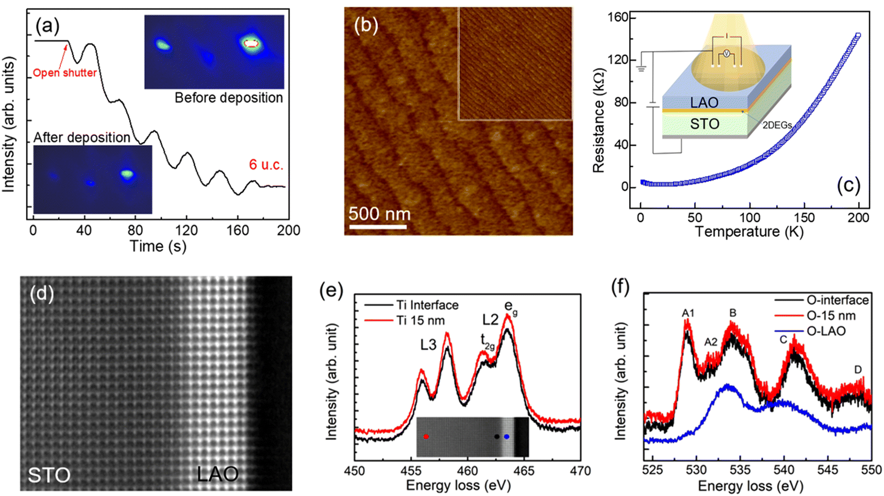 | ||
| Fig. 1 (a) RHEED oscillations during the growth of the 6 uc LAO film and RHEED diffraction patterns before (top-right inset) and after (bottom-left inset) the growth. (b) AFM images of 2 × 2 μm2 surface morphology of the LAO/STO sample, inset depicts a large view with the size of 5 × 5 μm2. (c) R–T curve of the LAO/STO heterostructure, inset schematically illustrates the structure of the prototype device. (d) STEM cross-section image of the 6 uc thick LAO/STO heterostructure. (e) Ti-L edge and (f) O-K edge electron energy-loss spectra at different regions of the LAO/STO heterostructure. The inset of (e) schematically depicts the regions where the spectra were collected. | ||
It was reported that the conducting interfacial area in LAO/STO is located ∼7 nm below the LAO layer within the STO substrate.28 Thus, HR-STEM equipped with EELS was used to study the conducting mechanism of the LAO/STO heterostructure as its spectrum-collection area is smaller than 1 nm2 and can be precisely controlled. In situ EELS were collected at the LAO layer (highlighted in blue), the interfacial area (highlighted in black), and the region 15 nm away from the interface (highlighted in red). The corresponding areas are schematically depicted in the inset of Fig. 1e. EELS provides information on both the O and Ti states from the O-K (O 1s to 2p) and Ti-L (Ti 2p to 3d) core edges, which is useful in the characterization of the oxygen vacancies in the LAO/STO 2DEG system.23,29–33 The peaks in the Ti spectrum correspond to the excitation of electrons from the inner 2p3/2 (L3 edge) and 2p1/2 levels (L2 edge) to the narrow unoccupied 3d band, resulting in two narrow peaks. They are further doubled by the crystal-field split induced by the surrounding O atoms,29 namely, the lower energy t2g and higher energy eg levels. In Fig. 1e, the Ti spectrum (highlighted in red) collected at the region located away from the interface was observed to exhibit a typical Ti spectrum in the STO layer with doubled L2 and L3 peaks.29 For the Ti spectrum (black) collected at the interfacial area, the intensity of the L2 t2g peak was observed to have weakened significantly. The weakening of the L2 t2g peak corresponds to the transfer of Ti4+ to Ti3+ for Ti ions near the interface, which was induced by the introduction of oxygen vacancies.30Fig. 1f depicts the O 1s spectrum collected in different areas, as indicated in the inset of Fig. 1e. The O spectrum (highlighted in blue) collected at the LAO layer is a typical O 1s spectrum for LAO.32 The A1 and A2 peaks correspond to the interaction of the O atom with the two nearest Ti atoms—A1 is correlated to the Ti t2g orbital and A2 is correlated to the Ti eg orbital. Compared to the Ti 2p spectrum, the difference between the spectra collected at the interface area and the region located 15 nm from the interface within STO is insignificant, except for a weak difference in the intensity. This can be attributed to two reasons. (1) There are three times as many O sites as Ti, one oxygen vacancy nominally transfers two electrons to the Ti 3d bands; consequently, a slight change in oxygen can be amplified in the Ti 2p spectrum. (2) The sample was annealed in an oxygen atmosphere (1 Torr) at 500 °C, leading to the minimization of the oxygen vacancies. Thus, it is difficult to acquire much information about the oxygen vacancies based on O 1s EELS.
Consistent with previously published works,3,21,24,34–36 oxygen vacancies were found in the interfacial region via in situ EELS analysis. Based on the EELS analysis results, we proposed a model to realize reversible metal–insulator transition (MIT) in the LAO/STO 2DEG system via electric field gating and optical illumination. As depicted in Fig. 2a, the oxygen vacancies induced defect energy levels were supposed to be slightly below the Fermi energy level and the electrons were confined to 2DEG QW. In this case, the sample exhibited a normal metallic 2DEG transport behavior. When a sufficiently large positive pulse voltage (with a 300 ms pulse width) was applied at the gate, the conduction band was bent down and the electrons escaped from 2DEG QW to the defect energy levels induced by oxygen vacancies (Fig. S2b†). This was verified to be an irreversible process by removing the applied pulse voltage.36–38 After the removal of the applied positive pulse voltage, the electrons were observed to remain in the oxygen vacancies induced defect energy levels, and the device was adjusted to an insulating state (Fig. 2b). Subsequently, optical illumination was applied to excite the electrons back to 2DEG QW; following which, the system will revert to the metallic state, as depicted in Fig. 2c. A detailed analysis of the influence of voltage gating and optical illumination was illustrated in Fig. S2 and S3.† Thus, as is shown in Fig. 2d, the reversible modulation between conducting and insulating states can be theory achieved by a combination of positive pulse voltage and optical illumination.
 | ||
| Fig. 2 Metal–insulator transition mechanism. Schematic of the LAO/STO 2DEG system and corresponding potential energy profiles for the (a) initial, (b) positive pulse voltage gating, and (c) illumination states. The arrows indicate the jumping directions of the electrons. (d) Schematic of the reversible modulation of the metal–insulator transition using the positive pulse voltage gating and illumination processes. | ||
To verify the model, electric transport properties measurements were performed under different conditions. Fig. 3a shows the R–T curves, first, the sample was cooled from 200 to 3 K using a constant gating voltage, Vg of 0, 20, 50, 80, and 130 V (gating cooling), and then, the R–T curves were measured during the warming process from 3 to 200 K without gating voltage. In the second scenario, the sample was cooled without gating, and then, a pulse gating voltage (200 V, 300 ms) was applied at 3 K. The R–T curve was also measured by warming the sample from 3 to 200 K without gating voltage. In the Vg = 0 V cooling process, the R–T curve exhibits an overall metallic behavior. The upturn at low temperatures may be related to the Kondo effect induced by the interplay between the localized Ti 3d orbital moment and unlocalized electrons.12 As Vg was increased, the resistance was observed to significantly increase over the entire temperature range. When Vg was increased above 50 V, the behavior of the R–T curves was observed to change dramatically, and the low-temperature resistance was observed to increase beyond the measurement limit of our instruments at Vg = 130 V. This observation indicates that the electrons are transferred from 2DEG QW to the defect energy levels by the gradual positive gating. It may also suggest the existence of an energy gap between the 2DEG QW and defect energy level, which blocks the transfer of free electrons between these two states. The existence of an energy gap is supported by the avalanche-like sharp drop in the resistance that was observed at 91 K in the curves corresponding to Vg = 130 V (gating cooling) and Vg = 200 V (zero-gating cooling). This avalanche-like effect is expected to be associated with thermally the assisted jumping of electrons from the defect energy levels to 2DEG QW and the decreasing dielectric constant of STO substrates with the increasing temperature (Fig. S8†). Based on the avalanche-like sharp drop at 91 K, we estimated the energy gap at 91 K to be as the thermal energy of KBT = 7.83 meV. Above 91 K, the sample was observed to recover its metallic behavior but with a much higher resistance, indicating that not all the electrons could return to the QW state due to the existence of the energy gap.
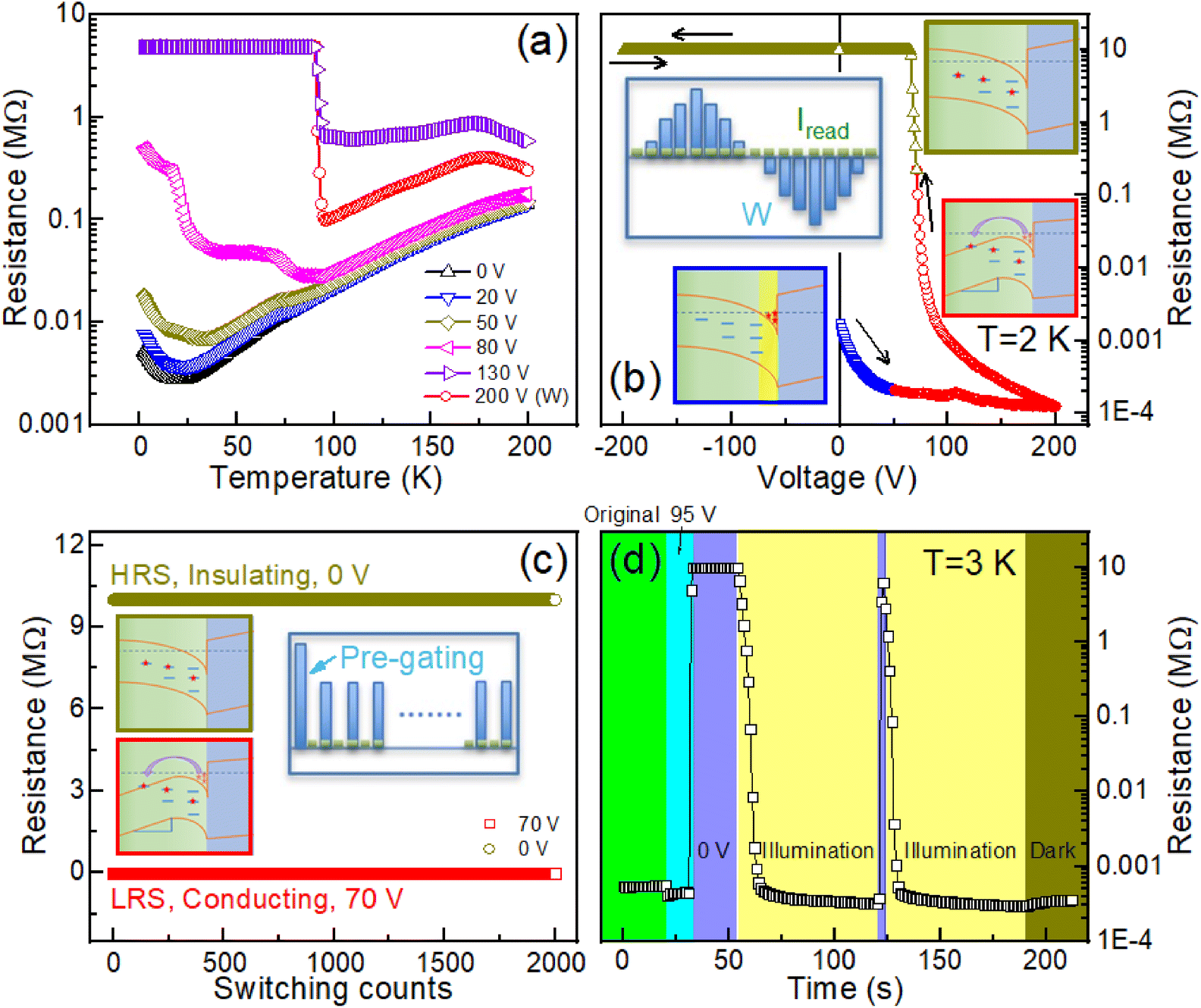 | ||
| Fig. 3 Metal–insulator transition co-modulated by voltage gating and illumination process. (a) Gating voltage-dependent R–T curves of the 2DEG system. (b) Resistance of 2DEG as a function of the gating voltage, the sample was cooled to 2 K without a pre-gating process. The corresponding band structure has been schematically depicted in the bottom-left, middle-right, and top-right insets for the Initial, ON, and OFF states, respectively. As illustrated in the top-left inset, the reading current (Iread) and write voltage (W), which follows a triangular profile, are applied simultaneously. The directions of the sweeps are indicated by arrows. (c) Reversible switching of the resistive state with the sample pre-gated by a positive voltage. The bottom-left and top-left insets depict the band structures corresponding to the ON and OFF states, respectively. The switching process is presented in the right inset. (d) Illumination and voltage gating-co-modulated metal–insulator transition at T = 3 K. | ||
To gain a deeper understanding of the gating effect on the electric transport properties of the heterostructure, the R–V curve without a pre-gating process was measured at 2 K under a constant current of 1 μA, as is shown in Fig. 3b. The dependence of R on Vg can be roughly divided into three sections: the conducting (highlighted in blue), transition (highlighted in red), and insulating sections (highlighted in dark yellow). Within the conducting section spanning 0–50 V, where the resistance was observed to decrease rapidly with increasing Vg. This was followed by the transition section at Vg ≥ 50 V, which exhibited a much slower decreasing relationship. The effect of a back-gate voltage on the LAO/STO interface was observed to be twofold. (1) It added electrons to QW when the gate voltage was increased from zero and removed electrons from QW when it was decreased. (2) It controlled the shape of the energy band of QW by tilting the conduction band profile within the STO substrate.16,37–39 As schematically depicted in the inset with a blue frame, the application of a small positive gating voltage (which was not sufficient to bend the conduction band to the defect energy level) induced electrons to be simply added to QW and allowed for a more conducting state. During the transition process, a further increase in the positive voltage caused the conduction band of the STO substrate to bend down, leading to an overlap between the conduction band and defect energy levels. This effect was observed to induce the escape of electrons from 2DEG QW to the conduction band of the STO substrate, nearly causing a saturation in resistance (as depicted in the inset with the red frame).37,39 The final process was the insulating section. When the voltage was decreased from 200 V, the resistance gradually increased and finally reached the measurement limit (10 MΩ). When the gating voltage was reverted to zero, the device attained a completely insulating state as the electrons remained at the defect energy level (the resistance of the sample was too high to be measured using a multimeter with a measurement range of 200 MΩ).
After the above-mentioned process, the sample remained insulating at a low gating voltage situation (Vg < 25 V) and became conducting at a high voltage gating situation (Vg > 25 V) (see Fig. S4a†). This suggests the possibility of resistance modulation between the high and low resistance states by varying Vg. In Fig. 3(c), the Vg of 0 V and 70 V were chosen to realize the ON (low R) and OFF (high R) states. The corresponding band structures for the ON and OFF states are shown in the bottom-left and top-left insets, respectively. To verify the reversibility of the ON/OFF states, we repeated the measurement of R at Vg = 0 and 70 V for 1000 times. The results demonstrated very good reversibility even after 1000 cycles. Further, the influence of a negative pulse voltage pre-gating process on conduction states was also investigated. Our results demonstrated that the negative pulse voltage pre-gating process does not exert significant influence on the conduction states as electrons return to 2DEG QW following the negative pulse voltage pre-gating process. Further details can be found in Fig. S5 and S6.†
Although the ON/OFF states can be achieved via a back-gate gating method, the ON state was observed to be volatile, which requires a sustainable voltage to bend the conduction band. To achieve a nonvolatile ON state, the trapped electrons need to be transmitted back to 2DEG QW. As depicted in Fig. 2c, this is achieved via the illumination method. Fig. 3d presents the influence of white light (wavelength of 400–900 nm) illumination at 3 K. The green zone illustrates the resistance of the initial metallic state, which is cooled from 300 K without a pre-gating process. Following the application of a 95 V voltage, the sample becomes more conducting (cyan zone). However, it becomes insulating when the voltage is removed (gray zone). It maintains the insulating state unless the sample is illuminated again. As is evident from the yellow region (under illumination), the resistance decreases sharply, and then, the sample transfers to a metallic state following illumination over a short period of time. During the illumination process, a 95 V voltage is applied over a duration of 1 s, and the sample is immediately tuned to an insulating state after the gating process. However, this state could be switched to the ON state using the illumination condition. Our results demonstrate that reversible modulation of the metallic and insulating states could be achieved by a combination of optical illumination and positive voltage gating processes.
To understand the physics underlying the above observations, we measure the Hall resistance at different gating voltages and temperatures (3–30 K) to gain more information about the free electrons. The samples are first cooled from room temperature to 3 K, and then, a positive pulse voltage (200 V, 300 ms) and negative pulse voltage (−40 V, 300 ms) are used to pre-gate the sample. In Fig. 4a, following the positive voltage pre-gating process, the sample becomes insulating. Thus, each of the voltage-dependent Hall resistances is measured by applying a consistent voltage capable of tuning the sample into a conducting state. A linear dependence of the Hall resistance on the applied magnetic field is observed with a negative slope, which indicates the electron-dominated conducting behavior. The voltage-dependent carrier density and electron mobility deduced from the Hall effect measurement is depicted in Fig. 4a and b, respectively. In Fig. 4a, the carrier density increases monotonically with increasing voltage, and although the mobility of electrons increases slowly from Vg = 0 to 50 V, it is observed to increase sharply and attain a maximum at Vg = 73 V. With further increase in Vg, the mobility decreases sharply and then increases to a nearly constant value at approximately Vg = 80 V. The non-monotonic behavior of electron mobility is attributed to two factors—the carrier density and trapping of electrons induced by band-bending. At low gating voltages (Vg < 50 V), which are insufficient to bend the conduction band to the defect energy level, the electrons were localized at the defect energy level, leading to a nearly zero electron mobility and an extremely slow increase in the carrier density gating voltage increasing from 50 to 73 V, the localized electrons were delocalized due to the overlap between the conduction band and the defect energy levels. The higher the gating voltage, the stronger overlap will be. Thus, both the electron mobility and carrier density were observed to increase with increasing gating voltage. However, the significantly increased electron density also induces scattering between the electrons. Thus, the electron mobility decreases with increasing gating voltage for gating voltages exceeding 73 V. In Fig. 4b, in the negative voltage case, the electrons in the 2DEG QW are gradually emptied by the negative voltage pre-gating process (Fig. S2, S5 and S6†), thus both the carrier density and mobility are observed to decrease with increasing negative voltage.
 | ||
| Fig. 4 (a) Voltage-dependent carrier density and mobility of the sample at 3 K corresponding to (a) positive voltage and (b) negative voltage. The insets depict the Hall effect data measured at different voltages. Voltage and temperature-dependent mapping of the (c) carrier density and (d) mobility of the electron. | ||
The mapping of the temperature- and voltage-dependent carrier density and electron mobility for a sample pre-gated using positive voltage (200 V) have been illustrated in Fig. 4c and d. In Fig. 4c, the high carrier density state was observed to exist within the high voltage and low temperature region. The carrier density decreased monotonically with increasing temperature and decreasing voltage. This temperature-dependent behavior was primarily dominated by the decrease in the permittivity of STO with increasing temperature (Fig. S8†).40–42 In contrast, the voltage-dependent behavior was attributed to the voltage-induced band bending.39 In Fig. 4d, the electron mobility exhibits strong temperature- and voltage-dependent behavior. In this case, the electron mobility was primarily determined by scattering. Two types of scattering were observed in the system—electron–phonon and electron–electron scattering. The former is temperature dependent, while the latter is voltage dependent. Usually, electron mobility is known to decrease with increasing temperature due to the enhancement of electron–phonon scattering. However, in this system, the mobility exhibits a mountain-like peak in the range between 73–80 V at approximately 5 K, indicating the dominance of electron–electron scattering at low temperatures. When the temperature was raised above 8 K, the mobility was primarily influenced by electron–phonon scattering. Thus, electron mobility was observed to decrease with increasing temperature.
4. Conclusions
In summary, an electrically and optically erasable non-volatile 2DEG memory was developed in this study based on LAO/STO heterostructures. High mobility electrons in the 2DEG quantum were emptied via a positive gating process, which induced an insulating state. Subsequently, the electrons were excited back to 2DEG QW via optical illumination, which caused the sample to return to a metallic state. The ON/OFF state was verified to be robust with a ratio of over 106, demonstrating the potential of applications to non-volatile memory.Author contributions
D. X. Z. and J. W. Z. contribute equally to this work. D. X. Z. and X. X. Z. designed the outline of the manuscript and wrote the main manuscript text. D. X. Z. prepared the samples and do the electric transport measurement. J. Z. performed the STEM investigation. X. H., Y. W., P. L., Y. C. W., Y. C. M., H. L. B. and H. N. A. contributed detailed discussions and revisions. All authors reviewed the manuscript.Conflicts of interest
The authors declare no competing financial interest.Acknowledgements
The research reported in this publication was supported by King Abdullah University of Science and Technology (KAUST), Office of Sponsored Research (OSR) under the Award No. OSR-2019-CRG8-4081. D. X. Z. and H. L. B. acknowledge the financial support from the National Natural Science Foundation of China (11704278, 51772207 & 11434006) and Natural Science Foundation of Tianjin City (19JCQNJC03000). We thank Dr Long Cheng for the helpful discussion at the University of Waterloo, Canada.References
- A. Ohtomo and H. Hwang, A high-mobility electron gas at the LaAlO3/SrTiO3 heterointerface, Nature, 2004, 427, 423 CrossRef CAS PubMed.
- S. Thiel, G. Hammerl, A. Schmehl, C. W. Schneider and J. Mannhart, Tunable quasi-two-dimensional electron gases in oxide heterostructures, Science, 2006, 313, 1942 CrossRef CAS PubMed.
- Y. Lei, Y. Li, Y. Z. Chen, Y. W. Xie, Y. S. Chen, S. H. Wang, J. Wang, B. G. Shen, N. Pryds, H. Y. Hwang and J. R. Sun, Visible-light-enhanced gating effect at the LaAlO3/SrTiO3 interface, Nat. Commun., 2014, 5, 5554 CrossRef CAS PubMed.
- K. A. Brown, S. He, D. J. Eichelsdoerfer, M. C. Huang, I. Levy, H. Lee, S. Ryu, P. Irvin, J. Mendez-Arroyo, C. B. Eom, C. A. Mirkin and J. Levy, Giant conductivity switching of LaAlO3/SrTiO3 heterointerfaces governed by surface protonation, Nat. Commun., 2016, 7, 10681 CrossRef CAS PubMed.
- Y. Chen, Y. Lechaux, B. Casals, B. Guillet, A. Minj, J. Gázquez, L. Méchin and G. Herranz, Photoinduced Persistent Electron Accumulation and Depletion in LaAlO3/SrTiO3 Quantum Wells, Phys. Rev. Lett., 2020, 124, 246804 CrossRef CAS PubMed.
- L. Cheng, L. M. Wei, H. X. Liang, Y. D. Yan, G. H. Cheng, M. Lv, T. Lin, T. T. Kang, G. L. Yu, J. H. Chu, Z. Y. Zhang and C. G. Zeng, Optical manipulation of Rashba spin–orbit coupling at SrTiO3-based oxide interfaces, Nano Lett., 2017, 17, 6534 CrossRef CAS PubMed.
- F. Zhang, P. Lv, Y. T. Zhang, S. J. Huang, C. M. Wong, H. M. Yau, X. X. Chen, Z. Wen, X. N. Jiang, C. G. Zeng, J. W. Hong and J. Y. Dai, Modulating the electrical transport in the two-dimensional electron gas at LaAlO3/SrTiO3 heterostructures by interfacial flexoelectricity, Phys. Rev. Lett., 2019, 122, 257601 CrossRef CAS PubMed.
- L. Guo, Y. Yan, R. Xu, J. Li and C. Zeng, Zero-Bias Conductance Peaks Effectively Tuned by Gating-Controlled Rashba Spin-Orbit Coupling, Phys. Rev. Lett., 2021, 126, 057701 CrossRef CAS PubMed.
- N. Reyren, S. Thiel, A. D. Caviglia, L. F. Kourkoutis, G. Hammerl, C. Richter, C. W. Schneider, T. Kopp, A. S. Ruetschi, D. Jaccard, M. Gabay, D. A. Muller, J. M. Triscone and J. Mannhart, Superconducting interfaces between insulating oxides, Science, 2007, 317, 1196 CrossRef CAS PubMed.
- C. Liu, X. Yan, D. Jin, Y. Ma, H. W. Hsiao, Y. Lin, T. M. Bretz-Sullivan, X. Zhou, J. Pearson, B. Fisher and J. S. Jiang, Two-dimensional superconductivity and anisotropic transport at KTaO3 (111) interfaces, Science, 2021, 371, 716–721 CrossRef CAS PubMed.
- Z. Chen, Y. Liu, H. Zhang, Z. Liu, H. Tian, Y. Sun, M. Zhang, Y. Zhou, J. R. Sun and Y. W. Xie, Electric field control of superconductivity at the LaAlO3/KTaO3 (111) interface, Science, 2021, 372, 721–724 CrossRef CAS PubMed.
- A. Brinkman, M. Huijben, M. Van Zalk, J. Huijben, U. Zeitler, J. C. Maan, W. G. Van der Wiel, G. Rijnders, D. H. A. Blank and H. Hilgenkamp, Magnetic effects at the interface between non-magnetic oxides, Nat. Mater., 2007, 6, 493 CrossRef CAS PubMed.
- E. Lesne, Y. Fu, S. Oyarzun, J. C. Rojas-Sanchez, D. C. Vaz, H. Naganuma, G. Sicoli, J. P. Attane, M. Jamet, E. Jacquet, J. M. George, A. Barthelemy, H. Jaffres, A. Fert, M. Bibes and L. Vila, Highly efficient and tunable spin-to-charge conversion through Rashba coupling at oxide interfaces, Nat. Mater., 2016, 15, 1261 CrossRef CAS PubMed.
- Q. Song, H. R. Zhang, T. Su, W. Yuan, Y. Y. Chen, W. Y. Xing, J. Shi, J. R. Sun and W. Han, Observation of inverse Edelstein effect in Rashba-split 2DEG between SrTiO3 and LaAlO3 at room temperature, Sci. Adv., 2017, 3, e1602312 CrossRef PubMed.
- A. D. Caviglia, S. Gariglio, N. Reyren, D. Jaccard, T. Schneider, M. Gabay, S. Thiel, G. Hammerl, J. Mannhart and J. M. Triscone, Electric field control of the LaAlO3/SrTiO3 interface ground state, Nature, 2008, 456, 624 CrossRef CAS PubMed.
- C. Bell, S. Harashima, Y. Kozuka, M. Kim, B. G. Kim, Y. Hikita and H. Y. Hwang, Dominant mobility modulation by the electric field effect at the LaAlO3/SrTiO3 interface, Phys. Rev. Lett., 2009, 103, 226802 CrossRef CAS PubMed.
- A. D. Caviglia, M. Gabay, S. Gariglio, N. Reyren, C. Cancellieri and J. M. Triscone, Tunable Rashba spin-orbit interaction at oxide interfaces, Phys. Rev. Lett., 2010, 104, 126803 CrossRef CAS PubMed.
- Y. W. Xie, Y. Hikita, C. Bell and H. Y. Hwang, Control of electronic conduction at an oxide heterointerface using surface polar adsorbates, Nat. Commun., 2011, 2, 494 CrossRef PubMed.
- D. A. Dikin, M. Mehta, C. W. Bark, C. M. Folkman, C. B. Eom and V. Chandrasekhar, High Electron Mobility, Coexistence of superconductivity and ferromagnetism in two dimensions, Phys. Rev. Lett., 2011, 107, 056802 CrossRef CAS PubMed.
- N. Nakagawa, H. Y. Hwang and D. A. Muller, Why some interfaces cannot be sharp, Nat. Mater., 2006, 5, 204 CrossRef CAS.
- G. Herranz, M. Basletic, M. Bibes, C. Carretero, E. Tafra, E. Jacquet, K. Bouzehouane, C. Deranlot, A. Hamzic, J. M. Broto, A. Barthelemy and A. Fert, High mobility in LaAlO3/SrTiO3 heterostructures: origin, dimensionality, and perspectives, Phys. Rev. Lett., 2007, 98, 216803 CrossRef CAS PubMed.
- Z. Q. Liu, C. J. Li, W. M. Lu, X. H. Huang, Z. Huang, S. W. Zeng, X. P. Qiu, L. S. Huang, A. Annadi, J. S. Chen, J. M. D. Coey, T. Venkatesan and Ariando, Origin of the two-dimensional electron gas at LaAlO3/SrTiO3 interfaces: the role of oxygen vacancies and electronic reconstruction, Phys. Rev. X, 2013, 3, 021010 CAS.
- M. Sing, G. Berner, K. Goss, A. Muller, A. Ruff, A. Wetscherek, S. Thiel, J. Mannhart, S. A. Pauli, C. W. Schneider, P. R. Willmott, M. Gorgoi, F. Schafers and R. Claessen, Profiling the interface electron gas of LaAlO3/SrTiO3 heterostructures with hard X-ray photoelectron spectroscopy, Phys. Rev. Lett., 2009, 102, 176805 CrossRef CAS PubMed.
- W. Siemons, G. Koster, H. Yamamoto, W. A. Harrison, G. Lucovsky, T. H. Geballe, D. H. A. Blank and M. R. Beasley, Origin of charge density at LaAlO3 on SrTiO3 heterointerfaces: Possibility of intrinsic doping, Phys. Rev. Lett., 2007, 98, 196802 CrossRef PubMed.
- M. Huijben, G. Rijnders, D. H. A. Blank, S. Bals, S. Van Aert, J. Verbeeck, G. Van Tendeloo, A. Brinkman and H. Hilgenkamp, Electronically coupled complementary interfaces between perovskite band insulators, Nat. Mater., 2006, 5, 556 CrossRef CAS PubMed.
- J. N. Eckstein, Watch out for the lack of oxygen, Nat. Mater., 2007, 6, 473 CrossRef CAS PubMed.
- V. T. Tra, J. W. Chen, P. C. Huang, B. C. Huang, Y. Cao, C. H. Yeh, H. J. Liu, E. A. Eliseev, A. N. Morozovska, J. Y. Lin, Y. C. Chen, M. W. Chu, P. W. Chiu, Y. P. Chiu, L. Q. Chen, C. L. Wu and Y. H. Chu, Ferroelectric control of the conduction at the LaAlO3/SrTiO3 heterointerface, Adv. Mater., 2013, 25, 3357 CrossRef CAS PubMed.
- M. Basletic, J. L. Maurice, C. Carretero, G. Herranz, O. Copie, M. Bibes, E. Jacquet, K. Bouzehouane, S. Fusil and A. Barthelemy, Mapping the spatial distribution of charge carriers in LaAlO3/SrTiO3 heterostructures, Nat. Mater., 2008, 7, 621 CrossRef CAS PubMed.
- Z. L. Zhang, W. Sigle and M. Ruhle, Atomic and electronic characterization of the a [100] dislocation core in SrTiO3, Phys. Rev. B: Condens. Matter Mater. Phys., 2002, 66, 094108 CrossRef.
- D. A. Muller, N. Nakagawa, A. Ohtomo, J. L. Grazul and H. Y. Hwang, Atomic-scale imaging of nanoengineered oxygen vacancy profiles in SrTiO3, Nature, 2004, 430, 657 CrossRef CAS PubMed.
- L. F. Kourkoutis, H. L. Xin, T. Higuchi, Y. Hotta, J. H. Lee, Y. Hikita, D. G. Schlom, H. Y. Hwang and D. A. Muller, Atomic-resolution spectroscopic imaging of oxide interfaces, Philos. Mag., 2010, 90, 4731 CrossRef CAS.
- G. Drera, G. Salvinelli, A. Brinkman, M. Huijben, G. Koster, H. Hilgenkamp, G. Rijnders, D. Visentin and L. Sangaletti, Band offsets and density of Ti3+ states probed by X-ray photoemission on LaAlO3/SrTiO3 heterointerfaces and their LaAlO3 and SrTiO3 bulk precursors, Phys. Rev. B: Condens. Matter Mater. Phys., 2013, 87, 075435 CrossRef.
- H. Zaid, M. H. Berger, D. Jalabert, M. Walls, R. Akrobetu, I. Fongkaew and A. Sehirlioglu, Atomic-resolved depth profile of strain and cation intermixing around LaAlO3/SrTiO3 interfaces, Adv. Mater., 2020, 32, 1908242 CrossRef PubMed.
- A. Kalabukhov, R. Gunnarsson, J. Borjesson, E. Olsson, T. Claeson and D. Winkler, Effect of oxygen vacancies in the SrTiO3 substrate on the electrical properties of the LaAlO3/SrTiO3 interface, Phys. Rev. B: Condens. Matter Mater. Phys., 2007, 75, 121404 CrossRef.
- Z. Q. Liu, D. P. Leusink, X. Wang, W. M. Lu, K. Gopinadhan, A. Annadi, Y. L. Zhao, X. H. Huang, S. W. Zeng, Z. Huang, A. Srivastava, S. Dhar, T. Venkatesan and Ariando, Metal-Insulator Transition in SrTiO3−x Thin Films Induced by Frozen-Out Carriers, Phys. Rev. Lett., 2011, 107, 146802 CrossRef CAS PubMed.
- C. H. Yin, A. E. M. Smink, I. Leermakers, L. M. K. Tang, N. Lebedev, U. Zeitler, W. G. van der Wiel, H. Hilgenkamp and J. Aarts, Electron Trapping Mechanism in LaAlO3/SrTiO3 Heterostructures, Phys. Rev. Lett., 2020, 124, 017702 CrossRef CAS PubMed.
- J. Biscaras, S. Hurand, C. Feuillet-Palma, A. Rastogi, R. C. Budhani, N. Reyren, E. Lesne, J. Lesueur and N. Bergeal, Limit of the electrostatic doping in two-dimensional electron gases of LaXO3 (X = Al, Ti)/SrTiO3, Sci. Rep., 2014, 4, 6788 CrossRef CAS PubMed.
- M. S. Safeen, M. Can, A. Khare, E. D. Gennaro, A. Sambri, A. Leo, N. Scopigno, U. S. Uccio and F. M. Granozio, Non-volatile, reversible metal-insulator transition in oxide interfaces controlled by gate voltage and light, 2017, https://arxiv.org/pdf/1701.03660.pdf.
- K. Hirakawa, H. Sakaki and J. Yoshino, Mobility modulation of the two-dimensional electron gas via controlled deformation of the electron wave function in selectively doped AlGaAs-GaAs heterojunctions, Phys. Rev. Lett., 1985, 54, 1279 CrossRef CAS PubMed.
- J. Park, B. G. Cho, K. D. Kim, J. Koo, H. Jang, K. T. Ko, J. H. Park, K. B. Lee, J. Y. Kim, D. R. Lee, C. A. Burns, S. S. A. Seo and H. N. Lee, Oxygen-vacancy-induced orbital reconstruction of Ti ions at the interface of LaAlO3/SrTiO3 heterostructures: A resonant soft-X-ray scattering study, Phys. Rev. Lett., 2013, 110, 017401 CrossRef CAS PubMed.
- O. Okhay, A. Tkach, A. Wu and P. M. Vilarinho, Manipulation of dielectric permittivity of sol–gel SrTiO3 films by deposition conditions, J. Phys. D: Appl. Phys., 2013, 46, 505315 CrossRef.
- K. A. Müller and H. Burkard, An intrinsic quantum paraelectric below 4 K, Phys. Rev. B: Condens. Matter Mater. Phys., 1979, 19, 3593 CrossRef.
Footnote |
| † Electronic supplementary information (ESI) available: Method, temperature dependence of resistance, metal–insulator transition mechanism. Temperature dependent R–V curves, R–V curves, reversible switching, temperature dependent dielectric constant, effect of illumination, time dependence of resistance. See DOI: https://doi.org/10.1039/d2nr01582j |
| This journal is © The Royal Society of Chemistry 2022 |