DOI:
10.1039/D2NR00818A
(Paper)
Nanoscale, 2022,
14, 8463-8473
Prediction of 2D IV–VI semiconductors: auxetic materials with direct bandgap and strong optical absorption†
Received
11th February 2022
, Accepted 7th May 2022
First published on 20th May 2022
Abstract
Auxetic materials are highly desirable for advanced applications because of their negative Poisson's ratios, which are rather scarce in two-dimensional materials. Motivated by the elemental mutation method, we predict a new class of monolayer IV–VI semiconductors, namely, δ-IV–VI monolayers (GeS, GeSe, SiS and SiSe). Distinctly different from the previously predicted IV–VI monolayers, the newly predicted δ-MX (X = Ge and Si; M = S and Se) monolayers exhibit a puckered unit cell with a space group of Pca21. Their stabilities were confirmed by first-principles lattice dynamics and molecular dynamics calculations. In particular, all these MX monolayers possess a large bandgap in the range of 2.08–2.65 eV and pronounced anisotropic mechanical properties, which are demonstrated by direction-dependent in-plane Young's moduli and Poisson's ratios. Furthermore, all these 2D MX monolayers possess negative Poisson's ratios (even up to about −0.3 for SiSe). Strong optical absorption is observed in these δ-IV–VI monolayers. These interesting physical properties will stimulate the development of 2D flexible devices based on IV–VI semiconductor monolayers.
1. Introduction
Graphenes are considered as the horizon of two-dimensional (2D) materials, as they inspire intense research activity on 2D layered materials,1,2 which have fantastic mechanical,3–5 electronic,6 thermal7–10 and magnetic11 properties. The Dirac cone in graphenes induces ultrafast dynamics for the charge carrier, but their zero bandgap characteristics also impede some applications in field-effect transistors, impelling the further investigation of other 2D semiconductor materials.12 Black phosphorus (BP) is an ideal alternative for 2D electronics because of its high charge carrier mobility and high on–off ratio in field-effect transistor application. Duo to the puckered honeycomb structure, the physical properties of BP exhibit pronounced anisotropy. For example, the thermal conductivity of BP is about 20 and 40 W m−1 K−1 along armchair and zigzag directions with a thickness of 15 nm, which can be further decreased by reducing the thickness,13 mainly contributed by strong anisotropy in phonon group velocities.14 Furthermore, the BP-based nanophononic heterostructure shows novel thermal management ability with tunable interfacial thermal resistance.15 The electronic band structure of 2D semiconductors can be further tuned,16,17 which opens prospects for the design of various innovative devices for applications in flexible electronics, spintronics, photocatalysis, and artificial synapses.18–22 Inspired by the successful demonstration of these 2D materials, extensive effort has been conducted to expand the family of 2D materials.23,24 Since the synthesis of new 2D materials is time-consuming and costly, the theoretical calculation is of great utility. Some new 2D materials such as 2D magnetic MSi2CxN4−x (M = Cr, Mo, and W; x = 1 and 2),25 anisotropic MBs (M = Cr, Mn or Fe; B = boron),26 CrX3 (X = I, Br, and Cl),27 tetragonal and hexagonal boron nitride,28 graphene-like Si1−xGex,29 α′-boron sheet,30 and B2X3 (X = Se and Te) photocatalysts31 are theoretically predicted by different theoretical schemes, which present a set of unique functional properties.32–34
Recently, auxetic materials characterized by negative Poisson's ratios (NPRs) have attracted tremendous research attention from both fundamental science and practical application points of view.35–37 Poisson's ratio is defined as the ratio of the lateral contraction strain to the longitudinal extension strain. Negative Poisson's ratio reveals that the material would expand laterally when stretched longitudinally. This is totally opposite to most of the conventional materials, which tend to shrink laterally when subjected to strain in the longitudinal direction.38 Bulk auxetic materials have been studied for some applications. For example, a NPR copper foam was synthesized experimentally, which displays enhanced toughness.39 To explore the effect of the chondrocyte proliferation on the cartilage regeneration by a compress, polyurethane materials with NPRs were used for such tissue engineering.40 The NPR fastener was designed using ceramic aerogels via 3D graphene structures, which possesses novel mechanical properties.41 For metals, a correlation between the NPR and work function was demonstrated based on the electron-gas model, which enables a promising application in highly sensitive detectors because negative Poisson's ratios of the metal electrodes can amplify the response of strain on sensor sheets.42 A hierarchical tube was proposed with a NPR characteristic that it will extend along the transverse direction by the vertical force as harder composites.43 Some other studies also demonstrated that bulk materials with NPRs have fantastic properties for a muffler and a shock absorber.44,45
In particular, nanomaterials with NPRs have more advantages because of their particular unique structure,46–48 which also inspired tremendous prediction from both theoretical and computational efforts.49 The puckered structure in BP has proven to induce anisotropic characteristics and a NPR in the out-of-plane direction,50 which is also demonstrated in the experiment.51 Besides, δ-phosphorene has a remarkable NPR (−0.267) along the grooved direction, excellent flexibility and critical crack strain showing a potential usage for electromechanical devices.52 B4N monolayers were predicted to have dynamic and thermal stabilities and excellent mechanical properties with a maximal NPR of −0.032, which can be considered as future nanomechanical devices.53 GaPS4 monolayers were reported to exhibit a NPR of −0.033 in the in-plane and −0.62 in the out-of-plane direction. Combined with its ultralow cleavage energy (about 0.23 J m−2), 2D GaPS4 is expected to be a promising candidate for nanoelectronics and electromechanical devices.54 The NPR characteristic in 2D blue phosphorus oxide was also reported, and the mechanism is attributed to the competition between attractive P–P bonding and repulsive P–O bonding, respectively.55 For other 2D NPR materials, orbital coupling and hybridization of the electron are also possible origin of negative Poisson's ratios.56,57 It is worth noting that auxetic materials are especially appropriate in the application of flexible or bio-electronics. Because most biological materials have a negative Poisson ratio, in such applications, the substrate made of non-auxetic materials may result in a mismatch in deformation and cause irritation.58
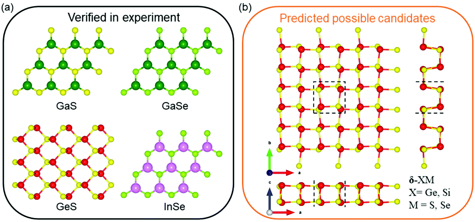
Very recently, IV–VI-based monolayers59,60 such as GaS,61 GaSe,62 GeS63,64 and InSe65 monolayers have aroused tremendous attention, shown as Fig. 1(a), which were synthetized in the experiment as high-performance photodetectors. In detail, the IV–VI compounds have been proposed with different structures such as the monolayer Pcnm-GeSe, Pmma-SiS and Pma2-SiS.66,67 The SiSe monolayer was also predicted to have Pmma and Pma2 structures.68,69 Puckered SiS and SiSe were suggested in previous reports.70,71 In this work, we predict a family of 2D group δ-IV–IV monochalcogenide materials, XM (X = Ge and Si; M = S and Se), using the first-principles calculation and ab initio molecular dynamics (AIMD) method. The XM monolayers possess pronounced direction-dependent NPR characteristics. Besides, the electronic band structure and direction-dependent Young's modulus are discussed. The ultra-strong optical absorption property of those layered materials is characterized as well. These multi-functional features support promising applications in nanoelectronics, nanomechanical and optoelectronic devices.
 |
| | Fig. 1 (a) Synthesized IV–VI monolayers in a previous experiment and (b) crystal structure of the newly predicted δ-IV–VI monolayers XM (X = Ge and Si; M = S and Se). The yellow and red balls are M and X atoms, respectively. | |
2. Computational methodology
Based on density functional theory (DFT), the first-principles method was explored using the Vienna Ab initio Simulation Package (VASP)72 with the projector-augmented wave method. The Perdew–Burke–Ernzerhof functional was adopted. Besides, the hybrid Heyd–Scuseria–Ernzerhof (HSE06) functional was considered by the standard screening and the standard mixing parameter of 0.2 Å−1 and 0.25, respectively.73 The cutoff energy was set at 500 eV for plane-wave, and the k-mesh was demonstrated by 8 × 8 × 1. The Brillouin zone was explored with the convergence criteria of the energy by 10−8 eV and force by 10−4 eV Å−1 in a vacuum layer thickness of about 20 Å. The minimum energy pathways of different phase transitions were determined by a climbing image nudged elastic band method (NEB)74 based on the interatomic forces and total energies acquired from the DFT calculations. The Brillouin zone (BZ) was sampled by the gamma method with 7 × 7 × 1 k-point sampling; meanwhile, the criteria for energy convergence and force convergence are 10−6 eV per cell and 0.01 eV Å−1, respectively. Furthermore, the density functional perturbation theory calculation was conducted to investigate the phonon dispersion of the materials, which was realized using the PHONOPY package.75,76
3. Results and discussion
3.1 Structure and stability
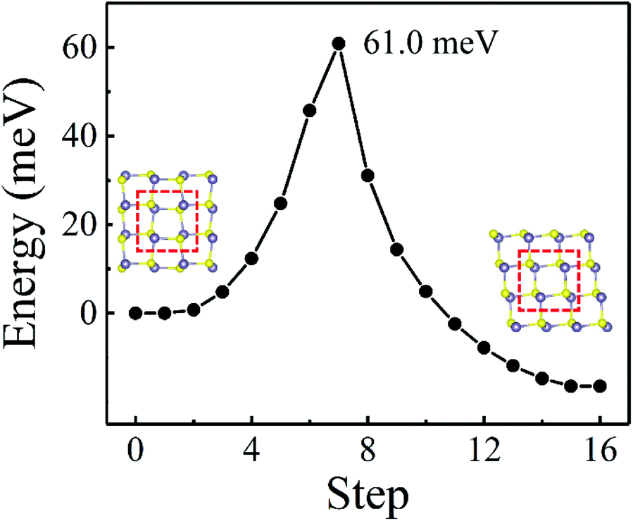
The anisotropic crystal structure of the XM (X = Ge and Si; M = S and Se) monolayers is presented in Fig. 1(b), which shows a puckered unit cell with a space group of Pca21, constructed by elemental mutation based on the prototype of δ-CS structures,77 different from the well-known orthorhombic layered structure with space group Pcmn of GeS and GeSe.66,78 The optimized unit cell of the XM monolayer contains 4 X and 4 M atoms and the obtained lattice constants, a (or b), of the GeS, GeSe, SiS and SiSe monolayers are 5.58, 5.83, 5.50 and 5.69 Å (5.76, 5.81, 5.67 and 5.73 Å), respectively. The cohesive energy of the XM system was calculated using (4EX + 4EM − EXM)/8, where EX, EM and EXM are the total energies of a X atom, a M atom and the XM, respectively. The cohesive energies of the monolayer GeS, GeSe, SiS and SiSe are 3.61, 3.37, 3.81, 3.51 eV per atom (as shown in Table 1), respectively, which are comparable with that of germanene (about 3.24 eV per atom), phosphorene (about 3.48 eV per atom) and silicene (about 3.91 eV per atom).79 Furthermore, the obtained cohesive energy of SiS is larger than that of puckered SiS (3.16 eV per atom),80 and the calculated cohesive energy of GeS and GeSe monolayers in our work is also similar to some reported GeS, GeSe with other phases, as presented in Table 2. The predicted new IV–VI monolayers can be synthesized in the experiment by a chemical vapour deposition method, and then be isolated by mechanical, sonicated or liquid-phase exfoliation, which have been adopted to synthesize few-layer GaSe62 and GeS.64 In addition, the δ-IV–IV monolayers can also be obtained by shifting X atoms in puckered IV–IV monolayer structures.81 Furthermore, the X–M bond lengths in the GeS, GeSe, SiS and SiSe monolayers are 2.42, 2.54, 2.32 and 2.44 Å, respectively. We also take GeS as an example to estimate the stability by the structural transition barrier between δ-GeS and α-GeS in Table 2. The NEB calculated energy barrier is about 61.0 meV, which is far higher than the thermal kinetic energy of about 13 meV at room temperature (1/2kBT, T = 300 K), avoiding such structural transformation, as shown in Fig. 2.
 |
| | Fig. 2 Structural transition barrier between δ-GeS and α-GeS obtained by NEB calculations. | |
Table 1 Cohesive energy (E, eV), ratio of lattice constants (b/a) along different directions, bandgap (Eg, eV) and elastic constants (N m−1) of the monolayer XM system
| |
E
|
b/a |
C
11
|
C
22
|
C
12
|
C
66
|
E
PBEg
|
E
HSEg
|
| GeS |
3.61 |
1.01 |
41.21 |
22.83 |
−4.38 |
7.64 |
1.920 |
2.65 |
| GeSe |
3.37 |
1.01 |
42.79 |
32.56 |
−7.51 |
7.41 |
1.60 |
2.20 |
| SiS |
3.81 |
1.03 |
50.29 |
24.75 |
−4.10 |
7.67 |
1.42 |
2.15 |
| SiSe |
3.51 |
1.01 |
50.35 |
33.68 |
−9.78 |
7.77 |
1.46 |
2.08 |
Table 2 Symmetry groups, cohesive energy (E, in eV) and bandgap (Eg, HSE, in eV) of the investigated GeS and GeSe monolayers in this work compared with the previous structures
| |
Space group |
E
|
E
g
|
Ref. |
| δ-GeS |
Pca21 |
3.61 |
2.65 |
This work |
| δ-GeSe |
Pca21 |
3.37 |
2.20 |
This work |
| α-GeS |
Pmn21 |
3.76 |
1.72 |
82–84
|
| β-GeS |
P3m1 |
3.74 |
2.47 |
83 and 85 |
| γ-GeS |
Pmn21 |
3.74 |
1.77 |
83 and 86 |
| α-GeSe |
Pmn21 |
3.88 |
1.75 |
87 and 88 |
| β-GeSe |
P3m1 |
3.85 |
3.01 |
85 and 88 |
| γ-GeSe |
Pmn21 |
3.83 |
2.53 |
59 and 88 |
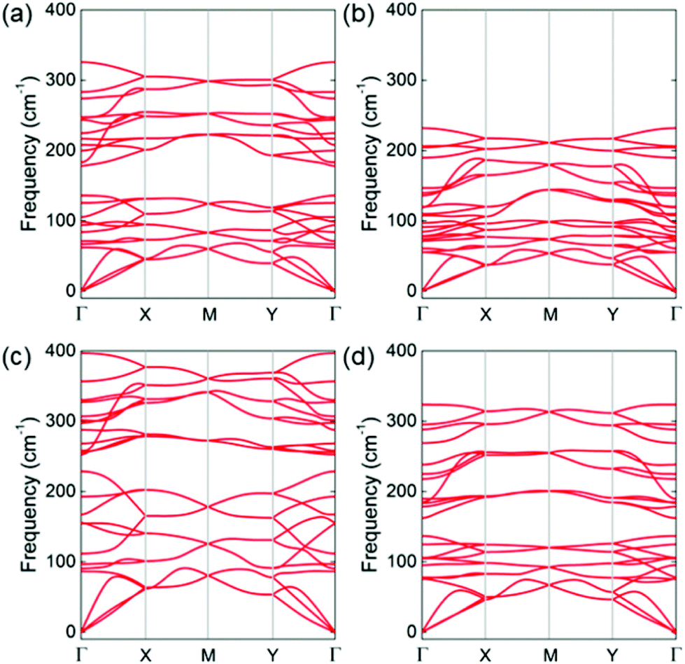
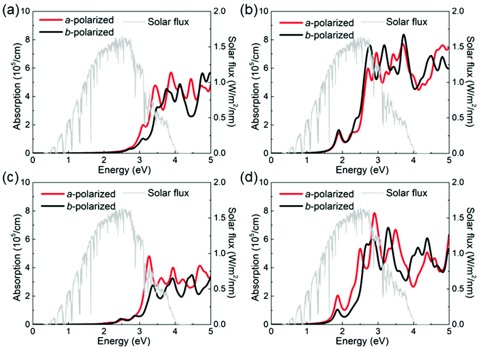
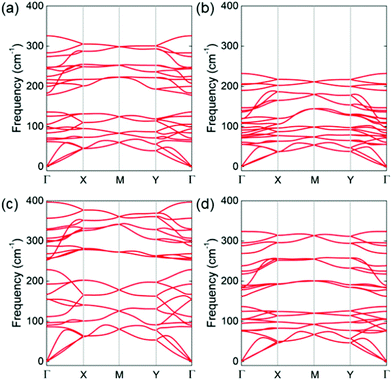
The phonon dispersion of the GeS, GeSe, SiS and SiSe monolayers was calculated, as shown in Fig. 3, characterized by 3 acoustic branches and 21 optical branches. Importantly, no imaginary frequency is found in these phonon dispersions showing a dynamic stability of these newly predicted XM monolayers. Besides, the maximum frequencies of the phonon dispersion for the GeS, GeSe, SiS and SiSe monolayers are 325, 232, 397 and 324 cm−1, respectively. Furthermore, the AIMD calculation was employed to explore the thermal stability of those layered materials using a Nosé–Hoover heat bath scheme.89 Taking the lattice translational constraints into consideration, the unit cell of the XM monolayer was expanded by an 8 × 8 × 1 supercell, which includes 128 atoms within the AIMD simulation. After a relaxation time of 5 ps, the structures of GeS, GeSe, SiS and SiSe monolayers were still undamaged at an ambient temperature of 300 K, as shown in the inset in Fig. 4(a)–(d), respectively. The temperature and total energy fluctuations versus simulation time are also presented in Fig. 4, which exhibits a convergence for the AIMD results.
 |
| | Fig. 3 Phonon dispersion of the (a) GeS, (b) GeSe, (c) SiS and (d) SiSe monolayers, respectively. | |
 |
| | Fig. 4 Total energy and the temperature fluctuation of the (a) GeS, (b) GeSe, (c) SiS and (d) SiSe monolayers during the AIMD simulation, the insets are the atomic structure after 5 ps at 300 K. The red, yellow, cyan and blue marks represent the Ge, S, Se and Si atoms, respectively; the red and gray lines represent the system total energy and temperature calculated by the AIMD simulation. | |
3.2 Electronic and mechanical properties
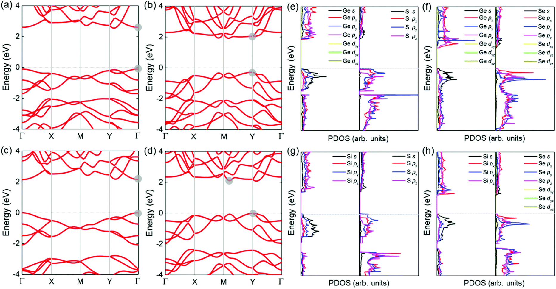
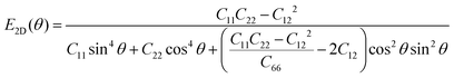
The HSE06 functional was used to calculate the band structure of the GeS, GeSe, SiS and SiSe monolayers, as shown in Fig. 5(a)–(d), respectively. It is worth noting that all those 2D materials are semiconductors. In detail, the GeS monolayer has a direct band structure with a bandgap of 2.65 eV, and the valence band maximum (VBM) and conduction band minimum (CBM) are at Γ point. In contrast, the GeS monolayer with a honeycomb hexagonal structure is an indirect bandgap semiconductor, with a bandgap of 2.47 eV.83 The band structure of GeSe and SiS monolayers have an almost direct bandgap (2.20 eV and 2.15 eV) with the CBM and VBM located near the Y (GeSe) point and Γ (SiS) point, respectively. While the GeSe monolayer with a hexagonal structure possesses an indirect bandgap (bandgap of 2.92 eV obtained by HSE06 calculation).90 The bandgaps of the IV–VI monolayer with different structures are summarized in Table 2. In contrast, the SiSe monolayer exhibits an indirect bandgap with VBM at the Y point, while the CBM is on the M–Y path. The PBE calculated density of states of the GeS, GeSe, SiS and SiSe monolayers is presented in Fig. 5(e)–(h), respectively. It is clear that the CBM and VBM of the GeS are mainly contributed from Ge_px, Ge_py and Ge_s, S_py, respectively. While the CBM and VBM of the GeSe are mainly contributed by Ge_py and Ge_s, S_px, respectively. Similar orbital contribution is also observed in the partial density of states (PDOS) of the SiS and SiSe monolayers.
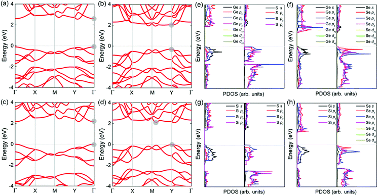 |
| | Fig. 5 Band structure of the monolayer (a) GeS, (b) GeSe, (c) SiS and (d) SiSe calculated by the HSE06 method, and the partial density of states of the monolayer (e) GeS, (f) GeSe, (g) SiS and (h) SiSe calculated by PBE. In (a–d), the locations of the CBM and VBM are marked by grey dots. | |
Next, the orientation dependence of in-plane Young's moduli and Poisson's ratios for those four layered materials were calculated as follows:53
| |  | (1) |
| |  | (2) |
where
E2D(
θ) and
v(
θ) are Young's moduli and Poisson's ratios, respectively; the angle
θ is between the considered direction and
a-direction.
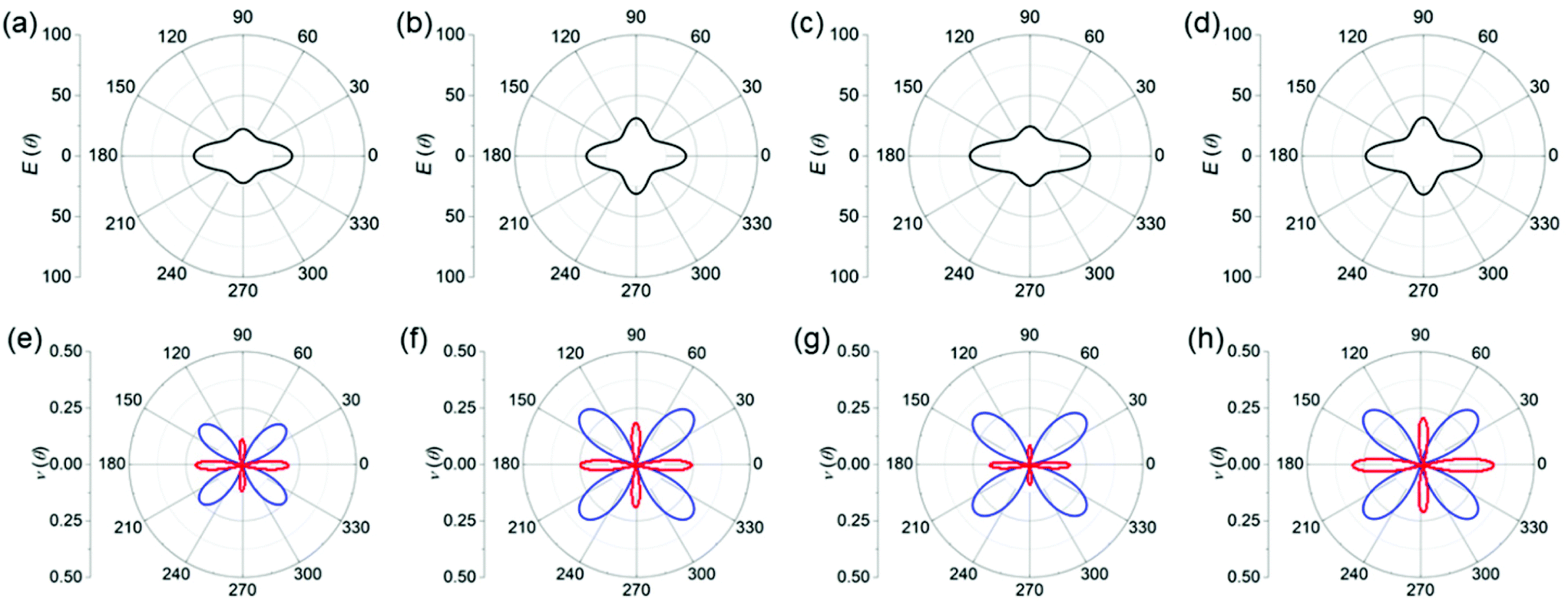
Fig. 6(a)–(d) show direction-dependent Young's moduli of the GeS, GeSe, SiS and SiSe monolayers. Obviously, these monolayer materials are anisotropy with maximal Young's moduli located at
θ = 0° with 40, 41, 50 and 47 N m
−1, respectively, while minimal Young's moduli are 19, 20, 20 and 21 N m
−1, respectively, at
θ values of about 51°, 46°, 47° and 45°. In the
b-direction, Young's moduli of the GeS, GeSe, SiS and SiSe monolayers were calculated to be 22, 31, 24 and 32 N m
−1, respectively. However, such anisotropic characteristic of Young's moduli does not exist in the honeycomb hexagonal IV–VI monolayer.
83 Furthermore, Poisson's ratios (as shown in
Fig. 6(e)–(h)) also reveal remarkable direction dependence. The GeS, GeSe, SiS and SiSe monolayers possess a maximal Poisson ratio of about 0.248, 0.333, 0.320 and 0.331 along the 45° direction, respectively. The calculated NPRs of the GeS, GeSe, SiS and SiSe monolayers along the
a-direction are −0.192, −0.231, −0.165 and −0.290, respectively, and the obtained NPRs along
b-direction are −0.106, −0.176, −0.081 and −0.194. It should be noted that the GeSe and SiSe monolayers possess pronounced NPR characteristics, which are larger than other reported 2D materials such as δ-phosphorene (−0.267),
52 PtI
2 (−0.24),
91 and Ag
2S (−0.12).
92 It is worth noting that the puckered IV–VI monolayers were also reported to possess NPRs such as GeS (−0.208), GeSe (−0.433)
93 and
Pma2-SiS monolayers (−0.19).
68 In particular, the puckered SiS has a maximal in-plane Poisson ratio of 1.025,
94 which is larger than that of SiS (0.320) reported in this work. The maximal in-plane Poisson ratio for puckered SiSe is 0.330,
94 almost the same as the Poisson ratio of the SiSe structure (0.331) in this work. Interestingly, the puckered SiS and SiSe monolayers possess out-of-plane Poisson's ratios of −0.073 and −0.466, respectively.
94
 |
| | Fig. 6 Young's modulus of the (a) GeS, (b) GeSe, (c) SiS and (d) SiSe monolayers; the Poisson ratios of the (e) GeS, (f) GeSe, (g) SiS and (h) SiSe monolayers, respectively. The blue and red lines represent the positive and negative values. | |
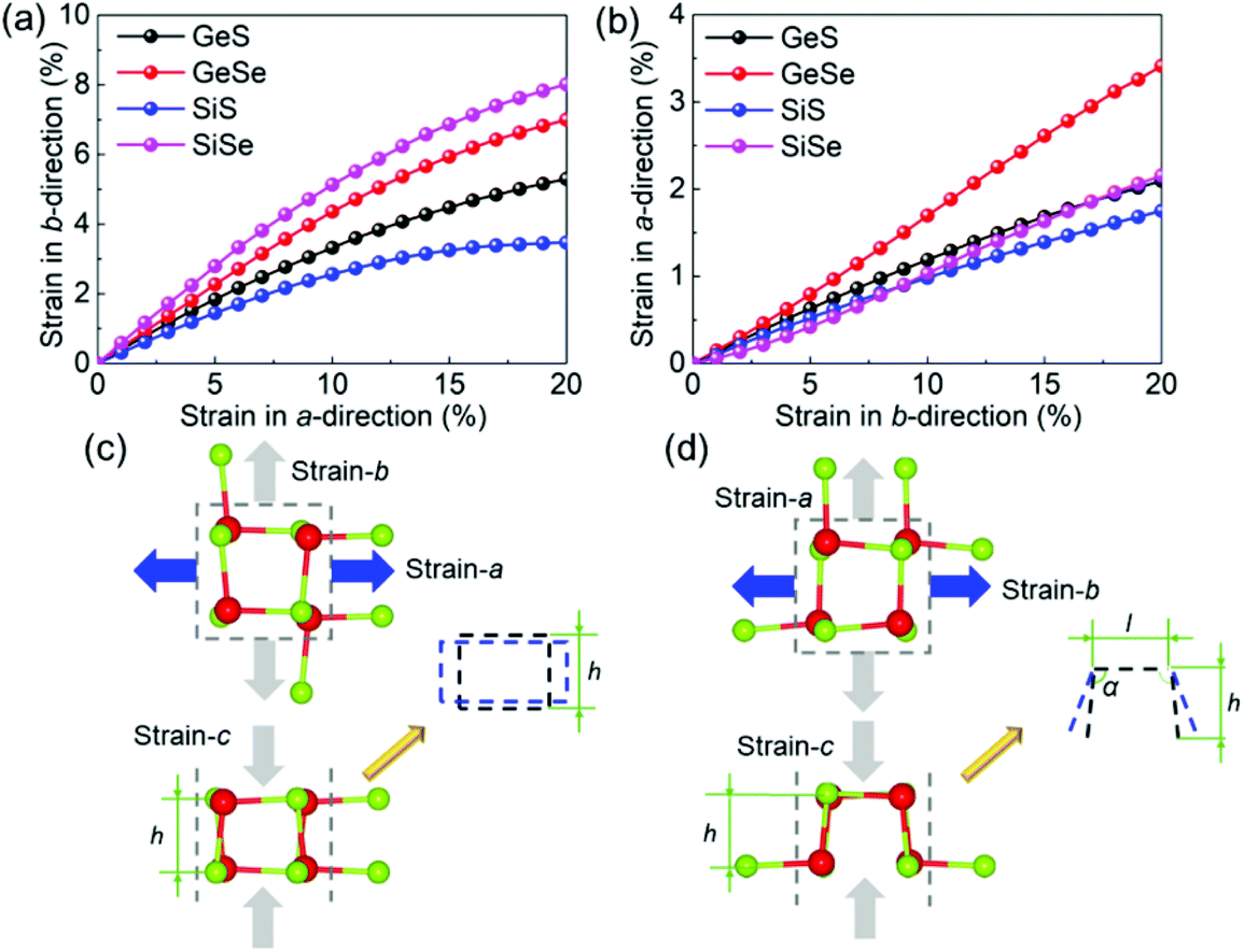
In addition, the strain in the b-direction was calculated under different uniaxial a-direction strains, as shown in Fig. 7(a), which further prove the auxetic characteristic of 2D GeS, GeSe, SiS and SiSe monolayers. Meanwhile, by fitting the results, the obtained Poisson ratios of the GeS, GeSe, SiS and SiSe monolayers are −0.193, −0.264, −0.184 and −0.294, respectively, which are comparable with the results from eqn (2). Similarly, the fitted Poisson ratios of the GeS, GeSe, SiS and SiSe monolayers in the b-direction are −0.108, −0.181, −0.089 and −0.121, respectively, as shown in Fig. 7(b).
 |
| | Fig. 7 (a) Strain in the b-direction under the external uniaxial a-direction strain and (b) the strain in the a-direction under the external uniaxial b-direction strain of the GeS, GeSe, SiS and SiSe monolayers; the schematic diagram of thickness deformation by the strain along the (c) a-direction and (d) b-direction of the MX monolayers; here the loading strain is shown in blue, while the induced strain is shown in grey. | |
When the tensile stress is applied along the a-direction, as shown in Fig. 7(c), the deformation in the c-direction (h) is from the initial configuration (black rectangle) to the blue one, demonstrating a compressed deformation in the c-direction. While along the b-direction, the cross section of the MX monolayer can be considered as two cantilevers with a connecting rod, as shown in Fig. 7(d). When the tensile stress is applied along the b-direction, the length of the connecting rod (l) has little change, and the angle (α) of the cantilever beam increases obviously, showing a transformation from black lines (initial structure) to blue ones (structure under stress), which also decreases the deformation in the c-direction of the MX monolayers. Therefore, these MX monolayers possess an intrinsic in-plane NPR characteristic, which is different from the out-of-plane half-NPR reported in graphene+.95
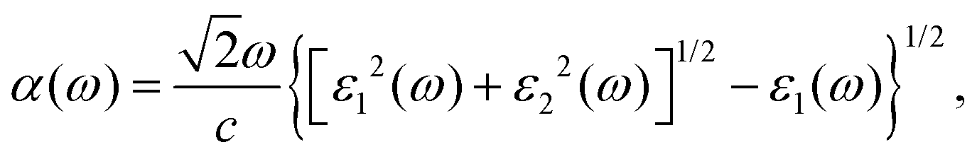
3.3 Optical properties
All these investigated 2D materials possess a decent bandgap of about 2.08–2.65 eV, which falls in the visible light region (the energies of the visible light spectrum vary from about 1.5 to 3.0 eV). Thus, it is necessary to evaluate the optical properties of these 2D XM to access its potential in optoelectronic devices. We calculated the optical absorption as follows:96| |  | (3) |
where α, ω and c are the absorption coefficient, angular frequency and the speed of light respectively. ε1(ω) and ε2(ω) are the real and imaginary parts of the dielectric constant, respectively. ε2(ω) can be obtained as follows:97| |  | (4) |
where Ψk, Ek and û are the wave function, energy and unit vector of the electric field of the incident light. The superscripts (v and c) in Ψk, Ek, label the conduction bands and valence bands, respectively. The complex dielectric function is ε(ω) = ε1(ω) + iε2(ω), and the real part ε1 can be obtained from ε2 by using the Kramers–Kronig relation. Considering the characteristic of 2D materials, we just investigated the in-plane light absorption properties (a-polarized and b-polarized light). Fig. 8 shows the absorption spectrum of the monolayer XM, which indicates that all these four XM materials strongly absorb a-polarized and b-polarized light around an energy of 3–5 eV. The areas below the adsorption profiles in the visible light region (about 1.64–3.19 eV) are 54.56 eV cm−1 (or 54.27 eV cm−1), 58.87 eV cm−1 (or 58.21 eV cm−1), 51.05 eV cm−1 (or 50.83 eV cm−1) and 55.53 eV cm−1 (or 55.20 eV cm−1) for GeS, GeSe, SiS and SiSe monolayers in the a-direction (or b-direction), respectively. Importantly, the GeSe and SiSe monolayers strongly absorb a-polarized and b-polarized light at around 2 eV but is transparent for GeS and SiS monolayers in this energy region. The optical absorption peak frequency is lower than that of δ-CTe.98 GeSe (or SiSe) monolayers have ultra-strong optical absorption, the maximal absorption coefficients are 7.69 × 105 cm−1 (or 7.8 × 105 cm−1) and 8.34 × 105 cm−1 (or 6.77 × 105 cm−1) for a-polarized and b-polarized light, respectively, and the positions of absorption peaks are 3.68 eV (or 2.91 eV) and 3.72 eV (or 3.30 eV). The characteristic that monolayer XM possesses different light absorption performances in different polarization directions is induced by the anisotropic crystal structure, which also raises up promising applications in ultraviolet region linear polarizers. Besides, the calculated optical absorption of GeS, GeSe, SiS and SiSe monolayers covers the entire solar spectrum, which suggests the potential importance in the application of solar photovoltaics. Furthermore, it is worth noting that the calculated optical absorption values are similar to that of monolayer MoS2, which has been reported to possess more than 5% solar power conversion efficiency in previous experimental investigation.99 The obtained light absorption coefficient is also higher than other commonly studied 2D materials such as MoSSe (about 5.5 × 105 cm−1),100 Hf2CO2 (about 4.8 × 105 cm−1),101 arsenene (about 2.7 × 105 cm−1),102 WSSe (about 2.1 × 105 cm−1)103 and δ-CS (about 5.8 × 105 cm−1),77 which were calculated using the similar method. In addition, it is worth noting that the GW + BSE method has been considered as an effective means to include the electron–hole interaction in the calculation of optical properties, which has been adopted in previous reports.104,105 However, the optical calculations with the GW method for our studied system are computationally expensive, and hence, we adopted the HSE06 calculation, which has also been adopted to explore the optical properties of 2D materials.106–108
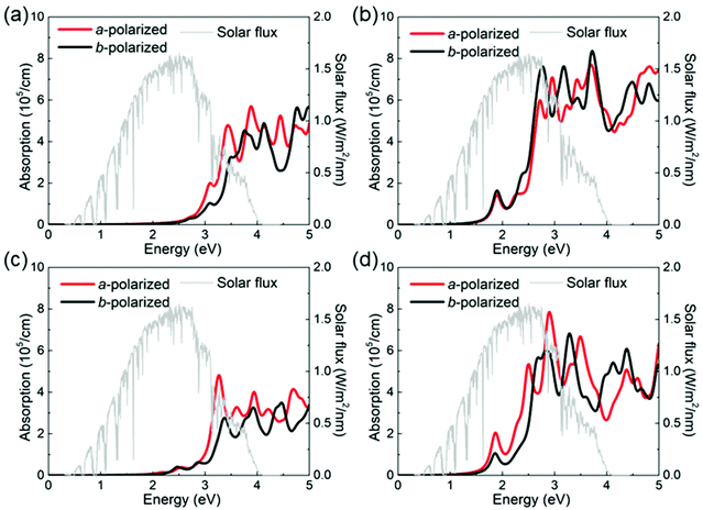 |
| | Fig. 8 Absorption spectrum of (a) GeS, (b) GeSe, (c) SiS and (d) SiSe monolayers, respectively. The red and black lines denote the absorption of a-polarized and b-polarized light, respectively. | |
4. Conclusions
In summary, based on DFT calculations, GeS, GeSe, SiS and SiSe monolayers were investigated to possess a puckered structure. The dynamic and thermal stability proves by AIMD simulations for those layered materials, and they also have a desirable bandgap of about 2.08–2.65 eV. The anisotropy mechanical properties were explored by in-plane Young's moduli and Poisson's ratios, and the novel NPR was obtained by −0.081 to −0.290 especially. Furthermore, the ultra-strong light absorption performance was addressed, and all those suggest that the studied δ-IV–VI monolayers can be considered as promising candidates for future nanoelectronic, nanomechanical and optoelectronic devices.
Conflicts of interest
There are no conflicts to declare.
Acknowledgements
This investigation was supported by the Open Fund Project of Maanshan Engineering Technology Research Center of Advanced Design for Automotive Stamping Dies (grant number: QMSG202105). We thank Dr Minglei Sun for fruitful discussions.
References
- A. K. Geim and K. S. Novoselov, The rise of graphene, Nat. Mater., 2007, 6, 183–191 CrossRef CAS PubMed.
- D. Jariwala, V. K. Sangwan, L. J. Lauhon, T. J. Marks and M. C. Hersam, Carbon nanomaterials for electronics, optoelectronics, photovoltaics, and sensing, Chem. Soc. Rev., 2013, 42, 2824–2860 RSC.
- E. Cadelano and L. Colombo, Effect of hydrogen coverage on the Young's modulus of graphene, Phys. Rev. B: Condens. Matter Mater. Phys., 2012, 85, 245434 CrossRef.
- E. Cadelano, P. L. Palla, S. Giordano and L. Colombo, Elastic properties of hydrogenated graphene, Phys. Rev. B: Condens. Matter Mater. Phys., 2010, 82, 235414 CrossRef.
- H. Zhang, Z. Duan, X. Zhang, C. Liu, J. Zhang and J. Zhao, Strength and fracture behavior of graphene grain boundaries: effects of temperature, inflection, and symmetry from molecular dynamics, Phys. Chem. Chem. Phys., 2013, 15, 11794–11799 RSC.
- J. Wang, R. Zhao, M. Yang, Z. Liu and Z. Liu, Inverse relationship between carrier mobility and bandgap in graphene, J. Chem. Phys., 2013, 138, 084701 CrossRef PubMed.
- Y. Cheng, X. Wu, Z. Zhang, Y. Sun, Y. Zhao, Y. Zhang and G. Zhang, Thermo-mechanical correlation in two-dimensional materials, Nanoscale, 2021, 13, 1425–1442 RSC.
- G. Qin, Q. B. Yan, Z. Qin, S. Y. Yue, M. Hu and G. Su, Anisotropic intrinsic lattice thermal conductivity of phosphorene from first principles, Phys. Chem. Chem. Phys., 2015, 17, 4854–4858 RSC.
- L. C. Zhang, G. Qin, W. Z. Fang, H. J. Cui, Q. R. Zheng, Q. B. Yan and G. Su, Tinselenidene: a Two-dimensional Auxetic Material with Ultralow Lattice Thermal Conductivity and Ultrahigh Hole Mobility, Sci. Rep., 2016, 6, 19830 CrossRef CAS PubMed.
- K. Ren, H. Qin, H. Liu, Y. Chen, X. Liu and G. Zhang, Manipulating Interfacial Thermal Conduction of 2D Janus Heterostructure via a Thermo-Mechanical Coupling, Adv. Funct. Mater., 2022, 2110846 CrossRef CAS.
- M. Sun, W. Tang, Q. Ren, Y. Zhao, S. Wang, J. Yu, Y. Du and Y. Hao, Electronic and magnetic behaviors of graphene with 5d series transition metal atom substitutions: A first-principles study, Phys. E, 2016, 80, 142–148 CrossRef CAS.
- P. Miro, M. Audiffred and T. Heine, An atlas of two-dimensional materials, Chem. Soc. Rev., 2014, 43, 6537–6554 RSC.
- Z. Luo, J. Maassen, Y. Deng, Y. Du, R. P. Garrelts, M. S. Lundstrom, D. Y. Peide and X. Xu, Anisotropic in-plane thermal conductivity observed in few-layer black phosphorus, Nat. Commun., 2015, 6, 1–8 Search PubMed.
- G. Zhang and Y.-W. Zhang, Thermal properties of two-dimensional materials, Chin. Phys. B, 2017, 26, 034401 CrossRef.
- K. Ren, X. Liu, S. Chen, Y. Cheng, W. Tang and G. Zhang, Remarkable Reduction of Interfacial Thermal Resistance in Nanophononic Heterostructures, Adv. Funct. Mater., 2020, 2004003 CrossRef CAS.
- Y. Cai, S. Chen, J. Gao, G. Zhang and Y. W. Zhang, Evolution of intrinsic vacancies and prolonged lifetimes of vacancy clusters in black phosphorene, Nanoscale, 2019, 11, 20987–20995 RSC.
- Y. Cai, Q. Ke, G. Zhang, B. I. Yakobson and Y. W. Zhang, Highly Itinerant Atomic Vacancies in Phosphorene, J. Am. Chem. Soc., 2016, 138, 10199–10206 CrossRef CAS PubMed.
- L. Xia, Z. Yang, B. Tang, F. Li, J. Wei and Z. Zhou, Carbon Nanofibers with Embedded Sb2Se3 Nanoparticles as Highly Reversible Anodes for Na-Ion Batteries, Small, 2021, 17, 2006016 CrossRef CAS PubMed.
- C. C. He, S. G. Xu, Y. J. Zhao, H. Xu and X. B. Yang, All-boron planar ferromagnetic structures: from clusters to monolayers, Nanoscale, 2021, 13, 9881–9887 RSC.
- Y. Liu, Q. Liu, Y. Liu, X. Jiang, X. Zhang and J. Zhao, Effects of spin-phonon coupling on two-dimensional ferromagnetic semiconductors: a case study of iron and ruthenium trihalides, Nanoscale, 2021, 13, 7714–7722 RSC.
- S. Ghosh, N. Stojic and N. Binggeli, Overcoming the asymmetry of the electron and hole doping for magnetic transitions in bilayer CrI3, Nanoscale, 2021, 13, 9391–9401 RSC.
- T. T. Dorini, F. Brix, C. Chatelier, A. Kokalj and E. Gaudry, Two-dimensional oxide quasicrystal approximants with tunable electronic and magnetic properties, Nanoscale, 2021, 13, 10771–10779 RSC.
- Y. Xu, J. Dai and X. C. Zeng, Al2C Monolayer Sheet and Nanoribbons with Unique Direction-Dependent Acoustic-Phonon-Limited Carrier Mobility and Carrier Polarity, J. Phys. Chem. Lett., 2016, 7, 302–307 CrossRef CAS PubMed.
- Q. Wu, W. W. Xu, B. Qu, L. Ma, X. Niu, J. Wang and X. C. Zeng, Au6S2 monolayer sheets: metallic and semiconducting polymorphs, Mater. Horiz., 2017, 4, 1085–1091 RSC.
- B. Li, J. Geng, H. Ai, Y. Kong, H. Bai, K. H. Lo, K. W. Ng, Y. Kawazoe and H. Pan, Design of 2D materials – MSi2CxN4-x (M = Cr, Mo, and W; x = 1 and 2) – with tunable electronic and magnetic properties, Nanoscale, 2021, 13, 8038–8048 RSC.
- S. Wang, N. Miao, K. Su, V. A. Blatov and J. Wang, Discovery of intrinsic two-dimensional antiferromagnets from transition-metal borides, Nanoscale, 2021, 13, 8254–8263 RSC.
- L. Liu, Z. Lin, J. Hu and X. Zhang, Full quantum search for high Tc two-dimensional van der Waals ferromagnetic semiconductors, Nanoscale, 2021, 13, 8137–8145 RSC.
- M. E. Kilic and K. R. Lee, Novel two-dimensional tetrahexagonal boron nitride with a sizable band gap and a sign-tunable Poisson's ratio, Nanoscale, 2021, 13, 9303–9314 RSC.
- X. Ma, T. Yang, D. Li and Y. Feng, Phase stability of monolayer Si1-xGex alloys with a Dirac cone, Nanoscale, 2021, 13, 8607–8613 RSC.
- J. J. Zhang, T. Altalhi, J. H. Yang and B. I. Yakobson, Semiconducting alpha′-boron sheet with high mobility and low all-boron contact resistance: a first-principles study, Nanoscale, 2021, 13, 8474–8480 RSC.
- J. Guan, X. Zhang, Q. Li, K. Deng, P. Jena and E. Kan, Two-dimensional metal-free boron chalcogenides B2X3 (X = Se and Te) as photocatalysts for water splitting under visible light, Nanoscale, 2021, 13, 3627–3632 RSC.
- X. Zhang, A. Chen, L. Chen and Z. Zhou, 2D Materials Bridging Experiments and Computations for Electro/Photocatalysis, Adv. Energy Mater., 2021, 2003841 Search PubMed.
- W. Li, Y. She, A. S. Vasenko and O. V. Prezhdo, Ab initio nonadiabatic molecular dynamics of charge carriers in metal halide perovskites, Nanoscale, 2021, 13, 10239–10265 RSC.
- S. Haastrup, M. Strange, M. Pandey, T. Deilmann, P. S. Schmidt, N. F. Hinsche, M. N. Gjerding, D. Torelli, P. M. Larsen and A. C. Riis-Jensen, The Computational 2D Materials Database: high-throughput modeling and discovery of atomically
thin crystals, 2D Mater., 2018, 5, 042002 CrossRef CAS.
- R. Lakes, Foam structures with a negative Poisson's ratio, Science, 1987, 235, 1038–1041 CrossRef CAS PubMed.
- R. Lakes, Advances in negative Poisson's ratio materials, Adv. Mater., 1993, 5, 293–296 CrossRef CAS.
- G. N. Greaves, A. L. Greer, R. S. Lakes and T. Rouxel, Poisson's ratio and modern materials, Nat. Mater., 2011, 10, 823–837 CrossRef CAS PubMed.
- X. Ren, R. Das, P. Tran, T. D. Ngo and Y. M. Xie, Auxetic metamaterials and structures: a review, Smart Mater. Struct., 2018, 27, 023001 CrossRef.
- J. Choi and R. Lakes, Non-linear properties of metallic cellular materials with a negative Poisson's ratio, J. Mater. Sci., 1992, 27, 5375–5381 CrossRef CAS.
- Y. J. Park and J. K. Kim, The effect of negative Poisson's ratio polyurethane scaffolds for articular cartilage tissue engineering applications, Adv. Mater. Sci. Eng., 2013, 2013, 853289 Search PubMed.
- X. Xu, Q. Zhang, M. Hao, Y. Hu, Z. Lin, L. Peng, T. Wang, X. Ren, C. Wang and Z. Zhao, Double-negative-index ceramic aerogels for thermal superinsulation, Science, 2019, 363, 723–727 CrossRef CAS PubMed.
- R. H. Baughman, J. M. Shacklette, A. A. Zakhidov and S. Stafström, Negative Poisson's ratios as a common feature of cubic metals, Nature, 1998, 392, 362–365 CrossRef CAS.
- Y. Sun and N. Pugno, Hierarchical fibers with a negative Poisson's ratio for tougher composites, Materials, 2013, 6, 699–712 CrossRef CAS PubMed.
- K. L. Alderson, A. Fitzgerald and K. E. Evans, The strain dependent indentation resilience of auxetic microporous polyethylene, J. Mater. Sci., 2000, 35, 4039–4047 CrossRef CAS.
- A. W. Lipsett and A. I. Beltzer, Reexamination of dynamic problems of elasticity for negative Poisson's ratio, J. Acoust. Soc. Am., 1988, 84, 2179–2186 CrossRef.
- R. C. Cammarata, Surface and interface stress effects in thin films, Prog. Surf. Sci., 1994, 46, 1–38 CrossRef CAS.
- J.-W. Jiang, S. Y. Kim and H. S. Park, Auxetic nanomaterials: Recent progress and future development, Appl. Phys. Rev., 2016, 3, 041101 Search PubMed.
- X. Ma, J. Liu, Y. Fan, W. Li, J. Hu and M. Zhao, Giant negative Poisson's ratio in two-dimensional V-shaped materials, Nanoscale Adv., 2021, 3, 4554–4560 RSC.
- J. Dagdelen, J. Montoya, M. de Jong and K. Persson, Computational prediction of new auxetic materials, Nat. Commun., 2017, 8, 323 CrossRef PubMed.
- J.-W. Jiang and H. S. Park, Negative Poisson's ratio in single-layer black phosphorus, Nat. Commun., 2014, 5, 4727 CrossRef CAS PubMed.
- Y. Du, J. Maassen, W. Wu, Z. Luo, X. Xu and P. D. Ye, Auxetic Black Phosphorus: A 2D Material with Negative Poisson's Ratio, Nano Lett., 2016, 16, 6701–6708 CrossRef CAS PubMed.
- H. Wang, X. Li, P. Li and J. Yang, δ-Phosphorene: a two dimensional material with a highly negative Poisson's ratio, Nanoscale, 2017, 9, 850–855 RSC.
- B. Wang, Q. Wu, Y. Zhang, L. Ma and J. Wang, Auxetic B4N Monolayer: A Promising 2D Material with in-Plane Negative Poisson's Ratio and Large Anisotropic Mechanics, ACS Appl. Mater. Interfaces, 2019, 11, 33231–33237 CrossRef CAS PubMed.
- J. H. Yuan, K. H. Xue, J. F. Wang and X. S. Miao, Gallium Thiophosphate: An Emerging Bidirectional Auxetic Two-Dimensional Crystal with Wide Direct Band Gap, J. Phys. Chem. Lett., 2019, 10, 4455–4462 CrossRef CAS PubMed.
- B. Zeng, M. Long, Y. Dong, J. Xiao, S. Zhang, Y. Yi and Y. Gao, Stress-sign-tunable Poisson's ratio in monolayer blue phosphorus oxide, J. Phys.: Condens. Matter, 2019, 31, 295702 CrossRef CAS PubMed.
- G. Qin and Z. Qin, Negative Poisson's ratio in two-dimensional honeycomb structures, npj Comput. Mater., 2020, 6, 51 CrossRef CAS.
- L. Yu, Q. Yan and A. Ruzsinszky, Negative Poisson's ratio in 1T-type crystalline two-dimensional transition metal dichalcogenides, Nat. Commun., 2017, 8, 15224 CrossRef CAS PubMed.
- C. Du, X. Hu, G. Zhang and Y. Cheng, 2D Materials Meet Biomacromolecules: Opportunities and Challenges, Acta Phys.-Chim. Sin., 2019, 35, 1078–1089 CAS.
- Z. Hu, Y. Ding, X. Hu, W. Zhou, X. Yu and S. Zhang, Recent progress in 2D group IV-IV monochalcogenides: synthesis, properties and applications, Nanotechnology, 2019, 30, 252001 CrossRef CAS PubMed.
- G. Qin, Z. Qin, W.-Z. Fang, L.-C. Zhang, S.-Y. Yue, Q.-B. Yan, M. Hu and G. Su, Diverse anisotropy of phonon transport in two-dimensional group IV–VI compounds: A comparative study, Nanoscale, 2016, 8, 11306–11319 RSC.
- P. Hu, L. Wang, M. Yoon, J. Zhang, W. Feng, X. Wang, Z. Wen, J. C. Idrobo, Y. Miyamoto, D. B. Geohegan and K. Xiao, Highly Responsive Ultrathin GaS Nanosheet Photodetectors on Rigid and Flexible Substrates, Nano Lett., 2013, 13, 1649–1654 CrossRef CAS PubMed.
- P. Hu, Z. Wen, L. Wang, P. Tan and K. Xiao, Synthesis of few-layer GaSe nanosheets for high performance photodetectors, ACS Nano, 2012, 6, 5988–5994 CrossRef CAS PubMed.
- R. K. Ulaganathan, Y.-Y. Lu, C.-J. Kuo, S. R. Tamalampudi, R. Sankar, K. M. Boopathi, A. Anand, K. Yadav, R. J. Mathew and C.-R. Liu, High photosensitivity and broad spectral response of multi-layered germanium sulfide transistors, Nanoscale, 2016, 8, 2284–2292 RSC.
- Y. Wei, J. He, Q. Zhang, C. Liu, A. Wang, H. Li and T. Zhai, Synthesis and investigation of layered GeS as a promising large capacity anode with low voltage and high efficiency in full-cell Li-ion batteries, Mater. Chem. Front., 2017, 1, 1607–1614 RSC.
- S. R. Tamalampudi, Y.-Y. Lu, U. Rajesh Kumar, R. Sankar, C.-D. Liao, C.-H. Cheng, F. C. Chou and Y.-T. Chen, High performance and bendable few-layered InSe photodetectors with broad spectral response, Nano Lett., 2014, 14, 2800–2806 CrossRef CAS PubMed.
- A. Okazaki, The crystal structure of germanium selenide GeSe, J. Phys. Soc. Jpn., 1958, 13, 1151–1155 CrossRef CAS.
- J. H. Yang, Y. Zhang, W. J. Yin, X. G. Gong, B. I. Yakobson and S. H. Wei, Two-Dimensional SiS Layers with Promising Electronic and Optoelectronic Properties: Theoretical Prediction, Nano Lett., 2016, 16, 1110–1117 CrossRef CAS PubMed.
- T. Jing, D. Liang, M. Deng and S. Cai, Two-dimensional IV–VI materials with in-plane negative Poisson's ratio and anisotropic carrier mobility, J. Mater. Chem. C, 2020, 8, 10382–10389 RSC.
- J.-H. Yang, Q. Yuan, H. Deng, S.-H. Wei and B. I. Yakobson, Earth-Abundant and Non-Toxic SiX (X = S, Se) Monolayers as Highly Efficient Thermoelectric Materials, J. Phys. Chem. C, 2017, 121, 123–128 CrossRef CAS.
- S. Karmakar, C. Chowdhury and A. Datta, Two-Dimensional Group IV Monochalcogenides: Anode Materials for Li-Ion Batteries, J. Phys. Chem. C, 2016, 120, 14522–14530 CrossRef CAS.
- C. Chowdhury, S. Karmakar and A. Datta, Monolayer Group IV–VI
Monochalcogenides: Low-Dimensional Materials for Photocatalytic Water Splitting, J. Phys. Chem. C, 2017, 121, 7615–7624 CrossRef.
- G. Kresse and D. Joubert, From ultrasoft pseudopotentials to the projector augmented-wave method, Phys. Rev. B: Condens. Matter Mater. Phys., 1999, 59, 1758 CrossRef CAS.
- J. Heyd, J. E. Peralta, G. E. Scuseria and R. L. Martin, Energy band gaps and lattice parameters evaluated with the Heyd-Scuseria-Ernzerhof screened hybrid functional, J. Chem. Phys., 2005, 123, 174101 CrossRef PubMed.
- G. Henkelman, B. P. Uberuaga and H. Jónsson, A climbing image nudged elastic band method for finding saddle points and minimum energy paths, J. Chem. Phys., 2000, 113, 9901–9904 CrossRef CAS.
- A. Togo and I. Tanaka, First principles phonon calculations in materials science, Scr. Mater., 2015, 108, 1–5 CrossRef CAS.
- A. Togo, F. Oba and I. Tanaka, First-principles calculations of the ferroelastic transition between rutile-type and CaCl2-type SiO2 at high pressures, Phys. Rev. B: Condens. Matter Mater. Phys., 2008, 78, 134106 CrossRef.
- M. Sun and U. Schwingenschlögl, δ-CS: A Direct-Band-Gap Semiconductor Combining Auxeticity, Ferroelasticity, and Potential for High-Efficiency Solar Cells, Phys. Rev. Appl., 2020, 14, 044015 CrossRef CAS.
- S. Dutta and G. Jeffrey, On the structure of germanium selenide and related binary IV/VI compounds, Inorg. Chem., 1965, 4, 1363–1366 CrossRef CAS.
- M. Sun and U. Schwingenschlögl, Structure Prototype Outperforming MXenes in Stability and Performance in Metal-Ion Batteries: A High Throughput Study, Adv. Energy Mater., 2021, 2003633 CrossRef CAS.
- Y. Mao, J. Ben, J. Yuan and J. Zhong, Tuning the electronic property of two dimensional SiSe monolayer by in-plane strain, Chem. Phys. Lett., 2018, 705, 12–18 CrossRef CAS.
- J. Gao, X. Liu, G. Zhang and Y. W. Zhang, Nanotube-terminated zigzag edges of phosphorene formed by self-rolling reconstruction, Nanoscale, 2016, 8, 17940–17946 RSC.
- S. Zhang, N. Wang, S. Liu, S. Huang, W. Zhou, B. Cai, M. Xie, Q. Yang, X. Chen and H. Zeng, Two-dimensional GeS with tunable electronic properties via external electric field and strain, Nanotechnology, 2016, 27, 274001 CrossRef PubMed.
- T. Hu and J. Dong, Two new phases of monolayer group-IV monochalcogenides and their piezoelectric properties, Phys. Chem. Chem. Phys., 2016, 18, 32514–32520 RSC.
- X. Lv, W. Wei, Q. Sun, F. Li, B. Huang and Y. Dai, Two-dimensional germanium monochalcogenides for photocatalytic water splitting with high carrier mobility, Appl. Catal., B, 2017, 217, 275–284 CrossRef CAS.
- S. P. Poudel and S. Barraza-Lopez, Metastable piezoelectric group-IV monochalcogenide monolayers with a buckled honeycomb structure, Phys. Rev. B, 2021, 103, 024107 CrossRef CAS.
- H. Yin, C. Liu, G.-P. Zheng, Y. Wang and F. Ren, Ab initio simulation studies on the room-temperature ferroelectricity in two-dimensional β-phase GeS, Appl. Phys. Lett., 2019, 114, 192903 CrossRef.
- Y. Hu, S. Zhang, S. Sun, M. Xie, B. Cai and H. Zeng, GeSe monolayer semiconductor with tunable direct band gap and small carrier effective mass, Appl. Phys. Lett., 2015, 107, 122107 CrossRef.
- S. Zhang, S. Liu, S. Huang, B. Cai, M. Xie, L. Qu, Y. Zou, Z. Hu, X. Yu and H. Zeng, Structural and electronic properties of atomically thin germanium selenide polymorphs, Sci. China Mater., 2015, 58, 929–935 CrossRef CAS.
- S. Nosé, A unified formulation of the constant temperature molecular dynamics methods, J. Chem. Phys., 1984, 81, 511–519 CrossRef.
- H. Yang, Y. Ma, S. Zhang, H. Jin, B. Huang and Y. Dai, GeSe@SnS: stacked Janus structures for overall water splitting, J. Mater. Chem. A, 2019, 7, 12060–12067 RSC.
- S. Shen, Y. Ma, H. Wang, B. Huang and Y. Dai, Single-Layer PtI2: A Multifunctional Material with Promising Photocatalysis toward the Oxygen Evolution Reaction and Negative Poisson's Ratio, ACS Appl. Mater. Interfaces, 2019, 11, 31793–31798 CrossRef CAS PubMed.
- R. Peng, Y. Ma, Z. He, B. Huang, L. Kou and Y. Dai, Single-Layer Ag2S: A Two-Dimensional Bidirectional Auxetic Semiconductor, Nano Lett., 2019, 19, 1227–1233 CrossRef CAS PubMed.
- X. Kong, J. Deng, L. Li, Y. Liu, X. Ding, J. Sun and J. Z. Liu, Tunable auxetic properties in group-IV monochalcogenide monolayers, Phys. Rev. B, 2018, 98, 184104 CrossRef.
- B. Liu, M. Niu, J. Fu, Z. Xi, M. Lei and R. Quhe, Negative Poisson's ratio in puckered two-dimensional materials, Phys. Rev. Mater., 2019, 3, 054002 CrossRef CAS.
- L. Yu, Z. Qin, H. Wang, X. Zheng and G. Qin, Half-negative Poisson's ratio in graphene+ with intrinsic Dirac nodal loop, Cell Rep. Phys. Sci., 2022, 3, 100790 CrossRef CAS.
- M. Sun, J.-P. Chou, J. Gao, Y. Cheng, A. Hu, W. Tang and G. Zhang, Exceptional Optical Absorption of Buckled Arsenene Covering a Broad Spectral Range by Molecular Doping, ACS Omega, 2018, 3, 8514–8520 CrossRef CAS PubMed.
- G. Zhang, M.-B. Yu, C.-H. Tung and G.-Q. Lo, Quantum Size Effects on Dielectric Constants and Optical Absorption of Ultrathin Silicon Films, IEEE Electron Device Lett., 2008, 29, 1302–1305 CAS.
- M. Sun and U. Schwingenschlögl, Unique Omnidirectional Negative Poisson's Ratio in δ-Phase Carbon Monochalcogenides, J. Phys. Chem. C, 2021, 125, 4133–4138 CrossRef CAS.
- M.-L. Tsai, S.-H. Su, J.-K. Chang, D.-S. Tsai, C.-H. Chen, C.-I. Wu, L.-J. Li, L.-J. Chen and J.-H. He, Monolayer MoS2 heterojunction solar cells, ACS Nano, 2014, 8, 8317–8322 CrossRef CAS PubMed.
- Z. Cui, N. Lyu, Y. Ding and K. Bai, Noncovalently functionalization of Janus MoSSe monolayer with organic molecules, Phys. E, 2021, 127, 114503 CrossRef CAS.
- K. Ren, R. Zheng, P. Xu, D. Cheng, W. Huo, J. Yu, Z. Zhang and Q. Sun, Electronic and Optical Properties of Atomic-Scale Heterostructure Based on MXene and MN (M = Al, Ga): A DFT Investigation, Nanomaterials, 2021, 11, 2236 CrossRef CAS PubMed.
- Z. Cui, M. Wang, N. Lyu, S. Zhang, Y. Ding and K. Bai, Electronic, magnetism and optical properties of transition metals adsorbed puckered arsenene, Superlattices Microstruct., 2021, 152, 106852 CrossRef CAS.
- Z. Zhu, K. Ren, H. Shu, Z. Cui, Z. Huang, J. Yu and Y. Xu, First-Principles Study of Electronic and Optical Properties of Two-Dimensional WSSe/BSe van der Waals Heterostructure with High Solar-to-Hydrogen Efficiency, Catalysts, 2021, 11, 991 CrossRef CAS.
- M. Bernardi, M. Palummo and J. C. Grossman, Extraordinary sunlight absorption and one nanometer thick photovoltaics using two-dimensional monolayer materials, Nano Lett., 2013, 13, 3664–3670 CrossRef CAS PubMed.
- M. Bruno, M. Palummo, A. Marini, R. Del Sole and S. Ossicini, From Si nanowires to porous silicon: the role of excitonic effects, Phys. Rev. Lett., 2007, 98, 036807 CrossRef PubMed.
- B.-J. Wang, X.-H. Li, X.-L. Cai, W.-Y. Yu, L.-W. Zhang, R.-Q. Zhao and S.-H. Ke, Blue Phosphorus/Mg(OH)2 van der Waals Heterostructures as Promising Visible-Light Photocatalysts for Water Splitting, J. Phys. Chem. C, 2018, 122, 7075–7080 CrossRef CAS.
- B.-J. Wang, X.-H. Li, R. Zhao, X.-L. Cai, W.-Y. Yu, W.-B. Li, Z.-S. Liu, L.-W. Zhang and S.-H. Ke, Electronic structures and enhanced photocatalytic properties of blue phosphorene/BSe van der Waals heterostructures, J. Mater. Chem. A, 2018, 6, 8923–8929 RSC.
- Q. Yang, C.-J. Tan, R.-S. Meng, J.-K. Jiang, Q.-H. Liang, X. Sun, D.-G. Yang and X.-P. Chen, AlN/BP heterostructure photocatalyst for water splitting, IEEE Electron Device Lett., 2017, 38, 145–148 CAS.
|
| This journal is © The Royal Society of Chemistry 2022 |
Click here to see how this site uses Cookies. View our privacy policy here. 
 a,
Xikui
Ma
b,
Xiangjun
Liu
a,
Xikui
Ma
b,
Xiangjun
Liu