
 Open Access Article
 This Open Access Article is licensed under a
 Creative Commons Attribution 3.0 Unported Licence
Nanoscale electrochemical 3D deposition of cobalt with nanosecond voltage pulses in an STM†
Alain
Reiser‡
 a,
Rolf
Schuster
b and
Ralph
Spolenak
*a
a,
Rolf
Schuster
b and
Ralph
Spolenak
*a
aLaboratory for Nanometallurgy, Department of Materials, Federal Institute of Technology (ETH) Zürich, 8093 Zürich, Switzerland. E-mail: ralph.spolenak@mat.ethz.ch
bInstitute of Physical Chemistry, Karlsruhe Institute of Technology, 76131 Karlsruhe, Germany
First published on 28th March 2022
Abstract
To explore a minimal feature size of <100 nm with electrochemical additive manufacturing, we use a strategy originally applied to microscale electrochemical machining for the nanoscale deposition of Co on Au. The concept's essence is the localization of electrochemical reactions below a probe during polarization with ns-long voltage pulses. As shown, a confinement that exceeds that predicted by a simple model based on the time constant for one-dimensional double layer charging enables a feature size of <100 nm for 2D patterning. We further indirectly verify the potential for out-of-plane deposition by tracking growth curves of high-aspect-ratio deposits. Importantly, we report a lack of anodic stability of Au tips used for patterning. As an inert probe is the prerequisite for controlled structuring, we experimentally verify an increased resistance of Pt probes against degradation. Consequently, the developed setup and processes show a path towards reproducible direct 2D and 3D patterning of metals at the nanoscale.
Introduction
Nanoscale additive manufacturing (AM) of inorganic materials offers exciting prospects for nanomanufacturing, enabling 3D structures for sensing1,2 or plasmonic3 applications, or additive synthesis of multi-materials with extremely high resolution.4 Yet, the deposition of metals of high purity with a resolution <100 nm is challenging with current AM methods.5 Materials grown by focused electron/ion-beam-induced deposition (FEBID/FIBID) using conventional precursors notoriously suffer from high carbon contents,6 although high metal contents have been enabled by the use of UHV systems7 (>95% Fe) or carbon-free but unstable precursors like gold-trifluorophosphine-chloride.8 Post-growth purification often results in shrinkage and warping of structures (chemical purification with high geometric fidelity has recently been demonstrated for needle-like structures3). Techniques based on dispensing of nanoparticle inks suffer from similar complications during post-print thermal annealing, with evolution of porosity and warping being a common issue.9,10 In addition, ink-based methods are limited to a feature size larger than a few particle diameters due to clogging issues—with smallest particle diameters of a few nanometers, minimum line widths of several tens of nanometers can probably not be expected (currently, the smallest line width of annealed inks is 80 nm,11 and direct ink writing (DIW) achieves minimal line widths of 0.6–2 μm![[thin space (1/6-em)]](https://www.rsc.org/images/entities/char_2009.gif) 12). To avoid potentially damaging post-deposition procedures, direct metal deposition is advantageous. However, not many direct-deposition techniques can possibly reach the length scale in question. The low transfer accuracy of laser-induced forward transfer (LIFT) renders advances towards nanoscale patterning extremely challenging. As much needed alternatives, electrochemical methods—deposition of pure metals from particle-free salt solutions, using nanometer probes to guarantee accuracy and resolution—may offer a pathway to nanoscale 3D deposition of high-purity metals with access to the 10 nm-regime. Indeed, recent developments in electrochemical AM methods demonstrate a feature size smaller than 100 nm.4,13
12). To avoid potentially damaging post-deposition procedures, direct metal deposition is advantageous. However, not many direct-deposition techniques can possibly reach the length scale in question. The low transfer accuracy of laser-induced forward transfer (LIFT) renders advances towards nanoscale patterning extremely challenging. As much needed alternatives, electrochemical methods—deposition of pure metals from particle-free salt solutions, using nanometer probes to guarantee accuracy and resolution—may offer a pathway to nanoscale 3D deposition of high-purity metals with access to the 10 nm-regime. Indeed, recent developments in electrochemical AM methods demonstrate a feature size smaller than 100 nm.4,13
To evaluate options for further decreasing the minimal feature size of electrochemical concepts, it is helpful to consider the current limitations of state-of-the-art techniques for 2D and 3D patterning, which include nozzle-based methods (all current AM concepts) and tip-based methods (up to date used for 2D patterning only). The nozzle-based concepts have shown smallest 3D feature size of ≥25 nm (meniscus-confined electrodeposition, MCED) and ≈100 nm4 (electrohydrodynamic redox printing, EHD-RP). In first approximation, the feature size of MCED is equal to the diameter of the capillary. The minimal feature size to be achieved with current feedback principles is estimated to be 25 nm, with smaller feature size prohibited by experimentally challenging prevention of nozzle clogging.13 In EHD-RP, a mere decrease of nozzle aperture from 160 to 100 nm did not result in a decreased but rather increased feature size.4 A third approach, concentration-confined electrodeposition,14 is presently unsuitable for nanoscale deposition due to the poor confinement of deposition—the use of apertures as small as 30–50 nm merely decreased the feature size to 400–600 nm.15
In contrast, electrochemical 2D patterning with nanoscale-sharp tips (as those typically used in scanning probe microscopy, SPM) enables a feature size close to 10 nm—the smallest feature size demonstrated was 16 nm for Co deposits16 and ≈10 nm for Cu.17 Importantly, the absence of a clogging issue with scanning probes guarantees minimal dimensions of the structuring tools and thus the potential for smallest feature sizes. However, the localization of electrodeposition and the supply of ions is less straightforward than with capillary-based printing nozzles. Of the methods suggested in literature, dip-pen lithography18 is the only air-based technique, supplying ions through a liquid meniscus between substrate and an atomic force microscope (AFM) tip (similar to the meniscus used in MCED). Localization of deposition in the meniscus is straightforward, but the limited reservoir of ions (metal salts dried on the AFM tip) is not ideal for continuous deposition. As a consequence, the majority of proposed techniques relies on the supply of ions from a bath of electrolyte solution. Immersing the probe and the substrate into a solution of metal salts guarantees a practically infinite supply of cations for electrodeposition, but demands more advanced strategies for localization of the electrodeposition. The proposed concepts for localized growth below a SPM tip immersed in an electrolyte bath can be grouped into two fundamental categories: first, the limitation of the active surface area, and second, a local modification of the factors that govern either the current distribution, the kinetics or the energetics of the electrochemcial reaction. The first group is not suited for 3D deposition, as it merely relies on the local activation of a generally passivated substrate19—an approach that is limited to deposition directly on the substrate and offers no means for out-of-plane growth. In the second group, methods that utilize the inhomogeneous current distribution below a tip suffer from low resolution (a minimal feature size of 2 μm was achieved by using the tip as a local anode upon direct current electrodeposition20), and methods that locally introduce surface defects for preferential nucleation21,22 show an inability for 3D deposition. The only concepts that guarantee strict localization of the deposition (and thus high resolution) in combination with no need for modifications of the substrate (and thus the possibility to enter the third dimension) are those that energetically limit the spatial extent of cathodic reactions. Energetic localization of electrochemical deposition is based on a local increase of the activation or concentration overpotential. The approach guarantees strong confinement due to the exponential relationship between growth rate and overpotential. Two concepts that make use of the exponential confinement have demonstrated deposition of metals with nanometric resolution. The first is based on the manipulation of the local Nernst potential,16 and the second relies on spatially containing the charging of the cathode's double-layer capacitance by nanosecond voltage pulses.23 While we have experimentally studied both strategies, we have more successfully implemented the second approach and thus think it is a more robust pathway towards 3D deposition with an electrochemical STM—probably due to its relaxed requirements to the stability of the substrate's potential (approximately ±100 mV versus 20 mV) and the possibility to use electrolytes of high concentration (1 M versus 1 mM).
The concept of confinement by spatial limitation of double-layer charging is illustrated best with the simplified equivalent circuits for two current paths (1) and (2) that connect tip and substrate in Fig. 1a. Typically, the surface potential of a conductive electrode immersed in an electrolyte solution, that is, the voltage drop across its electrochemical double layer (DL), is constant across a well conductive electrode's expanse. Yet, the application of nanosecond voltage pulses between the tip and the substrate results in an effective confinement of current flow through path (1) and hence a localization of double-layer polarization and all electrochemical reactions to regions connected by this path. The confinement originates from varying time constants τ = RC = ρd × cDL that describe the transient voltage UC(t) for each of the current paths upon pulsing the potential U applied between tip and substrate. As the double layer capacitance per area cDL and the specific electrolyte resistance ρ can be assumed to be constant, τ(d) is directly proportional to the local distance d to the tip and τ1 < τ2. Additionally, UC(t) becomes a function of not only t but also d. During a voltage pulse of duration tp, the local polarization UC(d) reaches significant values only if the local τ(d) is on the order of the pulse width tp, strongly confining electrochemical reactions to areas close to the tip (and making the amount of confinement proportional to the pulse length). A pulse width of 30 ns is estimated to limit polarization within a distance d of approximately 1 μm in a typical aqueous electrolyte solution (0.1 M HClO4),23 or d = 200 nm in a non-aqueous solution with lower conductivity (1 M LiCl in DMSO)24. The concept has mainly been used for micromachining of various metals and p/Si with minimal gap widths between tool and trench down to 20 nm.23,25,26 Demonstrations of the reverse process deposition of micrometer-sized Cu-islands (using a micrometer-sized tool)23 and ≈10 nm-wide Cu dots (with an STM tip)17—showed a potential for unrivaled minimal feature sizes in electrochemical AM. Yet, no 3D deposition has been reported so far, and even the mentioned reports of 2D deposition have a character of preliminary results.
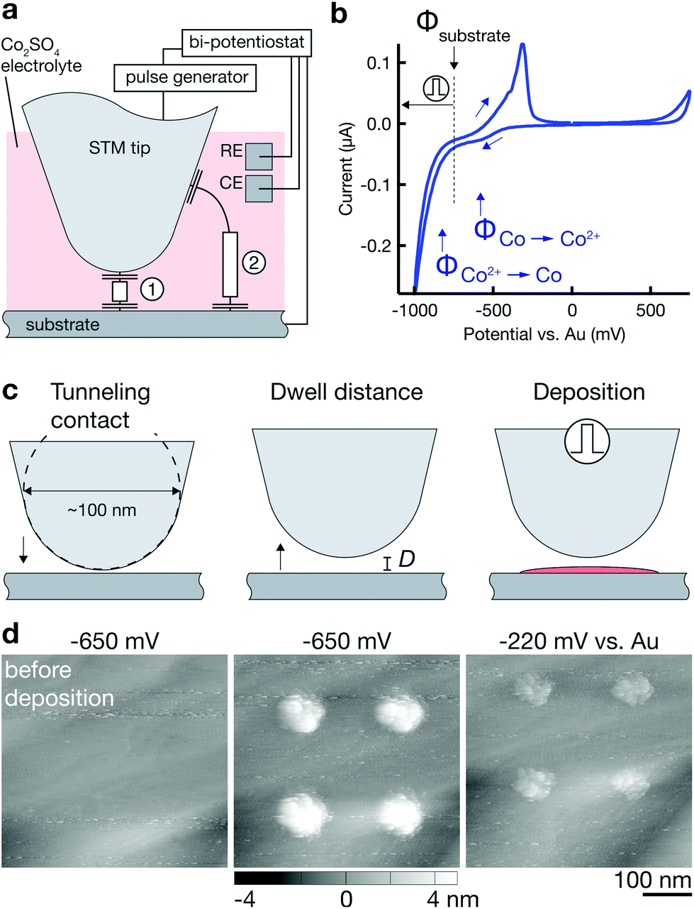 | ||
| Fig. 1 Localized Co deposition by nanosecond voltage pulses. (a) Schematic of the experimental setup for localized electrochemical deposition. Current paths (1) and (2) are representative of paths with low (1) and high (2) time constant for DL charging τ = RC = ρd × cDL. Application of nanosecond voltage pulses limits charging of the substrate's DL to regions connected by current path (1). (b) Cyclic voltammogram of a Au substrate in a solution of 1 M CoSO4 in DMSO. During and after deposition, the substrate potential Φsubstrate is potentiostatically set to ΦCo2+→Co < Φsubstrate < ΦCo→Co2+, preventing delocalized deposition of Co as well as dissolution of local Co deposits. Upon application of positive nanosecond voltage pulses to the tip, the substrate is locally polarized towards more negative potentials, initiating local Co deposition. (c) Schematic of the deposition procedure (drawn to scale). Tip and substrate are immersed in a Co2+-containing electrolyte solution. The tip is positioned at a defined dwell distance d from the substrate by approach of the tip until tunneling contact and subsequent retraction by a distance d (typically, d = 10 nm). Application of nanosecond voltage pulses (10–100 ns) to the tip locally polarizes the substrate below the tip and initiates deposition. (d) Deposition is verified by pre- and post-deposition scans of the substrate. STM scans of a Au surface before and after four deposition events, and after increasing the surface potential to a value Φsubstrate > ΦCo→Co2+. The incomplete dissolution suggests that the deposits were mostly Co but contained Au contamination due to a degrading tip. Surface potentials (vs. Au) are stated above the images. Deposition parameters. Electrolyte: 1 M CoSO4 in DMSO; pulse length: 100 ns; pulse amplitude: 6 V; duty cycle: 0.01; pulses per point: 3000; dwell distance: 10 nm; tip: Au. | ||
Here, we explore possibilities for nanoscale 3D deposition with nanosecond voltage pulses, motivated by the fact that this approach has shown smallest 2D feature sizes amongst all electrochemical AM techniques. With a goal of evaluating the feasibility of the approach for 2D and 3D deposition, we demonstrate reproducible 2D patterning and out-of-plane growth using nanosecond voltage pulses to localize the deposition in an electrochemical STM. Utilizing STM probes as tools for local deposition, we demonstrate sub-100 nm 2D-structuring of Co on Au in a DMSO electrolyte. Importantly, we find that the achieved feature size is not explained by the limited spatial extent of charging of the double layer alone, and additional kinetic or energetic mechanisms must be responsible for the localization of deposition. We further discuss challenges for 3D deposition and reproducibility (in aqueous and non-aqueous solvents), both related to the electrochemical stability of the used metallic STM tips. As a result, we show improved inertness of Pt or Pt-20 at% Ir probes in aqueous electrolytes. With improved reproducibility and proof-of-concept demonstrated here, future exploration of the method for direct out-of-plane deposition offers the potential for a simple, economic alternative to FEBID for applications that need high purity of metals.
Methods section
Electrochemical STM and pulse setup
A schematic of the custom-built setup for additive deposition with nanosecond voltage pulses is shown in the electronic supplementary information (ESI) Fig. S1.† The setup is composed of three subsystems: an STM (Cypher-AFM in STM-mode, Asylum Research, USA) combined with a custom-built electrochemical cell, a bi-potentiostat (PGUmicro, IPS, Germany) and a pulse pattern generator (2x81111A, Agilent, USA). The purpose of the STM is twofold: first, it controls the movement of the substrate relative to the tip in three dimensions during deposition. Second, it provides the tunneling current as a position feedback signal. This feedback allows the positioning of the tip before and during deposition with sub-nanometer precision. The bi-potentiostat controls the average potentials of the tip and the substrate—both immersed in an electrolyte solution—versus the reference electrode and thereby governs global, non-localized electrochemical reactions. Additionally, it monitors the corresponding faradaic currents. In contrast, the pulse generator controls the potential of the tip and the substrate at MHz-rates, inducing localized electrochemical reactions under the tip. The pulse amplitude and the pulse current are monitored with an oscilloscope (6404D, PicoScope, England). It is important to note that the measurement grounds of the three subsystems are held at the same level to avoid leakage currents between the individual instruments. This is achieved on a hardware level by shorting the BNC ground connections of the instruments and by isolating the bi-potentiostat from mains earth using an isolation transformer.The setup operates in two distinct modes that cannot run simultaneously, namely a feedback mode and a pulse mode. In feedback mode, the STM tip is connected to the input of the STM current amplifier. This enables the monitoring of the tunneling current and hence precise positioning of the tip. The tunneling voltage is equal to the potential of the tip (working electrode 1, WE1) and the surface potential of the substrate (WE2). In pulse mode, the tip is routed to the output of the pulse generator, so that voltage pulses can be applied to the tip. A mechanical relay switch (ESI Fig. S1a, (2)†) switches the electrical connection of the tip between the STM current input and the pulse generator as required. In either position of the switch, the rest potential of the tip is virtual ground.
The current circuits for low- (blue) and high-frequency currents (red) are separated by appropriate high- and low-pass filters (ESI Fig. S1a, (4, 5)†). The low-frequency currents, representing global faradaic reactions, flow between the counter electrode (CE) and the tip (for faradaic reactions at the tip) or between the CE and the substrate connected to the WE2 input of the potentiostat (faradaic reactions at the substrate). The high-frequency current flows from (or into) the output of the pulse generator through the tip into the substrate and subsequently across a capacitance (high-pass filter, (4)) to ground. In order to minimize the interference of these two circuits, low-pass filters (5) are connected to RE, CE and WE2 in series (see Fig. S2† for a schematic of the electronic circuits).
The deposition procedure is computer controlled through a customized software developed in-house and programmed in the Igor Pro software environment (Wavemetrics). It facilitates point-wise or continuous deposition, implements a correction for substrate tilt, and enables recording of out-of-plane growth curves.
Chemicals and materials
The electrochemical cell was designed in-house and made from polychlorotrifluoroethylene (PCTFE, Cellpack, Switzerland). O-rings were purchased from Angst + Pfister (NORMATEC FKM 70, Switzerland). The counter- and quasi-reference-electrode were plain Au wires (0.1 mm diameter, Möller AG, Switzerland). All constituents of the cell and the electrodes were immersed in fresh piranha solution (3:1 volumetric mixture of H2SO4 (conc.):H2O2 (30%)) and subsequently rinsed with MilliQ water and stored in MilliQ water until used. Substrates were either Au single crystals ((111)-out-of-plane <1%, 99.999% purity, Mateck, Germany) or 100 nm thick Au films evaporated onto Si-wafers (including a Cr adhesion layer, 10 nm). Single crystals were flame-annealed in a propane-butane flame for 10 min preceding every experiment. After each experiment, the single crystals were cycled in 1 M aqueous H2SO4 to remove metallic residues.
Au STM tips were electrochemically etched from Au wires (0.25 mm diameter, 99.999%, Alfa Aesar, Germany) in a 1:1 volumetric solution of HCl (fuming) and ethanol. For etching, we used a potentiostat (PTSTAT12, Metrohm Autolab, Netherlands) to apply a positive DC potential of 2.4 V between a Pt counter-electrode and the Au wire. No current monitor or feedback mechanism to terminate etching was used. After etching, the tips were rinsed with MilliQ water and blown-dried. Typical radii of Au tips were 50 nm. Pt tips were etched from Pt wires (0.25 mm diameter, 99.997%, Alfa Aesar, Germany) in aq. NaOH solutions (DC or AC voltage profiles with various amplitudes (2–10 V)). Pt-20 at% Ir tips were purchased from NaugaNeedles, USA (NN-USPtIr-W250, nominal tip radius 25–50 nm). All STM tips were coated with a thermoplastic wax (Apiezon, England) to minimize the active surface area of the tips to approximately 50 μm2.
Electrolytes were prepared in glass vials previously cleaned in fresh piranha solution and thoroughly washed with MilliQ water. Typical concentrations were 1 and 2 M of CoSO4 (Heptahydrate, 99.999%, Alfa Aesar, Germany). The solvent was either MilliQ water or dimethyl sulfoxide (DMSO, analytical reagent grade, Fisher Scientific UK). The electrolyte was handled with sterile plastic Eppendorf pipette tips. All experiments were conducted under atmospheric conditions, without any purging of the electrolytes.
Analysis
The dimensions of the deposits were typically assessed in situ by STM imaging (typical parameters were: tunneling current: ≈1 nA, tunneling voltage: ≈200 mV, scan rate: 1–2 Hz). Section line profiles were always averaged over a width of 10 scan lines. SEM analysis was performed with a Magellan 400 SEM (FEI, USA).Results and discussion
The deposition procedure
Fig. 1 sketches the basic procedure for localized deposition of Co on a Au substrate utilizing a Au STM tip as a tool for initiating deposition. First, it is important to note that the surface potentials of the two working electrodes, Φtip and Φsubstrate, are continuously controlled by a low-frequency bi-potentiostat (versus a Au quasi-reference electrode, RE). Both electrodes are held at a potential that avoids any faradaic reactions related to the deposition or dissolution of Co. Typically, Φtip and Φsubstrate are selected to be in-between the onset potential of Co deposition ΦCo2+→Co and Co dissolution ΦCo→Co2+, as indicated in the cyclic voltammogram of the Au substrate in Fig. 1b (Φtip is ≈200 mV positive to Φsubstrate). The rationale for these potentials is simple: Φ < ΦCo2+→Co would result in continuous, non-localized electrodeposition of Co onto the substrate (or the tip); in contrast, Φ > ΦCo→Co2+ would lead to the immediate dissolution of any localized deposit.Prior to any deposition, an image of the substrate is recorded by scanning of the surface with the setup in feedback mode. For deposition, the tip is positioned 10–100 nm above the substrate by first approaching the surface until a tunneling current is detected (defined as “tunneling contact”) and then retracting the tip by the respective distance d into its dwell position (Fig. 1c). In this position, the setup is switched into pulse mode, i.e., the STM tip is connected to the output of the pulse generator. For deposition, a pulse train of a predefined number of pulses (typically 100–100000 pulses of 10–100 ns at a duty cycle of 0.01–0.1 and an amplitude of +1–6 V) is applied to the tip. As described in detail elsewhere,23,25,27 the high-frequency pulses are added to the baseline potential of the tip Φtip (and with opposite polarity to Φsubstrate), which results in a local decrease of the surface potential Φsubstrate to values <ΦCo2+→Co and initiates local growth. After deposition, the system is returned into feedback mode and the deposits are imaged. To judge whether the deposited material is Co, the surface potential is lifted to values Φsubstrate > ΦCo→Co2+. STM scans documenting such a deposition-dissolution cycle are shown in Fig. 1d. The dissolution of large fractions of the deposited material at Φsubstrate > ≈400 mV matches the behavior of Co predicted by the cyclic voltammogram in Fig. 1b and strongly suggests that the major constituent of the deposits is Co. Indeed, the deposition of any element other than Co from the used electrolyte solutions is unlikely. The high purity of the Co salts (99.999%) and the solvents used, the harsh cleaning of the electrochemical cell and its components, in combination with the high concentration of Co2+ ions in the solution render the deposition of mere contamination unlikely. Nonetheless, the deposition of Co is still an assumption that should be confirmed with a standard chemical analysis technique ex situ once larger structures can be printed.
Incomplete dissolution of deposits in Fig. 1d at a potential ΦCo→Co2+ < Φsubstrate < ΦAu→Au3+ indicates unwanted contamination due a degradation of the Au tip when used as the anode during voltage pulsing. ESI section 2.4† directly confirms loss of Au tip material during deposition experiments and also deposition of material below an Au tip in inert electrolytes with typical pulse parameters. We thus conclude that tip material is likely dissolved as an anodic reaction during voltage pulsing and a fraction of Au is co-deposited with Co, causing the observed incomplete dissolution of deposits. However, it is unclear whether removal of tip material can be attributed to oxidation alone, as mere field instabilities during high voltage pulses are also known to destroy STM probes. In any case, the pronounced anodic instability of Au under typical deposition conditions necessitates an alternative tip material for future applications. While most of the presented results were obtained with Au tips, we have identified Pt and Pt–Ir tips as more stable tip materials. ESI section 2.5† presents much-improved anodic stability of Pt and Pt–Ir tips sufficient for deposition of Co deposits that show complete dissolution (ESI Fig. S9†). Hence, the deposition of presumably pure Co structures is enabled with Pt and Pt-20 at% Ir tips and there is potential for stable and controlled deposition without tip degradation.
2D patterning
2D patterns are generated with the point-by-point deposition approach previously described. A spacing of 100 nm between individual deposition events results in patterns of discrete dots (Fig. 2a), while a smaller spacing typically leads to a seemingly continuous film (b) or lines (d) (see ESI Fig. S4† for an SEM micrograph of a grid). Note the strong spatial confinement of the grown patterns—two atomically thin terrace edges of the (111) Au substrate are still visible in closest proximity to the deposited film in Fig. 2b (arrow). The smallest feature size that is reproducibly obtained is approximately 50 nm (<50 nm along the shorter axis of a non-spherical deposit, Fig. 4b and ESI Fig. S3†). In general, all deposited structures are very much two-dimensional. Typical out-of-plane aspect ratios are ≪1, for example ≈0.1 for the line in Fig. 2d.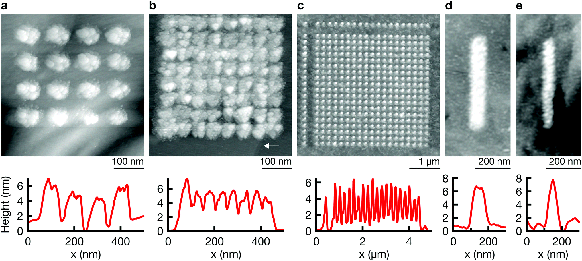 | ||
| Fig. 2 2D patterning. STM scans of patterns grown with a point-by-point strategy. Point-to-point spacing: (a) 100 nm, (b) 50 nm, (c) 200 nm, (d and e) 50 nm. The arrow in (b) points at two terrace edges of the (111) Au substrate—their visibility illustrates the strong confinement of the Co deposition. Deposition parameters. Electrolyte: 1 M (a–c), 0.5 M (d and e) CoSO4 in DMSO; pulse length: 100 ns; pulse amplitude: 6 V (a–c), 5 V (d and e); duty cycle: 0.01; pulses per point: 3000 (a–c), 2000 (d and e); dwell distance: 10 nm (a–d), 30 nm (e). | ||
Out-of-plane deposition
In general, more pulses per deposition event increase the height of the deposit (ESI Fig. S5†). Yet, the height of a dot grown upon a single deposition event, i.e., when firing a defined number of pulses while the tip is in its dwell position, must be smaller than the dwell distance. Otherwise, the deposit will short-circuit the tip and substrate, which usually results in large and poorly confined deposits. Hence, for a typical dwell distance of 10 nm and a lateral feature size of 50–100 nm, the maximum aspect ratio of a single deposit is 0.1–0.2. Building out-of-plane structures thus requires the sequential “stacking” of individual deposits. The respective procedure is outlined in Fig. 3a. After each dwell, the tip approaches the surface, detects the out-of-plane position of the grown deposit, and retracts by the defined dwell distance d. This routine maintains a constant spacing between tip and growing structure. The out-of-plane growth of the deposit can be tracked by recording the z-position of contact between tip and deposit. Graphs that plot this data are thus termed “growth curves”.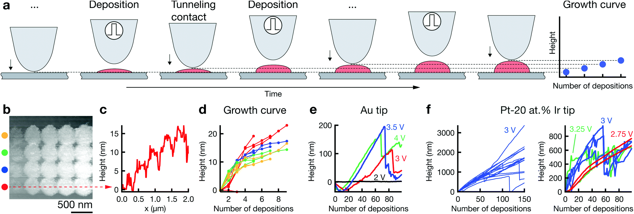 | ||
| Fig. 3 Towards 3D: out-of-plane growth. (a) Repetition of single deposition events at the same location enables sequential “stacking” of deposits. The growth of the deposit can be monitored in a "growth curve", recording the position of contact between tip and deposit during repositioning of the tip after each deposition event. (b) STM scan of a grid of dots deposited with an increasing number of consecutive deposition events per point in each row (left to right, from one to nine in steps of two). (c) Corresponding cross-section line profile of the bottom row. (d) Growth curves for each of the dots in (b). Colors correspond to the four rows in (b). (e) Growth curves for a larger number of deposition events as a function of pulse amplitude obtained with a Au tip. Note the absence of growth for a pulse amplitude of 2 V (black, no deposition) and the initial, negative values at higher pulse voltages indicating etching of the tip. (f) Growth curves recorded with a Pt-20 at% Ir tip in an aqueous electrolyte. Stable growth up to a height of 2–3 μm can be achieved (left), but growth curves are not free of instabilities. Curves recorded for pulse amplitudes of 2.75, 3 and 3.25 V (right) show that low amplitudes enable continuous growth, while larger pulse voltages cause growth instabilities. Deposition parameters. Electrolyte: 1 M CoSO4 in DMSO (b–e), 1 M aq. CoSO4 (f); pulse length: 100 ns (b–e), 20 ns (f); pulse amplitude: 4 V (b); duty cycle: 0.01; pulses per deposition event: 3000 (b–e), 10000–30000 (f); dwell distance: 10 nm (b–e), 50 nm (f); dwell time: 0.2 s (b–e), 0.5 s (f); tip: Au (b–e), Pt-20 at% Ir (f). | ||
Fig. 3b presents an array of dots deposited by increasing the number of deposition events from left to right. Note that the width of the deposits does not increase with height (except after the first deposition event). The corresponding cross-section line profile demonstrates the gradual increase in height of the individual dots (c), from approximately 5 nm (three deposition events, aspect ratio approximately 5 nm/400 nm = 0.01) to approximately 15 nm (nine deposition events, aspect ratio approximately 0.04). The same growth is also indicated by the corresponding growth curves in panel (d). Thus, out-of-plane growth is in principle accessible and can be tracked with the growth curves. Growth curves for larger numbers of consecutive deposits suggest an out-of-plane deposition rate of up to 5 nm s−1 in DMSO (Fig. 3e, 3.5 V) and 20 nm s−1 in water (Fig. 3f). Despite repeated efforts, we have been unable to image the grown structures by electron microscopy post deposition. Potentially, the structures grown by repeated deposition are fragile and washed away upon rinsing the substrate, or they are dissolved due to inaccurate potential control or loss thereof during rinsing. We can thus only speculate about the aspect ratios obtained in these experiments. The growth curves in Fig. 3f were recorded just after the experiments shown in Fig S9b,† using the same tip and deposition parameters. Let us thus assume that the width of the structures grown in Fig. 3f is the same as that of the deposits in Fig S9b,† approximately 200 nm (longer axis). The final aspect ratios of the structures in (f) would be 4–10, assuming there is no narrowing of the deposit's diameter as a function of height.
The irregular progress of growth indicates instabilities in the process (Fig. 3e). For a pulse amplitude of 2 V, no growth occurs. Increasing the pulse amplitude to 3–4 V results first in a dip of the growth curves to negative height values. Subsequently, the values typically increase, but are interrupted by sudden, pronounced drops. The initial drop is well explained by etching of Au tips, as described in ESI section 2.4† (note the steady surface detection at 2 V, indicating absence of tip crashes). After an initial incubation time, the out-of-plane growth rate of the deposit apparently outnumbers the etching rate, resulting in net positive values of the growth curve. The sudden drops in the growth curves are more difficult to assess. Recovery of growth after each drop speaks against a sudden and severe degradation of the tip, as this would likely cause termination of the experiment. We hypothesize that a shortcut between growing deposit and tip results in an instability of potential control and instantaneous dissolution of large parts of the grown deposit. Shortcuts were sometimes observed during application of pulses, presumably due to a contact of the growing deposit with the stationary tip. While we have not recorded the pulse current for these experiments, a shortcut caused by a deposit growing too fast could in principle be avoided by a continuous positioning feedback (during pulse off-time), and undesired swings in potential caused by a shortcut can be prevented by pausing potentiostat feedback during pulsing, as regularly employed in electrochemical machining.
Growth curves recorded for a Pt-20 at% Ir tip in aq. CoSO4 suggest an increased process stability compared to Au tips (Fig. 3f)—single deposits reach heights of 1–3 μm after 150 × 30000 pulses (3 V), and the number of growth curves that contain drops is decreased compared to experiments with Au tips. Nonetheless, abrupt collapses still occur with Pt-20 at% Ir tips. These instabilities seem to be a function of pulse amplitude. A pulse amplitude of 2.75 V results in continuous growth, while growth curves for higher voltages feature the previously observed drops. A comparison of pre- and post-deposition micrographs of the utilized tip's apex still indicates loss of material, as expected from the growth curves (ESI Fig. S10†). It is still to be shown that Pt or Pt-20 at% Ir tips do not degrade with appropriate process parameters.
What determines the feature size?
The resolution of electrochemical machining is generally well described by a model based on the one-dimensional charging time constant of the double layer.23,25,27 In our work, the qualitative influence of the machining parameters pulse length, electrolyte resistance, and dwell distance show the expected trends and corroborate importance of the general concept of local charging of the double layer (Fig. 4). Shortening pulse widths from 100 to 20 ns results in a decrease of the diameter of single Co deposits from ≈500 nm to ≈200 nm in an aqueous electrolyte (Fig. 4a), and from ≈150 nm to ≈50 nm in the DMSO electrolyte (Fig. 4b). Further, an increase in electrolyte resistance decreases the width of deposits. A comparison of Co dots deposited from 2 M aq. CoSO4 (ρ ≈ 20 Ω cm)28 and 1 M CoSO4 in DMSO (ρ ≈ 140 Ω cm)24 using 20 ns pulses reveals a decrease in diameter from ≈400 nm to ≈100 nm (long axis, Fig. 4c–e). Finally, an increased distance between tip and substrate results in a notable decrease of the lateral size of the deposits and a pronounced decrease of their volume (Fig. 4f and g). Coarsely optimizing all the mentioned factors resulted in the smallest features obtained up to date with our approach: the elliptical deposit in Fig. 4b (8 ns), with a FWHM of 25 and 58 nm for the short and long axis, respectively. Note that no tip deconvolution was performed. ESI Fig. S3† demonstrates reproducible reproduction of this smallest feature size in multiple experiments.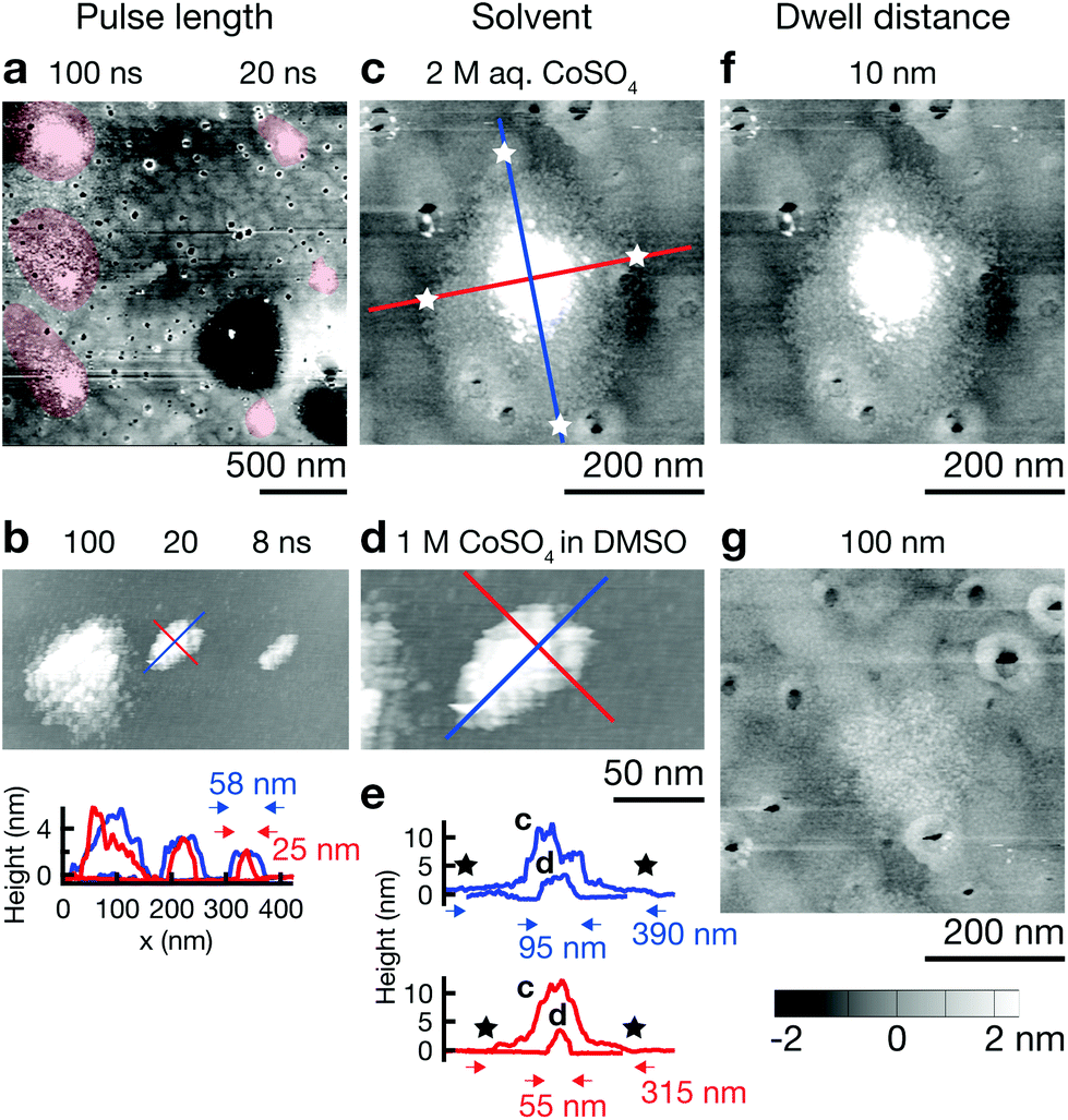 | ||
| Fig. 4 Parameters influencing the 2D feature size. The post-deposition STM scans compare the influence of a single parameter on the lateral extent of the deposit grown with otherwise unchanged parameters. (a and b) The longer the polarizing pulses, the larger the resulting deposits from aqueous electrolytes (a) as well as DMSO-based electrolytes (b). The areas of the deposits are shaded in red as a guide for the eye in (a). The line profiles in (b) indicate the width along the long (blue) and the short (red) axes of the ellipsoid deposits. (c–e) An increase in electrolyte resistance, i.e., when using DMSO (d) instead of water (c) as a solvent, increases the confinement for a given pulse length (20 ns, number of pulses: 500 (c), 50000 (d)): (e) plots cross-sections along the long (blue) and short (red) axes of the deposits. The width of the deposits was measured at their base. The stars highlight the extent of the deposit in (c). (f and g) The lateral size of the deposits decreases with dwell distance (e, 10 nm, f, 100 nm). The greyscale height scale applies to all STM scans. Deposition parameters. Electrolyte: 1 M CoSO4 in DMSO (b and d), 2 M aq. CoSO4 (a, c, f and g); pulse length: 20 ns (c–f); pulse amplitude: 5 V (a, c, f and g), 6 V (b and d); duty cycle: 0.01; pulses per point: 100 (a, 100 ns), 500 (a, 20 ns, c, f and g), 5000 (b, 100 ns) 50000 (b, 20 ns, d) 800000 (b, 8 ns); dwell distance: 10 nm (a, b, c, d and f), 100 nm (g). | ||
A quantitative comparison of the observed feature size of patterning shows that an approximation based on the 1D time constant of double layer charging significantly overestimates the deposit size, both in aqueous and DMSO electrolytes (by less than an order of magnitude though). For a specific electrolyte resistance of ρ ≈ 20 Ω cm (2 M aq. CoSO428) and ρ ≈ 140 Ω cm (1 M LiCl in DMSO,24 for a rough estimate of ρ of 1 M CoSO4 in DMSO), we estimate significant charging during a 20 ns pulse (τ = 20 ns) to a distance d = τ/(ρ × cDL) of ≈1 μm (water) and ≈150 nm (DMSO) (double layer capacitance of cDL = 10 μF cm−2). The expected diameter of a deposit would be approximately two times this value. In contrast, the approximate diameter of single Co deposits obtained with 20 ns pulses is 300–400 nm in water and 50–100 nm in DMSO (Fig. 4c and d) (typical tip radius of 50 nm, dwell distance of 10 nm). Note that unsatisfactory stability of the Au STM probes and thus a changing shape and size of the tip renders quantitative analysis of the present data questionable. Nonetheless we can state that the observed feature size is smaller than that predicted by the previous model because a blunting of the tip would lead to larger rather than smaller deposits. In further support of these observations, we report similar findings using more stable Pt tips in another publication.29
Thus, additional mechanisms of confinement must be at play. We hypothesize that the asymmetric electrode geometry and a significant nucleation overpotential caused by the short pulse time further limit the deposition in our favor. First, the 1D model of double layer charging assumes a parallel plate geometry and thus a ratio of area and capacitance of the two electrodes equal one—a given charge charges equal areas to equal potentials on both electrodes. This geometry closely represents the tool-substrate gap in micromachining and can be used to coarsely approximate the situation in the tip–substrate gap in our case. However, outside the tip–substrate gap, the ratio of tip area versus substrate area quickly becomes unfavourable for substrate charging—with increasing distance from the center, the rotational symmetry results in asymmetric charging of electrode areas connected by field lines, with the substrate being charged to a lower potential than the tip due to the ratio of surface area Asubstrate/Atip ≪ 1. In other words, the local overpotential on the substrate is actually smaller than that predicted by the simple 1D charging model which infers the local overpotential from the mere distance to the tip and ignores the ratio of surface area. Because of the expected exponential relationship of growth rate to local overpotential, local growth rate will rapidly decrease for a distance larger than one tip radius (≈50 nm) from the center of a deposit. Second, in contrast to etching, deposition requires the formation of nucleii of critical size during polarization time, necessitating the accumulation of a critical Co adatom concentration on the substrate during the pulse. Thus, we might very well expect that there is a minimum local deposition current to guarantee formation of stable nucleii during nanosecond pulse times, and that this current—an exponential function of the potential—is only met where highest overpotentials are reached in the center of the polarized zone. Thus, the nucleation barrier may effectively reduce the area that experiences charging sufficient for deposition and thus increase the resolution of the deposition method.
Where is the limit of attainable feature size then? We assume that a certain pulse width t charges the substrate to a potential UC sufficient for deposition within a distance d from the tip surface. With a spherical tip of radius r placed in front of a planar substrate, the width of the charged area then is described by 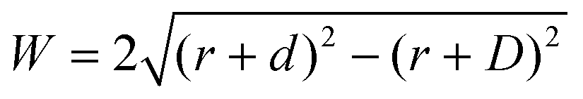 , with r the tip radius and D the dwell distance for W on the order of 2r (Fig. 5a), assuming a strictly radial current distribution in the electrolyte. Note that an important parameter, the pulse amplitude—directly affecting the local overpotential and thus, in our model, the charging distance d within which deposition occurs—is ignored in this simple model. Fig. 5b and c plots W as a function of d, D and tip radius r. W can be minimized by decreasing the tip radius and the charging distance d, or increasing the dwell distance D. Note that for any tip radius r, W becomes zero for d = D. This limit is unphysical, since for d → D the triangle in Fig. 5a becomes progressively acute and the lateral variation of the surface potential will ultimately vanish. However, from Fig. 5b it can be seen that for all tip radii the width of the structures will decrease with decreasing charging distance, that is, for shorter pulses. Yet, a significant reduction of pulse width will become technically and experimentally challenging to implement. Thus, an optimization of the dwell distance is an attractive alternative, because it can be experimentally realized with relative ease. Albeit our model will break down when the dwell distance reaches the charging distance, from Fig. 5c it can be seen that the width of the deposits strongly decreases with increasing dwell distance. We can coarsely predict a realistically achievable minimal feature size based on an experimentally verified charging distance d = 15 nm (assuming a simplified circular geometry for the smallest deposit achieved in Fig. 4b, a dwell distance of 10 nm and an approximate tip radius of 50 nm). Using d = 15 nm, let us place the tip at a realistic dwell distance of D = 12 nm < d. With a present tip radius of 50 nm, we could expect a width of 40 nm for the deposits. With a tip radius of 10 nm, obtainable with optimized etching procedures or FIB milling, the minimal feature size would drop to approximately 25 nm. Based on this prediction, a minimal feature size on the order of 10 nm—which would approach that of electron-beam-based techniques—seems realistic with further optimization of tip radius, dwell distance and pulse width.
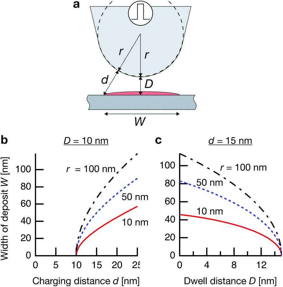 | ||
Fig. 5 Predicted width of a deposit. (a) Sketch of tip–substrate geometry. (b and c) Predicted width of deposits  (with tip radius r, dwell distance D, and distance from tip d, up to which the substrate is charged sufficiently for deposition during a pulse) as a function of (b), charging distance d (with D = 10 nm), and (c), dwell distance D (with d = 15 nm, which is experimentally observed in Fig. 4b). (with tip radius r, dwell distance D, and distance from tip d, up to which the substrate is charged sufficiently for deposition during a pulse) as a function of (b), charging distance d (with D = 10 nm), and (c), dwell distance D (with d = 15 nm, which is experimentally observed in Fig. 4b). | ||
General advantages and limitations of the concept
Confining substrate polarization during nanosecond voltage pulses is a robust approach for the strong localization of electrochemical reactions at the nanoscale (demonstrated herein for additive patterning, and previously for subtractive machining25,27). In combination with easily available nanometer sized probes, a minimal feature size of 10–50 nm is probably within reach. As the method is based on electrochemical reduction and utilizes precursors of high purity, one can expect a materials performance similar to that of other electrochemical methods.9 Thus, the concept could be attractive for niche applications that demand metals of high purity at smallest resolutions. A further advantage is the inherent growth feedback provided by all SPM based printing techniques—as shown in other work,14 such a feedback can enable controlled deposition of most complex geometries.Limitations of the concept are similar to those of other electrochemical techniques. First, a growth rate on the order of 10 nm s−1, i.e., 0.1 voxel per second for a typical feature size of 100 nm is comparable to deposition speeds of average FEBID and some electrochemical techniques,5 but low compared to up to 10 voxel per second for electrohydrodynamic redox printing4 (currently limited to a minimal feature size of about 100 nm) and tens and hundreds of voxel per second for non-electrochemical techniques5 (many of them with a minimal feature size of ≈1 μm). Note that the growth rate is currently slowed by a deposition procedure that is not optimized for speed, with significant delays added by the slow movement of the tip. For example, the summed pulse period time (pulse on and off time) for the 200 nm grown in 75 depositions in Fig. 3e was only 2.25 s, compared to 40 s needed to actually execute 75 depositions. Similarly, total pulse period time in Fig. 3f was 3 s versus a total process time of 150 s. Consequently, an increase in speed by a factor of ten is realistic for optimized deposition procedures that limit the movement of the tip and thus interruptions in the deposition process. For example, one could imagine a steady translation or retraction of the tip in combination with continuous pulsing. Yet, in contrast to the point-wise deposition strategy, a very limited number of experiments with continuous lateral translation of the tip at a fixed distance to the substrate and simultaneous polarization with nanosecond voltage pulses has not resulted in reproducible deposition up to this date. Potentially, the formation of new nuclei below the moving tip is hindered by ongoing growth of the initial deposit (which at this point in time is only at a small lateral distance from the tip) and consequent fast depolarization. More rigorous experimental work is needed to study this deposition mode, which could be attractive for higher deposition rates. Finally, an optimization of the low duty cycle required for deposition (0.01–0.1) and increased mass transport to re-supply the consumed ions in the tip–substrate gap could additionally increase deposition rate. For example, one can envision a combination of the method with concentration-confined electrodeposition14 which provides high rates of ion supply by pressure-dispensing a concentrated salt solution from a hollow AFM tip. A second limitation is the need for an electrically conductive substrate (although one can imagine wiring in-between electrodes, as shown for example with electrochemical electrohydrodynamic redox printing4). Finally, the application of the presented concept is easiest for electrochemical systems that are characterized by partly irreversible metal deposition—holding the surface potential between reduction and oxidation potentials separated by at least a few tens of mV avoids delocalized deposition but guarantees the stability of the localized deposits. We demonstrated growth of Co, but deposition of other metals, for example Ni, should be similarly feasible. To access a range of metals equal to that of other electrochemical methods (including reversible systems), the constraint towards irreversible electrochemical systems may be relaxed by careful control of the rest potentials of tip and surface, as demonstrated for local Cu deposition from acidic CuSO4 solutions.23
Conclusion
We have confirmed that confinement of electrodeposition by application of nanosecond voltage pulses to a local probe such as an STM tip can be used for reproducible 2D surface patterning with a feature size of <100 nm. As in electrochemical micromachining, the limited spatial extent of double-layer charging is the main mechanism to localize the electrochemical reaction, and pulse length and tip–substrate distance are the main parameters that control resolution. Yet, we assume that additional mechanisms based on the asymmetric tip–substrate geometry and a high nucleation barrier during short pulses further favor localization of deposition below the probe. We demonstrated a smallest feature size of about 50 nm (with the shorter axis of the elliptical deposit <50 nm) for Co deposition from a DMSO-based electrolyte with a tip radius of about 50 nm. With smaller tips, an optimized dwell distance during deposition and a moderate decrease of pulse width, a feature size on the order of 10 nm may be within reach, approaching values obtained with FEBID. Importantly, we identified issues with the stability of Au STM tips, and could demonstrate an enhanced inertness of Pt or Pt-20 at% Ir probes—a finding that will improve reproducibility in future experiments. The study highlights that the stability of the tip in a large process window is of utmost importance for the explored concept. Without an inert behavior of the probe, its size and shape and thus the size and shape of the deposits will not be constant, rendering reliable patterning and quantitative analysis of the deposition mechanism impossible. We have also demonstrated out-of-plane growth of Co structures, as evidenced by tracking their growth in situ. Notably though, we were unable to characterize the morphology of grown structures post deposition and future work is needed in this direction.In comparison with other electrochemical small-scale AM methods, the concept offers potential for smallest feature size, but currently a growth rate on the order of 0.1 voxel per second only. Further, we can conclude that there are still many technical challenges to the concept, but the instrumentation is simple compared to other methods that use complex, microfabricated probes or require ultra-high-vacuum equipment. Thus, the approach could succeed in niche applications that FEBID and other electrochemical strategies cannot serve, for example for applications that demand the site-specific deposition of smallest features of high purity, useful in nanophotonics30 (2D deposition on dielectrics, achieved with a sacrificial, nanometer-thin metal coating) or applications in field emission and sensing (3D deposition of out-of-plane nanowires).
Author contributions
AR wrote the control software and designed and built the STM-based deposition setup with support of R. Schuster. AR designed and performed experiments and their analysis. R. Spolenak advised AR's contribution to the work. AR drafted the manuscript, and all authors discussed the results and reviewed and commented on the text.Conflicts of interest
There are no conflicts to declare.Acknowledgements
The authors thank the members of the machine shop of the department of materials, ETH Zürich, for their contribution to the setup. AR would like to thank Marting Grüßer for his support of preliminary experiments at Karlsruhe Institute of Technology, Mark Aarts (AMOLF, Netherlands), who has conducted the experiments shown in Fig. 2d and e, as well as Steffen Geisel, Vladimir Vojtech and Johannes Gabl who evaluated various tip materials in their student projects. Electron-microscopy analysis was performed at ScopeM, the microscopy platform of ETH Zürich. The work was supported by ETH Zürich through grant No. ETH 47 14-2.References
- J. Sattelkow, J. E. Fröch, R. Winkler, S. Hummel, C. Schwalb and H. Plank, ACS Appl. Mater. Interfaces, 2019, 11, 22655–22667 CrossRef CAS PubMed.
- G. Arnold, R. Winkler, M. Stermitz, A. Orthacker, J. Noh, J. D. Fowlkes, G. Kothleitner, M. Huth, P. D. Rack and H. Plank, Adv. Funct. Mater., 2018, 28, 1707387 CrossRef.
- D. Kuhness, A. Gruber, R. Winkler, J. Sattelkow, H. Fitzek, I. Letofsky-Papst, G. Kothleitner and H. Plank, ACS Appl. Mater. Interfaces, 2021, 13, 1178–1191 CrossRef CAS PubMed.
- A. Reiser, M. Lindén, P. Rohner, A. Marchand, H. Galinski, A. S. Sologubenko, J. M. Wheeler, R. Zenobi, D. Poulikakos and R. Spolenak, Nat. Commun., 2019, 10, 1853 CrossRef PubMed.
- L. Hirt, A. Reiser, R. Spolenak and T. Zambelli, Adv. Mater., 2017, 201604211, 1604211 CrossRef PubMed.
- A. Botman, J. J. L. Mulders and C. W. Hagen, Nanotechnology, 2009, 20, 372001 CrossRef CAS PubMed.
- T. Lukasczyk, M. Schirmer, H.-P. Steinrück and H. Marbach, Small, 2008, 4, 841–846 CrossRef CAS PubMed.
- I. Utke, P. Hoffmann, B. Dwir, K. Leifer, E. Kapon and P. Doppelt, J. Vac. Sci. Technol., B: Microelectron. Nanometer Struct.–Process., Meas., Phenom., 2000, 18, 3168 CrossRef CAS.
- A. Reiser, L. Koch, K. A. Dunn, T. Matsuura, F. Iwata, O. Fogel, Z. Kotler, N. Zhou, K. Charipar, A. Piqué, P. Rohner, D. Poulikakos, S. Lee, S. K. Seol, I. Utke, C. Nisselroy, T. Zambelli, J. M. Wheeler and R. Spolenak, Adv. Funct. Mater., 2020, 30, 1910491 CrossRef CAS PubMed.
- P. Rohner, A. Reiser, F. T. Rabouw, A. S. Sologubenko, D. J. Norris, R. Spolenak and D. Poulikakos, Nanoscale, 2020, 12, 20158–20164 RSC.
- J. Schneider, P. Rohner, D. Thureja, M. Schmid, P. Galliker and D. Poulikakos, Adv. Funct. Mater., 2016, 26, 833–840 CrossRef CAS.
- M. A. Skylar-Scott, S. Gunasekaran and J. A. Lewis, Proc. Natl. Acad. Sci. U. S. A., 2016, 113, 6137–6142 CrossRef CAS PubMed.
- J. Hengsteler, B. Mandal, C. van Nisselroy, G. P. S. Lau, T. Schlotter, T. Zambelli and D. Momotenko, Nano Lett., 2021, 21, 9093–9101 CrossRef CAS PubMed.
- L. Hirt, S. Ihle, Z. Pan, L. Dorwling-Carter, A. Reiser, J. M. Wheeler, R. Spolenak, J. Vörös and T. Zambelli, Adv. Mater., 2016, 28, 2311–2315 CrossRef CAS PubMed.
- D. Momotenko, A. Page, M. Adobes-Vidal and P. R. Unwin, ACS Nano, 2016, 10, 8871–8878 CrossRef CAS PubMed.
- W. Schindler, D. Hofmann and J. Kirschner, J. Electrochem. Soc., 2001, 148, C124–C130 CrossRef CAS.
- R. Schuster, V. Kirchner, X. H. Xia, A. M. Bittner and G. Ertl, Phys. Rev. Lett., 1998, 80, 5599–5602 CrossRef CAS.
- B. W. Maynor, Y. Li and J. Liu, Langmuir, 2001, 17, 2575–2578 CrossRef CAS.
- C. Obermair, M. Kress, A. Wagner and T. Schimmel, Beilstein J. Nanotechnol., 2012, 3, 824–830 CrossRef PubMed.
- A. Jansson, G. Thornell and S. Johansson, J. Electrochem. Soc., 2000, 147, 1810 CrossRef CAS.
- W. Li, J. A. Virtanen and R. M. Penner, Appl. Phys. Lett., 1992, 60, 1181–1183 CrossRef CAS.
- J. R. LaGraff and A. A. Gewirth, J. Phys. Chem., 1995, 99, 10009–10018 CrossRef CAS.
- R. Schuster, V. Kirchner, P. Allongue and G. Ertl, Science, 2000, 289, 98–101 CrossRef CAS PubMed.
- X. Ma, A. Bán and R. Schuster, ChemPhysChem, 2010, 11, 616–621 CrossRef CAS PubMed.
- R. Schuster, ChemPhysChem, 2007, 8, 34–39 CrossRef CAS PubMed.
- O. de Abril, A. Gündel, F. Maroun, P. Allongue and R. Schuster, Nanotechnology, 2008, 19, 325301 CrossRef CAS PubMed.
- M. Kock, V. Kirchner and R. Schuster, Electrochim. Acta, 2003, 48, 3213–3219 CrossRef CAS.
- M. Bešter-Rogač, J. Chem. Eng. Data, 2008, 53, 1355–1359 CrossRef.
- M. Aarts, A. Reiser, R. Spolenak and E. Alarcon-llado, ChemRxiv, 2021.
- D. K. Gramotnev and S. I. Bozhevolnyi, Nat. Photonics, 2010, 4, 83–91 CrossRef CAS.
Footnotes |
| † Electronic supplementary information (ESI) available. See https://doi.org/10.1039/d1nr08409g |
| ‡ Present address: Department of Materials Science and Engineering, Massachusetts Institute of Technology, MA-02139 Cambridge, United States of America. |
| This journal is © The Royal Society of Chemistry 2022 |