DOI:
10.1039/D1NR08400C
(Paper)
Nanoscale, 2022,
14, 6425-6436
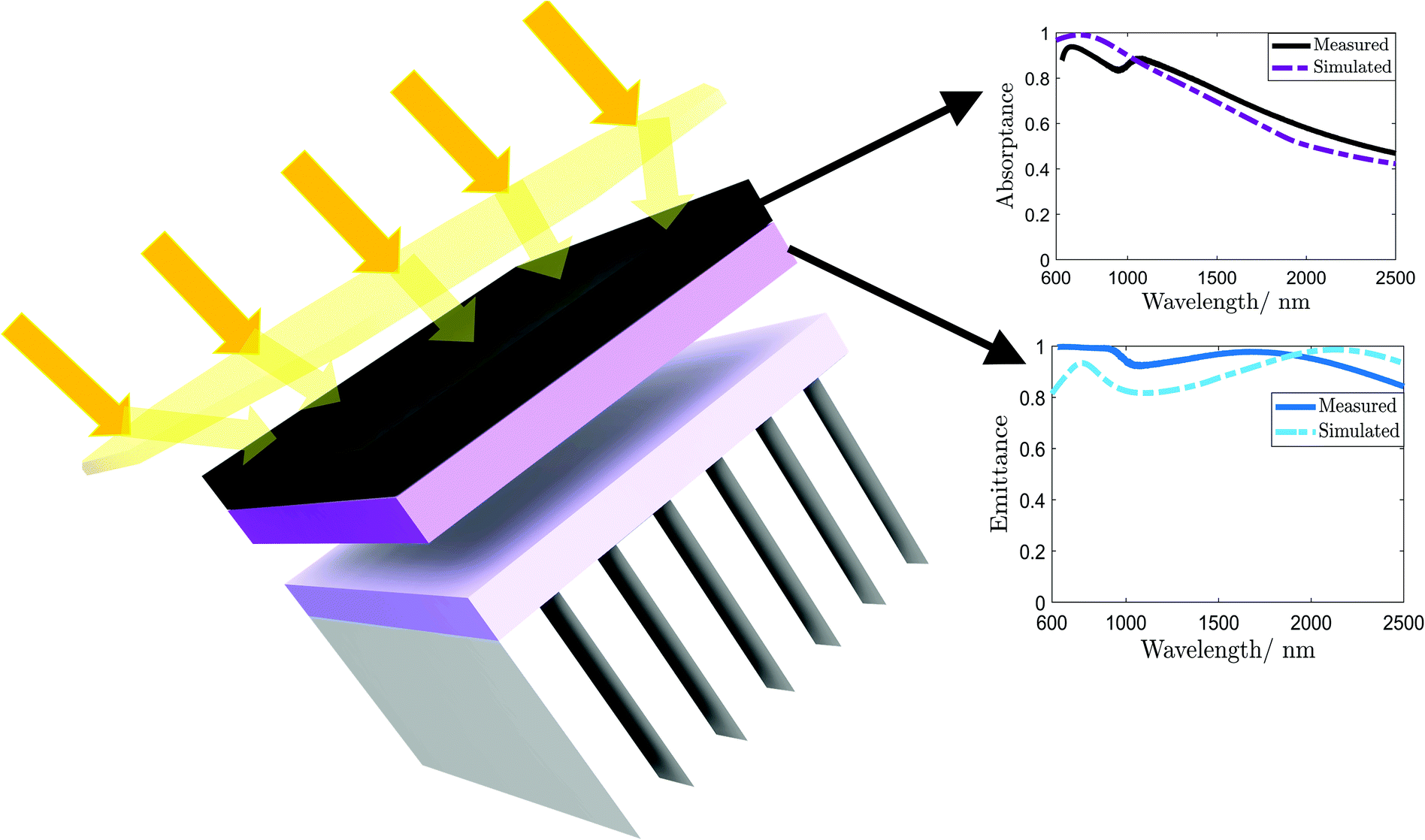
Nanostructured chromium-based broadband absorbers and emitters to realize thermally stable solar thermophotovoltaic systems
Received
22nd December 2021
, Accepted 27th March 2022
First published on 30th March 2022
Abstract
The efficiency of traditional solar cells is constrained due to the Shockley–Queisser limit, to circumvent this theoretical limit, the concept of solar thermophotovoltaics (STPVs) has been introduced. The typical design of an STPV system consists of a wideband absorber with its front side facing the sun. The back of this absorber is physically attached to the back of a selective emitter facing a low-bandgap photovoltaic (PV) cell. We demonstrate an STPV system consisting of a wideband absorber and emitter pair achieving a high absorptance of solar radiation within the range of 400–1500 nm (covering the visible and infrared regions), whereas the emitter achieves an emittance of >95% at a wavelength of 2.3 μm. This wavelength corresponds to the bandgap energy of InGaAsSb (0.54 eV), which is the targeted PV cell technology for our STPV system design. The material used for both the absorber and the emitter is chromium due to its high melting temperature of 2200 K. An absorber and emitter pair is also fabricated and the measured results are in agreement with the simulated results. The design achieves an overall solar-to-electrical simulated efficiency of 21% at a moderate temperature of 1573 K with a solar concentration of 3000 suns. Furthermore, an efficiency of 15% can be achieved at a low temperature of 873 K with a solar concentration of 500 suns. The designs are also insensitive to polarization and show negligible degradation in solar absorptance and thermal emittance with a change in the angle of incidence.
1 Introduction
On account of the growing population, urbanization, and industrialization, there is a constant escalation in the energy demand. Drawing power from the major sources of energy available today, i.e., coal, peat, and natural gas, has an adverse effect on the emission of greenhouse gases, e.g., CO2, CH4, and N2O that cause global warming. This leads to inevitable environmental degradation and climate change. Moreover, the limited reserves of these non-renewable resources also make them less suitable for use as they will run out in the near future. For the specific reasons of preserving natural resources and avoiding harmful greenhouse gas emissions, renewable energy sources are sought for power generation. The renewable energy source with the most potential in replacing all aforementioned resources is solar energy, which is provided by the sun at around 1 kW m−2 with no hazardous effect on the environment and is widely being used for various applications; electric power generation, solar thermal collectors for water heating, desalination, gasification etc. However, harnessing solar energy from the sun with a single junction silicon photovoltaic (PV) cell has a limitation of efficiency, as stipulated by Shockley in 1961.1 This efficiency can be enhanced by having multijunction PV cells or by the introduction of solar thermophotovoltaic (STPV) systems.
In 1979, Swanson2 coined the idea of solar thermophotovoltaics (STPV) to overcome the Shockley–Queisser limit, and this concept of the STPV system is shown in Fig. 1. The distinctive feature of STPV is the presence of an intermediate absorber/emitter pair, compared to the absence of an intermediate structure in traditional solar energy harvesting using PV cells. A solar absorber absorbs all the incoming radiation from the sun and converts it to thermal energy while a selective thermal emitter, which is physically connected to the absorber, emits thermal radiation of selective energy towards a low-bandgap photovoltaic (PV) cell. The emitter should be optimized for a PV cell in such a fashion that the emitted photons have energy slightly higher than the energy bandgap of the PV cell. This approach reduces the heat losses within the PV cell due to the absorption of high-energy photons, and therefore, can significantly enhance the solar conversion efficiency. The theoretical maximum efficiency of STPV systems can reach 85.4% at a temperature of 2544 K for the intermediate layer.3
 |
| | Fig. 1 Theoretical concept of STPVs with actual results from the proposed absorber/emitter designs. This figure is not made up to the proportion. | |
Over the last two decades, metasurfaces have found numerous applications in the domains of metaholograms,4–11,63 thin-flat lenses,12–14,64 chirality and dichroism,15–17 for harnessing of evanescent waves,18 structural color,19–22 and perfect light absorbers.23–28 Many researchers have proposed near unity absorbers and selective emitters made with metasurfaces individually, without combining these two into a unibody structure for STPV systems. In 2008, Nagpal et al.29 proposed a wideband absorber within the domain of 1–2.5 μm. Bonod et al.30 presented a structure based on lamellar metallic gratings for the absorption of light. Liu et al.31 in 2010 reported a narrowband absorber with a peak at a frequency of 185 THz for refractive index sensing. In 2011, Aydin et al.32 proposed visible light absorbers based on metallic gratings and trapezoid arrays with an average measured absorption of 0.71 within the visible spectrum. Wang et al.33 in 2015 employed nanostructured titanium gratings to obtain high absorption in the UV, visible, and near IR ranges. Minh Nguyen et al.34 in 2017 reported a plasmonic grating-based perfect absorber for the visible and near-infrared (IR) wavelengths. In 2018, Katrodiya et al.35 proposed an ultra-wideband absorber with up to 96% absorption in some bands. In 2020, Li et al.36 gave a design based on tungsten elliptical arrays with >90% absorption between 300–2200 nm. Qin et al.37 in 2020 also reported a perfect absorber with 99% absorption between 650–2200 nm. Some other report absorbers achieving high efficiency can also be found in the literature.38–42
From Kirchhoff's law, under thermodynamic equilibrium, absorptance is equal to emittance. In light of this law, researchers have also reported selective emitters for specific applications. Liu et al.43 in 2011 design metamaterial emitters with unity emittance for selective regions and near-zero emittance elsewhere. Mason et al.44 also reported the design of selective thermal emitters using gold strips of 3.2 μm and a periodicity of 4.8 μm at a temperature of 160 °C. Woolf et al.45 in 2018 demonstrated a TPV energy conversion mechanism using a metamaterial selective emitter with a thermal-to-electrical conversion efficiency of 24%.
Plentiful research has focused on individual absorber and emitter designs; however, limited research is available on the complete STPV system with an absorber/emitter pair having broadband absorption for the absorber and selective emittance for the emitter in the mid-infrared region, corresponding to the bandgap energy of the PV cell. Lenert et al.46 in 2014 proposed a carbon nanotube absorber and photonic crystal emitter pair with an experimental efficiency of just 3.2%. Rinnerbauer et al.47 proposed multi-walled carbon nanotubes (MWNTs) with an efficiency of 3.74%, at a solar concentration of 130 suns. Nam et al.48 in 2014 reported a 10% efficiency at a temperature of 1400 K with a flux of 130 kW m−2. In 2016, Bierman et al.49 reported a solar-to-electrical conversion efficiency of 6.8 (±) 2% that can be improved up to 10–15% if the PV cell used for the experiment is InGaAsSb with a bandgap of (0.54 eV); however, the efficiency is still far away from the ideal limit. Then in 2018, Chang et al.50 reported an efficiency of 18% at a solar concentration of 4000 suns at a temperature of 1380 °C using tungsten resonators. A few other reported STPV systems achieving good overall performance for both the absorber and emitter also exist in the literature.51–53
Apart from the solar to electrical conversion efficiency, which inherently requires polarization insensitivity and angular stability, nanostructured absorbers and emitters forming STPV systems also need thermal stability for better performance at high temperatures. For this purpose, metals with high melting points can be employed in the designs. However, metals suffer from a degradation factor of oxidation, which is also one of the primary obstacles in developing STPV systems. Based on all these requirements and conditions imposed for a high-efficiency STPV system, the absorber/emitter pair's design, optimization, and material selection become a challenging task.
In this work, we present a complete STPV system design, which demonstrates a solar-to-electrical conversion efficiency of 21%, at a temperature of 1573 K. These results are achieved at a solar concentration of 3000 suns, employing chrome nano-cylinder arrays for both the absorber and emitter structures. The design principles of nano-cylinder arrays are based on the mathematical model of the Cantor set. The melting point of chromium is around 2200 K, which is higher than the highest temperature needed by the proposed STPV system in order to achieve maximum efficiency. Moreover, chromium has an oxidation resistance capability due to the formation of a top Cr2O3 layer that prevents oxidation during its exposure to air making chromium highly oxidation-resistant. The designs are also polarization-insensitive and show minimal deviation in absorptance with a change in the angle of incidence. The designed Cantor set absorber achieves an absorptance of more than 90% within the region of 400–1200 nm after which it decays down to 70% at 1500 nm. The emitter for our proposed STPV system has been designed to present peak absorptance at a wavelength of 2.3 μm (0.54 eV), which corresponds to the energy bandgap of InGaAsSb.
2 Absorber design and efficiency
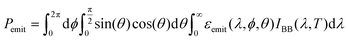
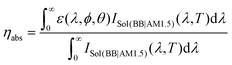
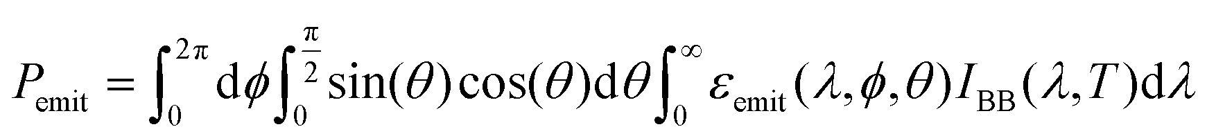
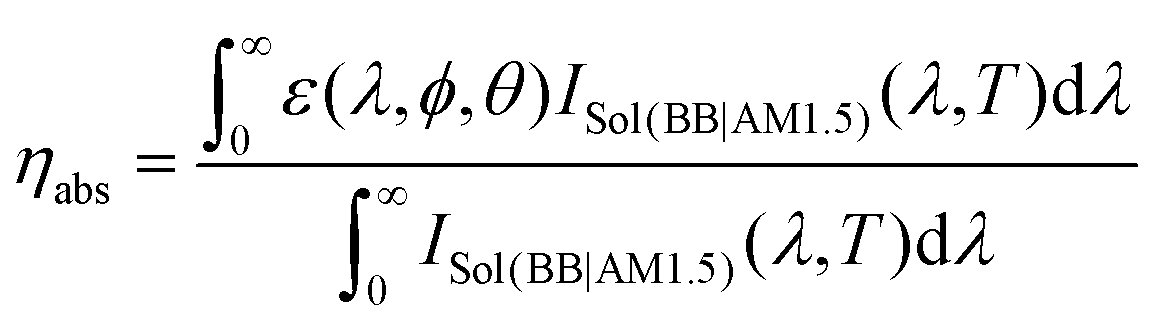
A perfect solar absorber for the STPV system should have an absorptance of 1 in the visible and near IR spectra while completely suppressing absorption at longer wavelengths to prevent the thermal emission from the absorber. Another key consideration while designing an absorber for an STPV system is its stability at high temperatures, which can be addressed by careful material selection. Moreover, for the STPV system design, it is assumed that every photon above bandgap will result in an electron–hole pair, the STPV system is placed in a vacuum chamber. Photon recycling is also ignored in the analysis. The key metric for the STPV absorber is α (absorptance of the absorber under a blackbody or AM 1.5 radiation spectra), which is defined by the following expression:54| |  | (1) |
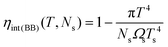
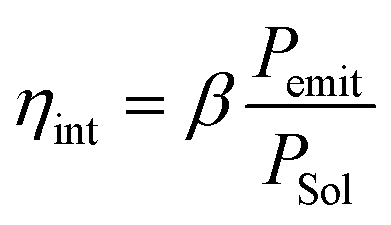
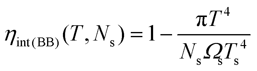
where ϕ is the polarization angle, θ represents the angle of incidence, ε is the emittance of the emitter, and λ is the wavelength. The system efficiency of an STPV is defined as:where ηint is the efficiency of the intermediate structure as shown in eqn (6).| |  | (3) |
| |  | (4) |
| |  | (5) |
| |  | (6) |
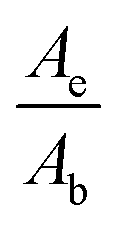
PSol is the solar irradiance, Pabs is the power absorbed by the absorber and Pemit is the thermal emission by the emitter at temperature T. At thermal equilibrium (for the intermediate structure involving an absorber and emitter pair), the incoming power is equal to the outgoing power. β is the ratio of the areas of the emitter and the absorber  , where Ae is the emitter area and Ab is the absorber area.
| | | PSol(Ns) − Pabs(T) = βPemit | (7) |
where Ns is the solar concentration of the sun. Therefore eqn (6) becomes.54| |  | (8) |
| |  | (9) |
where ϕ is the polarization angle, θ is the angle of incidence, and  , Ns is the solar concentration (number of suns), Ωs is the angle subtended by the sun, taken as 68.5 μSr, IBB(λ, T) is the intensity of radiation at the blackbody temperature, and Ts is the solar temperature taken as 6000 K.
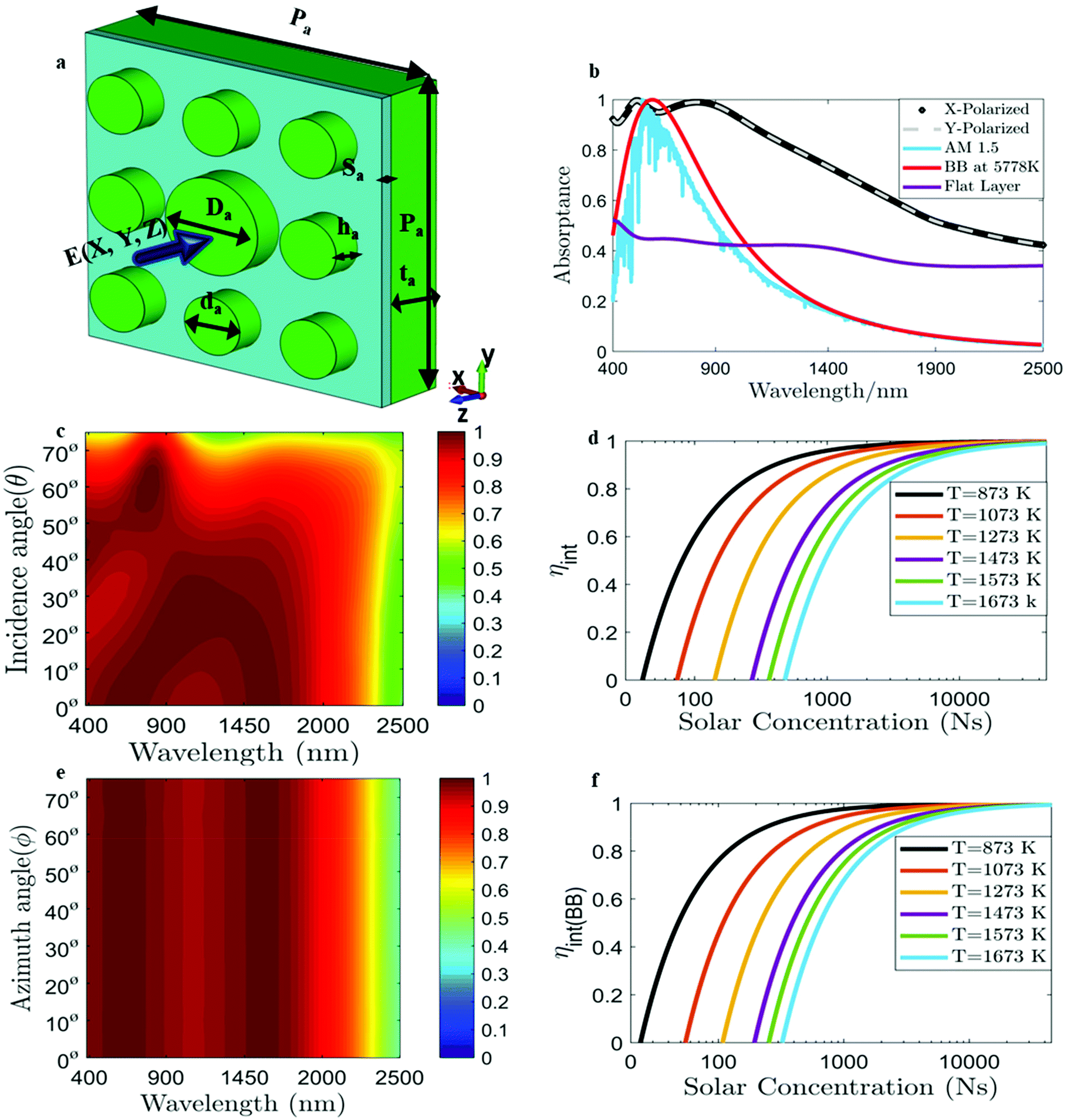
Based on the above requirements, we present a wideband absorber as shown in Fig. 2(a). The design consists of nine cylinders that are arranged in the form of a Cantor set, with a central cylinder of diameter Da, and surrounding cylinders of diameter da, deposited on a glass spacer with thickness Sa. The material used for the cylinders is chromium due to its high melting point of ∼2200 K, which makes the design robust to extreme temperatures. The design is based on a mathematical model of the Cantor set of order 2, nine cylinders of two different sizes are used. Each cylinder covers a specific absorption domain, which results in the overlapping of absorptance of all the nine cylinders, thereby creating a wide-band absorber covering the entire solar spectrum with an absorption of >0.8. Especially, within the spectrum range of 400–950, the absorption is as high as >0.95. The absorber efficiency is defined as the ratio of αopt to the total spectral blackbody radiation at 6000 K or AM 1.5.54
| |  | (10) |
 |
| | Fig. 2 (a) Perspective view of the unit cell of an absorber, ha = 70 nm; Da = 250 nm; da = 150 nm; ta = 150 nm; Sa = 30 nm; and Pa = 800 nm. (b) Absorption spectra of the designed absorber (black circles and dashed lines), as compared to those of a perfect blackbody at 6000 K (red), AM 1.5 (light blue), and a flat 70 nm chrome layer. (c) Change in the absorption spectra by changing the angle of incidence θ from 0 to 70°. (d) Intermediate efficiency of the absorber at different temperatures, with the solar concentration (Ns) on the x-axis on a logarithmic scale. (e) Change in the absorption spectra by changing the azimuth angle (ϕ) from 0° to 70°. (f) Intermediate efficiency of a blackbody absorber at different temperatures, with the solar concentration (Ns) on the x-axis on a logarithmic scale. | |
The absorptance of the presented structure is shown in Fig. 2(b) along with the absorption of an ideal blackbody at a temperature of 6000 K, and solar spectra with an air mass of AM 1.5, Fig. 2(b) also shows the comparison of the designed absorber with that of a flat chromium layer of thickness h. It can be noticed in the plot that it has an absorption of greater than 0.95 in the region of 400–1000 nm and then it starts decaying. At around 1500 nm the absorption goes down to 0.7, which further decays to 0.4 at a wavelength of 2300 nm. This absorption spectrum is desirable when considering that the ideal absorptance of the STPV absorber should be zero above the solar spectrum to prevent thermal radiation loss from the absorber. Moreover, the structure is insensitive to the incident wave polarization angle at normal (θ = 0), up to 70° as shown in Fig. 2(c). The results show that the absorption spectrum remains almost the same for different incidence angles of solar radiation, enhancing the overall efficiency of the system. The absorber efficiency of the presented structure is 89% for the blackbody radiation at 6000 K and 91% for AM 1.5. The full-wave electromagnetic solver CST Microwave Studio is used for performing numerical simulations55 and the wavelength dependent refractive index of chromium was taken from reported experimental data.56
The absorber should also be stable at high temperatures for reliable and high-efficiency use of the STPV, and also should be less sensitive to the polarization angles. The efficiency of the intermediate structure is shown in Fig. 2(d) as a function of solar concentration (Ns) at different structure temperatures. At low absorber/emitter temperatures, the proposed STPV system achieves a high intermediate efficiency as the solar concentration increases. However, the intermediate efficiency becomes lower at high absorber/emitter temperatures due to the thermal emission loss to the surroundings, suggesting that the solar concentration needs to be increased to achieve the maximum possible efficiency. In addition, the absorption curve remains almost identical to the change in the azimuth angle ϕ as shown in Fig. 2(e), which makes the design polarization-insensitive. At 873 K, the absorber achieves an intermediate efficiency of 92% at a low Ns value of 500 which is comparable to the state-of-the-art STPV absorbers operating at high temperatures. It can also be observed that if the solar concentration is kept constant, the intermediate efficiency decreases. As an example, if the temperature of the absorber is increased to 1573 K, at a solar concentration of 500 suns, ηint is reduced to 27.3%, in order to compensate we need to increase the solar concentration up to 2400 suns to achieve ηint of 85%. Similarly, at a temperature of 1673 K, an intermediate efficiency of 99% can be achieved at a high solar concentration of >40![[thin space (1/6-em)]](https://www.rsc.org/images/entities/char_2009.gif) 000 suns, so there is a trade-off between the high ηint and the solar concentration. Fig. 2(f) shows the intermediate efficiency plots in the case of a perfect blackbody absorber using eqn (9), and it can be seen that our proposed absorber works closely to the blackbody absorber by providing similar absorptance curves for various temperatures and solar concentrations.
000 suns, so there is a trade-off between the high ηint and the solar concentration. Fig. 2(f) shows the intermediate efficiency plots in the case of a perfect blackbody absorber using eqn (9), and it can be seen that our proposed absorber works closely to the blackbody absorber by providing similar absorptance curves for various temperatures and solar concentrations.
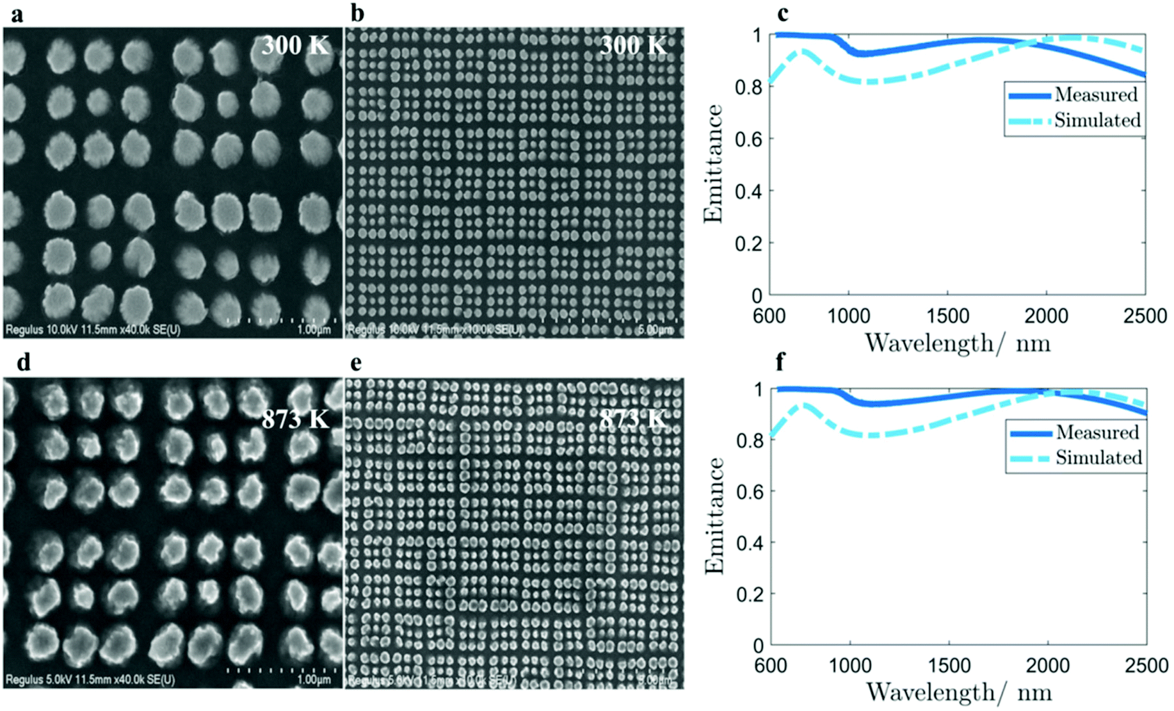
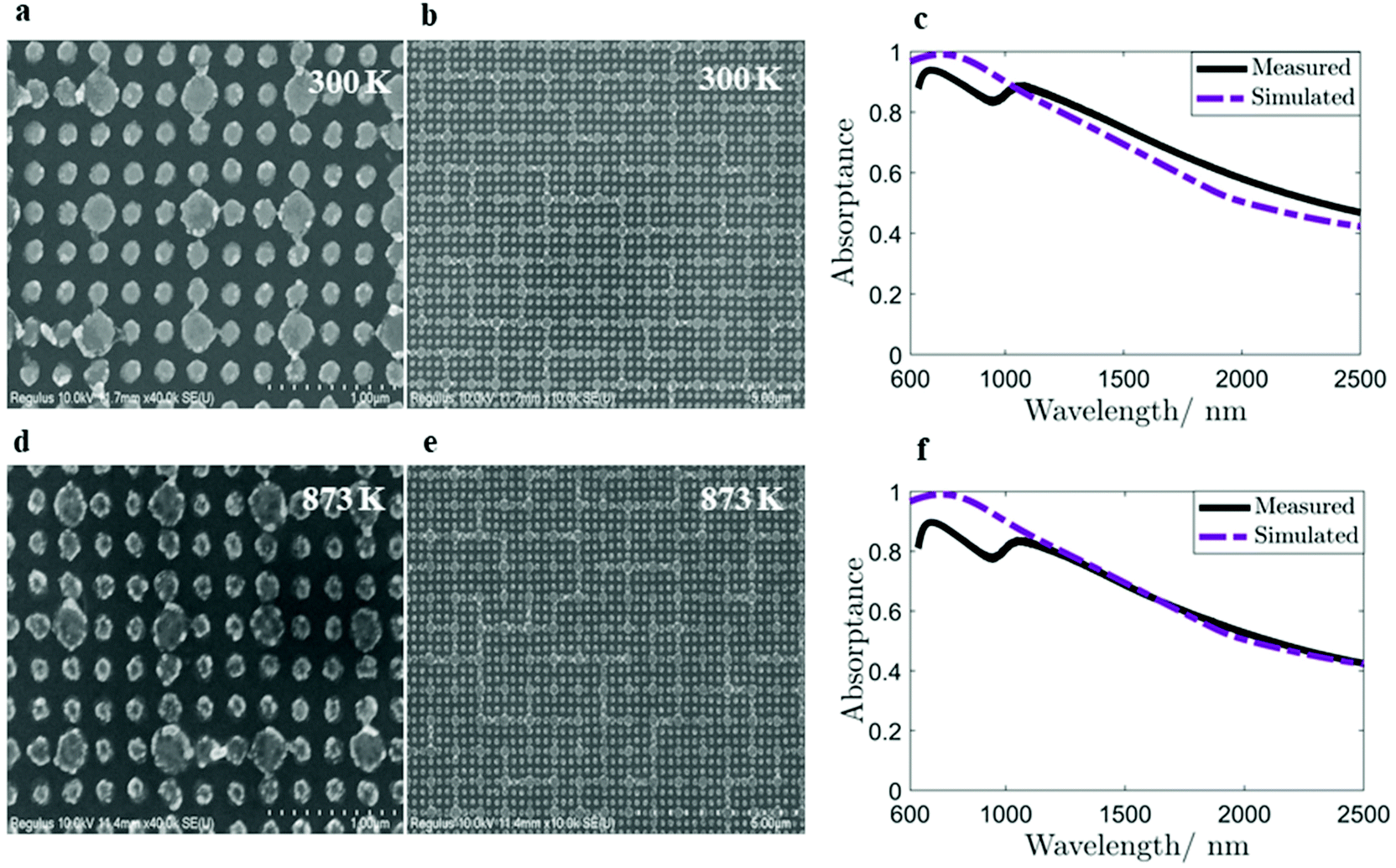
The SEM images of the design are provided in Fig. 3(a and b) at room temperature and in Fig. 3(d and e) at 873 K, respectively. Fig. 3(c) shows the measured absorptance of the fabricated absorber at 300 K, whereas Fig. 3(f) shows the measured absorption at a temperature of 873 K, and it can be seen that by increasing the temperature from 300 K to 873 K the proposed design retains its high absorptance.
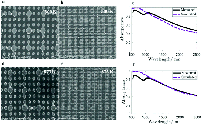 |
| | Fig. 3 SEM images of the absorber and the measured absorptance (a) at 300 K with a scale bar of 1 μm and (b) at 300 K with a scale bar of 5 μm. (c) Comparison of the measured and simulated emittances at 300 K, (d) at 873 K with a scale bar of 1 μm, and (e) at 873 K with a scale bar of 5 μm. (f) Comparison of the measured and simulated emittances at 873 K. | |
3 Emitter design and results
The function of the selective emitter is to emit thermal radiation towards the PV cell for thermophotovoltaic power generation. The emitter is physically attached to the absorber such that its front side faces the PV cell. Ideally, an emitter should have the highest emittance at the energy slightly above the energy bandgap of the PV cell, and elsewhere it should have no emittance at all. The PV cell for which we have optimized our STPV system is InGaAsSb which has the bandgap of 0.54 eV. This energy corresponds to a wavelength of 2.3 μm using the formula λ = hc/E. Since ε(λ,ϕ,θ) = α(λ,ϕ,θ) according to Kirchhoff's law, the design of the wavelength-selective emitter is similar to the broadband absorber, with the consideration of selective absorptance. The efficiency of an STPV system depends a lot on the selective behavior of the emitter and a high efficiency necessitates that an emitter should emit photons with energies that are slightly above the bandgap energy of the PV cell. However, the ideal emitter should not emit photons with above-bandgap energy to suppress the thermalization loss within the cell. Moreover zero-emission spectra below the bandgap of the PV cell is desirable because lower energy photons cannot generate electron–hole pairs.
Taking the emitter design rules into consideration, the proposed emitter structure is presented in Fig. 4(a) which is also based on the model of the Cantor set of order 2. The calculated spectral emittance is shown in Fig. 4(b), which has the emittance peak of 1 at 2300 nm in wavelength. Since we deal with energy while designing the emitter, the wavelength scale is converted into energy as shown in Fig. 4(d), along with the blackbody emission spectra at different temperatures. It can be seen in the figure that the emitter shows a very high emittance near the peak of the blackbody spectra for the temperatures of interest. The area ratio between the absorber and the emitter unit cells known as β is taken as 2.25.
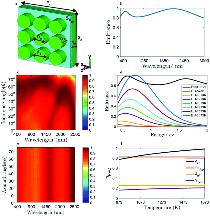 |
| | Fig. 4 (a) Perspective view of the unit cell of an emitter, he = 180 nm; De = 240 nm; de = 300 nm; te = 150 nm; Sa = 60 nm; and Pe = 1200 nm. (b) Emittance spectra of the designed emitter. (c) Change in the emittance spectra by changing the angle of incidence θ from 0° to 70°. (d) Emittance of the designed emitter plotted against the energy on the x-axis as compared to the normalized blackbody radiation spectra at different temperatures. (e) Change in the emittance spectra by changing the azimuth angle ϕ from 0° to 70°. (f) The efficiency of the emitter (ηPVC), Veff, ultimate efficiency (Ueff), and Im(Vop) at different temperatures. | |
The efficiency of the PV cell, ηPVC, solely depends on the emitter design as shown in the below equation:50
| | | ηPVC = Ueff·Veff·Im(Vop) | (11) |
where
Ueff is the ultimate efficiency of the solar cell, also known as the spectral conversion efficiency, and can be defined as:
| |  | (12) |
where
T is the temperature of the emitter, which in our case varies from 873 K to 1673 K. The value of
Ueff plays a central role in determining the efficiency of a PV cell, and this value depends on the emitted spectrum. The term
Eg/
E will approach unity for the energies slightly larger than the bandgap energy of the PV cell, then it would reduce monotonically for the larger values to make them less effective. Ideally, the emitter should be a narrow band such that it has an emittance of 1 at the bandgap energy to make the factor
Eg/
E nearly equal to 1, resulting in 100%
Ueff. The second term in
eqn (11) is the depreciation factor
Veff.
57| |  | (13) |
where
Kb is the Boltzmann constant,
Tc is the temperature at which the solar cell works, taken as 300 K,
q is the charge of an electron = 1.61 × 10
−19 C,
f is the non-ideality factor that is taken as 0.5 for planar geometries of the emitter and the PV cell, and
Vg =
Eg/
q. It should be noted that
Veff basically determines the ratio of above-bandgap photon energies emitted by the emitter to that emitted by the ideal emitter (having a narrowband absorptance just above the bandgap of the PV cell). The value of
Veff increases with an increase in the temperature of the emitter. The third term in the equation used for the efficiency calculation of the PVC is Im(
Vop), which can be calculated from the impedance matching.
57| |  | (14) |
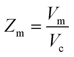
where

.
Zm is also related to

, where
Zop =
Zm + ln(1 +
Zm).
Using eqn (11), the PV cell efficiency (ηPVC) is estimated to be 21% at a temperature of 1573 K as shown in Fig. 4(f). We have designed the emitter keeping in mind the constraints for developing STPV systems which include stability at high temperatures, oxidation resistance (through material properties or addition of dielectric coatings), and also less complexity of them since it can create inefficiencies during the fabrication process. Most of these requirements are addressed by the material, chromium, which has a melting point of nearly 2200 K that is 527 K more than the 1673 K, the temperature at which the maximum efficiency from our design could be achieved. Fig. 4(c) and (e) show the angle insensitivity of the emitter. It can be observed that, like the absorber, the emitter also shows very little degradation by a change in the angle of incidence θ and the azimuth angle ϕ. In order to further enhance its thermal stability and inertness to oxidation, a thin layer of HfO2 is also coated on the structure. Fig. 5(a) and (b) show the SEM images of the fabricated sample at room temperature taken as 300 K. Fig. 5(c) shows the measured spectral emittance of the fabricated emitter at 300 K. Fig. 5(d) and (e) show the SEM images of the fabricated sample at 873 K. Fig. 5(f) shows the measured emittance at a temperature of 873 K. A comparison of these two figures reveals that the emittance increases by increasing the temperature from 300 K to 873 K.
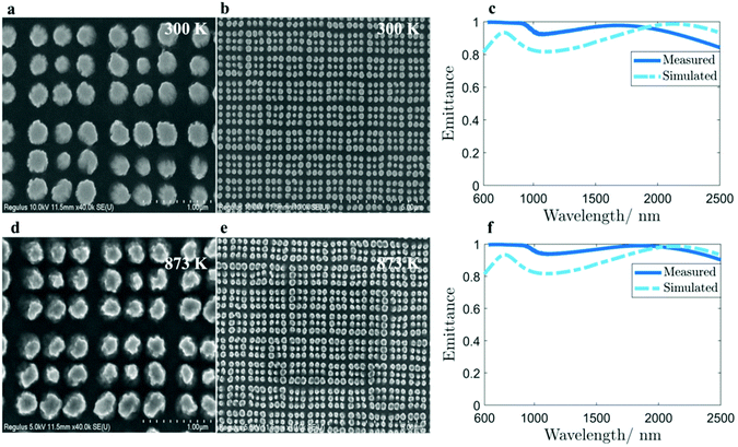 |
| | Fig. 5 SEM images of the emitter and the measured emittance (a) at 300 K with a scale bar of 1 μm and (b) at 300 K with a scale bar of 5 μm. (c) Comparison of the measured and simulated emittances at 300 K, (d) at 873 K with a scale bar of 1 μm, and (e) at 873 K with a scale bar of 5 μm. (f) Comparison of the measured and simulated emittances at 873 K. | |
4 System efficiency
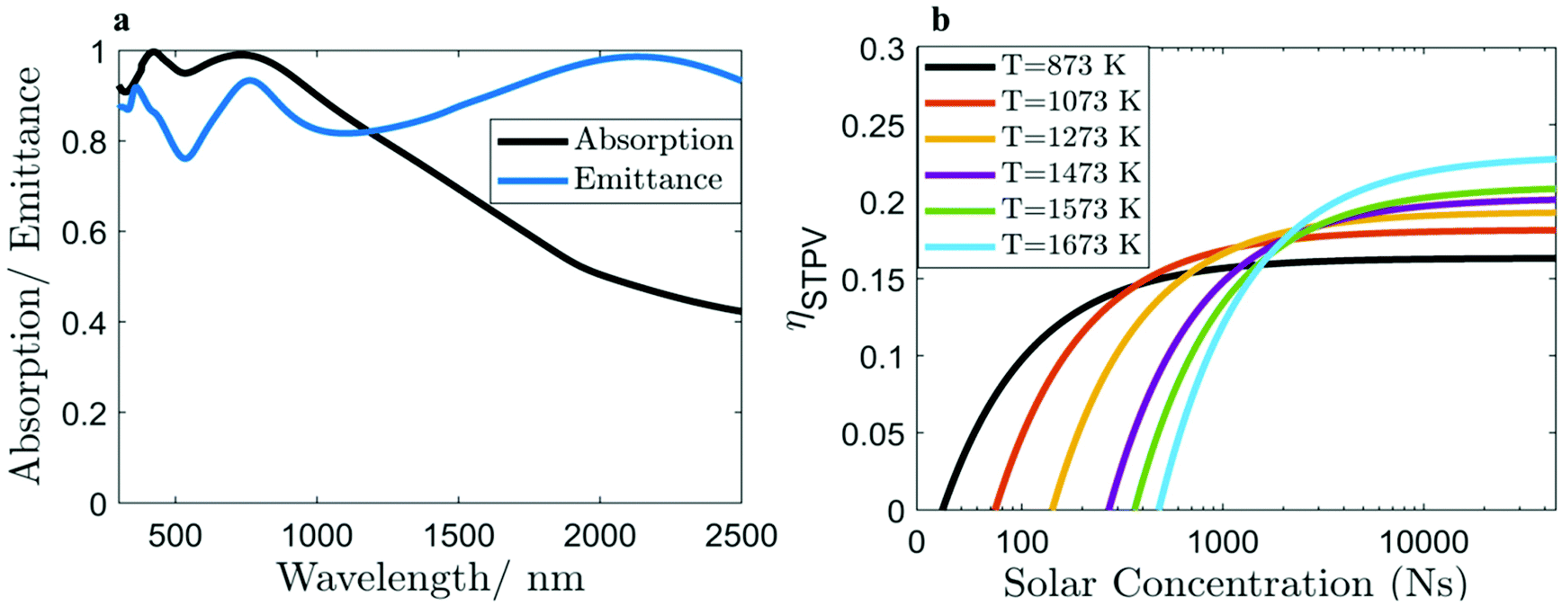
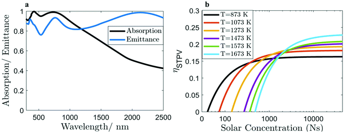
The efficiency of the whole STPV system depends on both the efficiencies of the absorber and emitter. An ideal absorber should absorb all the solar energy with an absorptance of 1, but at longer wavelengths (where blackbody radiation approaches zero) its absorption should be 0 so that it would not emit thermal radiation back to the surroundings. On the other hand, the emitter should emit radiation at a specific wavelength just shorter than the bandgap wavelength of the PV cell (which in our case is 2.3 μm for InGaAsSb). Eqn (2) was used for the calculation of the overall system efficiency and 16.5% ηPVC was observed in Fig. 4(d) at a low temperature of 1073 K at a solar concentration of 500 suns. To increase the efficiency of a system at a particular temperature we can increase the solar concentration (Ns). For the temperature of 1073 K, we can achieve an efficiency of 18.16% at a solar concentration of 4000 suns. Similarly, if we increase the temperature to 1273 K, the efficiency of the system can be enhanced to 18.5%, at a solar concentration of 1000 suns. However, in order to achieve an efficiency of greater than 21%, the temperature of the STPV should be 1673 K with a solar concentration of more than 5500 suns. In short, there is a trade-off between the maximum efficiency and the solar concentration, and high efficiency requires high solar concentration and temperature. In Fig. 6(a), combined plots of absorption and emittance are shown with the wavelength on the x-axis, and Fig. 6(b) shows the overall solar-to-electrical efficiency of the designed STPV at various temperatures. At a low temperature of 873 K, the solar-to-electrical efficiency of the STPV approaches approximately 15% at a solar concentration of 500 suns, similarly, at a temperature of 1073 K, the overall efficiency reaches 16% at a solar concentration of 1000 suns. This trend leads to >21% overall efficiency at 1673 K, at a high solar concentration of 5500 suns. The efficiency of the proposed STPV system, calculated from the absorptance curves of the fabricated samples, is comparable to the achieved efficiencies in contemporary STPV systems.46–53 Moreover, chromium metal, though it has the lowest melting point amongst refractory metals, presents exemplary characteristics of corrosion and oxidation resistance,58,59 which are crucial for STPV applications. These well-known properties of chromium result from the formation of a very thin coating of chromium dioxide (Cr2O3) on the surface60 when chromium is exposed to air (sometimes referred to as self-passivation of chromium), this mechanism prevents any further oxidation, making chromium highly oxidation-resistant. Therefore, the chromium-based designs presented here are better suited for operation under elevated temperature and pressure conditions, even in comparison to metals with a higher melting point having lower resistance to oxidation, such as tungsten.50,57 The only limiting factor of the presented STPV system is the lower selectivity of the emitter that yields lower ultimate efficiency (Ueff). This decrease in Ueff is also somewhat compensated by the simultaneous increase in Veff that increases with an increase in the broadband response of the emitter. To further increase the efficiency of the system, a different operating point can be selected, which requires a higher solar concentration. An example of the operating point comes at 1673 K with 40000 solar concentrations, where our design yields 24% overall efficiency.
 |
| | Fig. 6 (a) Absorption and emittance with respect to wavelengths. (b) Overall system efficiency with respect to the solar concentration (Ns) at different temperatures. | |
Both the absorptance and emittance were calculated from the measured reflectance using Fourier transform infrared spectroscopy (FTIR). Since there is no transmission, we calculated the absorptance and emittance by subtracting the measured reflectance from 1. The SEM images in Fig. 3(a, b, d, and e) and 5(a, b, d, and e) show some deviation from the original design, this is because patterning refractory metals is difficult. Therefore, both the absorber and emitter were fabricated by the Cr deposition and lift-off process. In the lift-off process, nanostructures can be tapered, and the roughness of the sidewall can be high. This can be improved by etching the Cr layer using a patterned photoresist (PR) as a etch mask. In this way, a negative PR should be used; however, the negative PR has a complicated lift-off process. Therefore, we fabricated the sample with the deposition/lift-off process. Similarly a change in the absorptance and emittance spectra at 873 K as compared to at 300 K can be seen in Fig. 3(f) and 5(f), respectively, is due to a change in the refractive index of Cr at high temperatures.61,62
5 Conclusion
A broadband absorber with an overall absorption of 89% along with an emitter is presented for an STPV system. The material used for both the absorber and the emitter is chromium owing to its thermal stability at high temperatures. The overall solar-to-electrical efficiency of the system comes out to 21% at a moderate temperature of 1573 K with a solar concentration of 3000 suns. An STPV efficiency of 15% is achieved at a low temperature of 873 K at a low solar concentration of 500 suns. Due to the symmetric structures of both the absorber and emitter designs, the design is completely polarization-insensitive as well as angle insensitive up to 70°, and hence the absorption spectra remain almost constant making the designs stable for a wide range of incidence angles. The 97% emittance of the selective emitter at a wavelength of 2300 nm, which corresponds to the bandgap energy of the InGaAsSb PV cell, plays a vital role in the efficiency enhancement of the system. The efficiency of the design is comparable to recent demonstrations of STPV systems; however, it is not the forte of our design. The significant benefit of the proposed design comes from the shape of intrinsic corrosion and oxidation resistance properties of chromium, which increases the stability of the STPV system.
Author contributions
M.A.A., J.K. and A.S.R. have contributed equally. M.Z., M.Q.M. and J.R. conceived the idea and initiated the project. M.A.A., A.S.R., B.R. and Z.A. designed the structure and performed the numerical simulations. J.K., I.K., J.S. and T.B. designed the process and experiments and fabricated the device. Y.M. and K.P. analysed the data. M.A.A. and A.S.R. mainly wrote the manuscript. J.R., M.Z. and M.Q.M. guided the entire research. All authors participated in discussion and have confirmed the final manuscript.
Conflicts of interest
The authors declare that there are no conflicts of interest.
Acknowledgements
This work was financially supported by the POSCO-POSTECH-RIST Convergence Research Center program funded by POSCO, and the National Research Foundation (NRF) grants (NRF-2019R1A2C3003129, CAMM-2019M3A6B3030637, NRF-2019R1A5A8080290, and NRF-2018M3D1A1058997) funded by the Ministry of Science and ICT (MSIT) of the Korean government. J.K. acknowledges the POSTECH Alchemist fellowship. I.K. acknowledges the NRF Sejong Science fellowship (NRF-2021R1C1C2004291) funded by the MSIT of the Korean government.
References
- W. Shockley and H. J. Queisser, Detailed balance limit of efficiency of p-n junction solar cells, J. Appl. Phys., 1961, 32(3), 510–519, DOI:10.1063/1.1736034.
- R. M. Swanson, A Proposed Thermophotovoltaic Solar Energy Conversion System, Proc. IEEE, 1979, 67(3), 446–447, DOI:10.1109/PROC.1979.11270.
- N. P. Harder and P. Würfel, Theoretical limits of thermophotovoltaic solar energy conversion, Semicond. Sci. Technol., 2003, 18(5), S151, DOI:10.1088/0268-1242/18/5/303.
- G. Yoon, D. Lee, K. T. Nam and J. Rho, Pragmatic Metasurface Hologram at Visible Wavelength: The Balance between Diffraction Efficiency and Fabrication Compatibility, ACS Photonics, 2018, 5(5), 1643–1647, DOI:10.1021/acsphotonics.7b01044.
- M. A. Ansari,
et al., A Spin-Encoded All-Dielectric Metahologram for Visible Light, Laser Photonics Rev., 2019, 13(5), 1900065, DOI:10.1002/lpor.201900065.
- I. Kim,
et al., Holographic metasurface gas sensors for instantaneous visual alarms, Sci. Adv., 2021, 7(15), eabe9943, DOI:10.1126/SCIADV.ABE9943.
- M. A. Naveed,
et al., Optical spin-symmetry breaking for high-efficiency directional helicity-multiplexed metaholograms, Microsyst. Nanoeng., 2021, 7, 5, DOI:10.1038/s41378-020-00226-x.
- J. Kim, Y. Yang, T. Badloe, I. Kim, G. Yoon and J. Rho, Geometric and physical configurations of meta-atoms for advanced metasurface holography, InfoMat, 2021, 3(7), 739–754, DOI:10.1002/inf2.12191.
- I. Kim,
et al., Pixelated bifunctional metasurface-driven dynamic vectorial holographic color prints for photonic security platform, Nat. Commun., 2021, 12, 3614, DOI:10.1038/s41467-021-23814-5.
- I. Kim,
et al., Dual-Band Operating Metaholograms with Heterogeneous Meta-Atoms in the Visible and Near-Infrared, Adv. Opt. Mater., 2021, 9(19), 2100609, DOI:10.1002/adom.202100609.
- B. Xiong,
et al., Realizing Colorful Holographic Mimicry by Metasurfaces, Adv. Mater., 2021, 33(21), 2005864, DOI:10.1002/adma.202005864.
- R. Jin,
et al., Experimental Demonstration of Multidimensional and Multifunctional Metalenses Based on Photonic Spin Hall Effect, ACS Photonics, 2020, 7(2), 512–518, DOI:10.1021/acsphotonics.9b01608.
- G. Yoon, K. Kim, D. Huh, H. Lee and J. Rho, Single-step manufacturing of hierarchical dielectric metalens in the visible, Nat. Commun., 2020, 11, 2268, DOI:10.1038/s41467-020-16136-5.
- G. Yoon, K. Kim, S. U. Kim, S. Han, H. Lee and J. Rho, Printable Nanocomposite Metalens for High-Contrast Near-Infrared Imaging, ACS Nano, 2021, 15(1), 698–706, DOI:10.1021/acsnano.0c06968.
- Z. Wang, H. Jia, K. Yao, W. Cai, H. Chen and Y. Liu, Circular Dichroism Metamirrors with Near-Perfect Extinction, ACS Photonics, 2016, 3(11), 2096–2101, DOI:10.1021/acsphotonics.6b00533.
- L. Kang,
et al., Preserving Spin States upon Reflection: Linear and Nonlinear Responses of a Chiral Meta-Mirror, Nano Lett., 2017, 17(11), 7102–7109, DOI:10.1021/acs.nanolett.7b03882.
- J. Kim,
et al., Chiroptical Metasurfaces: Principles, Classification, and Applications, Sensors, 2021, 21(13), 4381, DOI:10.3390/s21134381.
- L. Li, K. Yao, Z. Wang and Y. Liu, Harnessing Evanescent Waves by Bianisotropic Metasurfaces, Laser Photonics Rev., 2020, 14(12), 1900244, DOI:10.1002/lpor.201900244.
- J. Jang, T. Badloe, Y. Yang, T. Lee, J. Mun and J. Rho, Spectral modulation through the hybridization of Mie-scatterers and quasi-guided mode resonances: Realizing full and gradients of structural color, ACS Nano, 2020, 14(11), 15317–15326, DOI:10.1021/acsnano.0c05656.
- J. Jang,
et al., Self-Powered Humidity Sensor Using Chitosan-Based Plasmonic Metal–Hydrogel–Metal Filters, Adv. Opt. Mater., 2020, 8(9), 1901932, DOI:10.1002/adom.201901932.
- C. Jung,
et al., Near-zero reflection of all-dielectric structural coloration enabling polarization-sensitive optical encryption with enhanced switchability, Nanophotonics, 2021, 10(2), 919–926, DOI:10.1515/nanoph-2020-0440.
- T. Lee,
et al., Nearly Perfect Transmissive Subtractive Coloration through the Spectral Amplification of Mie Scattering and Lattice Resonance, ACS Appl. Mater. Interfaces, 2021, 13(22), 26299–26307, DOI:10.1021/acsami.1c03427.
- G. Yoon, S. So, M. Kim, J. Mun, R. Ma and J. Rho, Electrically tunable metasurface perfect absorber for infrared frequencies, Nano Converg., 2017, 4, 36, DOI:10.1186/s40580-017-0131-0.
- A. S. Rana, M. Q. Mehmood, H. Jeong, I. Kim and J. Rho, Tungsten-based Ultrathin Absorber for Visible Regime, Sci. Rep., 2018, 8, 2443, DOI:10.1038/s41598-018-20748-9.
- I. Kim, S. So, A. S. Rana, M. Q. Mehmood and J. Rho, Thermally robust ring-shaped chromium perfect absorber of visible light, Nanophotonics, 2018, 7(11), 1827–1833, DOI:10.1515/nanoph-2018-0095.
- A. J. Ollanik, I. O. Oguntoye, G. Z. Hartfield and M. D. Escarra, Highly Sensitive, Affordable, and Adaptable Refractive Index Sensing with Silicon-Based Dielectric Metasurfaces, Adv. Mater. Technol., 2019, 4(2), 1800567, DOI:10.1002/admt.201800567.
- M. A. Ansari,
et al., Engineering spin and antiferromagnetic resonances to realize an efficient direction-multiplexed visible meta-hologram, Nanoscale Horiz., 2020, 5(1), 57–64, 10.1039/c9nh00460b.
- M. A. Abbas,
et al., Engineering multimodal dielectric resonance of TiO2 based nanostructures for high-performance refractive index sensing applications, Opt. Express, 2020, 28(16), 23509, DOI:10.1364/oe.397431.
- P. Nagpal, S. E. Han, A. Stein and D. J. Norris, Efficient low-temperature thermophotovoltaic emitters from metallic photonic crystals, Nano Lett., 2008, 8(10), 3238–3243, DOI:10.1021/nl801571z.
- N. Bonod, G. Tayeb, D. Maystre, S. Enoch and E. Popov, Total absorption of light by lamellar metallic gratings, Opt. Express, 2008, 16(20), 15431, DOI:10.1364/oe.16.015431.
- N. Liu, M. Mesch, T. Weiss, M. Hentschel and H. Giessen, Infrared perfect absorber and its application as plasmonic sensor, Nano Lett., 2010, 10(7), 2342–2348, DOI:10.1021/nl9041033.
- K. Aydin, V. E. Ferry, R. M. Briggs and H. A. Atwater, Broadband polarization-independent resonant light absorption using ultrathin plasmonic super absorbers, Nat. Commun., 2011, 2, 517, DOI:10.1038/ncomms1528.
- H. Wang, V. Prasad Sivan, A. Mitchell, G. Rosengarten, P. Phelan and L. Wang, Highly efficient selective metamaterial absorber for high-temperature solar thermal energy harvesting, Sol. Energy Mater. Sol. Cells, 2015, 137, 235–242, DOI:10.1016/j.solmat.2015.02.019.
- D. M. Nguyen, D. Lee and J. Rho, Control of light absorbance using plasmonic grating based perfect absorber at visible and near-infrared wavelengths, Sci. Rep., 2017, 7, 2611, DOI:10.1038/s41598-017-02847-1.
- D. Katrodiya, C. Jani, V. Sorathiya and S. K. Patel, Metasurface based broadband solar absorber, Opt. Mater., 2019, 89, 34–41, DOI:10.1016/j.optmat.2018.12.057.
- J. Li,
et al., Broadband solar energy absorber based on monolayer molybdenum disulfide using tungsten elliptical arrays, Mater. Today Energy, 2020, 16, 100390, DOI:10.1016/j.mtener.2020.100390.
- F. Qin,
et al., Ultra-broadband and wide-angle perfect solar absorber based on TiN nanodisk and Ti thin film structure, Sol. Energy Mater. Sol. Cells, 2020, 211, 110535, DOI:10.1016/j.solmat.2020.110535.
- Z. Liu, G. Liu, Z. Huang, X. Liu and G. Fu, Ultra-broadband perfect solar absorber by an ultra-thin refractory titanium nitride meta-surface, Sol. Energy Mater. Sol. Cells, 2018, 179, 346–352, DOI:10.1016/j.solmat.2017.12.033.
- S. K. Patel, S. Charola, C. Jani, M. Ladumor, J. Parmar and T. Guo, Graphene-based highly efficient and broadband solar absorber, Opt. Mater., 2019, 96, 109330, DOI:10.1016/j.optmat.2019.109330.
- Z. Liu,
et al., Colloid templated semiconductor meta-surface for ultra-broadband solar energy absorber, Sol. Energy, 2020, 198, 194–201, DOI:10.1016/j.solener.2020.01.066.
- S. Charola, S. K. Patel, K. Dalsaniya, R. Jadeja, T. K. Nguyen and V. Dhasarathan, Numerical investigation of wideband L-shaped metasurface based solar absorber for visible and ultraviolet region, Physica B: Condens. Matter, 2021, 601, 412503, DOI:10.1016/j.physb.2020.412503.
- D. Lee,
et al., Multiple-patterning colloidal lithography-implemented scalable manufacturing of heat-tolerant titanium nitride broadband absorbers in the visible to near-infrared, Microsyst. Nanoeng., 2021, 7, 14, DOI:10.1038/s41378-020-00237-8.
- X. Liu, T. Tyler, T. Starr, A. F. Starr, N. M. Jokerst and W. J. Padilla, Taming the blackbody with infrared metamaterials as selective thermal emitters, Phys. Rev. Lett., 2011, 107(4), 045901, DOI:10.1103/PhysRevLett.107.045901.
- J. A. Mason, S. Smith and D. Wasserman, Strong absorption and selective thermal emission from a midinfrared metamaterial, Appl. Phys. Lett., 2011, 98(24), 15–18, DOI:10.1063/1.3600779.
- D. N. Woolf,
et al., High-efficiency thermophotovoltaic energy conversion enabled by a metamaterial selective emitter, Optica, 2018, 5(2), 213, DOI:10.1364/optica.5.000213.
- A. Lenert,
et al., A nanophotonic solar thermophotovoltaic device, Nat. Nanotechnol., 2014, 9, 126–130, DOI:10.1038/nnano.2013.286.
- V. Rinnerbauer,
et al., Metallic photonic crystal absorber-emitter for efficient spectral control in high-temperature solar thermophotovoltaics, Adv. Energy Mater., 2014, 4(12), 1400334, DOI:10.1002/aenm.201400334.
- Y. Nam,
et al., Solar thermophotovoltaic energy conversion systems with two-dimensional tantalum photonic crystal absorbers and emitters, Sol. Energy Mater. Sol. Cells, 2014, 122, 287–296, DOI:10.1016/j.solmat.2013.12.012.
- D. M. Bierman,
et al., Enhanced photovoltaic energy conversion using thermally based spectral shaping, Nat. Energy, 2016, 1, 16068, DOI:10.1038/nenergy.2016.68.
- C. C. Chang,
et al., Higherature Refractory Metasurfaces for Solar Thermophotovoltaic Energy Harvesting, Nano Lett., 2018, 18(12), 7665–7673, DOI:10.1021/acs.nanolett.8b03322.
- M. Shimizu, A. Kohiyama and H. Yugami, High-efficiency solar-thermophotovoltaic system equipped with a monolithic planar selective absorber/emitter, J. Photonics Energy, 2015, 5(1), 053099, DOI:10.1117/1.jpe.5.053099.
-
A. Kohiyama, M. Shimizu and H. Yugami, Solar-thermophotovoltaic systems using spectrally selective absorber/emitter based on metal-dielectric multilayer, Next Gener. Technol. Sol. Energy Convers. VII, 2016, vol. 9937, p. 993704. DOI:10.1117/12.2237672.
- H. Wang, J. Y. Chang, Y. Yang and L. Wang, Performance analysis of solar thermophotovoltaic conversion enhanced by selective metamaterial absorbers and emitters, Int. J. Heat Mass Transfer, 2016, 98, 788–798, DOI:10.1016/j.ijheatmasstransfer.2016.03.074.
- A. S. Rana, M. Zubair, A. Danner and M. Q. Mehmood, Revisiting tantalum based nanostructures for efficient harvesting of solar radiation in STPV systems, Nano Energy, 2021, 80, 105520, DOI:10.1016/j.nanoen.2020.105520.
-
C. S. Technology, CST STUDIO SUITE® 2016 specification, 2016, p. 28 Search PubMed.
- P. B. Johnson and R. W. Christy, Optical constants of transition metals, Phys. Rev. B: Solid State, 1974, 9(12), 5056–5070 CrossRef CAS.
- E. Rephaeli and S. Fan, Absorber and emitter for solar thermo-photovoltaic systems to achieve efficiency exceeding the Shockley-Queisser limit, Opt. Express, 2009, 17(17), 15145, DOI:10.1364/oe.17.015145.
-
J. W. Fergus, High Temperature Corrosion of Intermetallic Alloys, Shreir's Corros, 2010, pp. 646–667. DOI:10.1016/B978-044452787-5.00078-0.
-
W. M. Garrison and M. O. H. Amuda, Stainless Steels: Martensitic, Ref. Modul. Mater. Sci. Mater. Eng, 2017. DOI:10.1016/B978-0-12-803581-8.02527-3.
- R. Mitra, Oxidation and environmental degradation of intermetallic matrix composites, Intermet. Matrix Compos., 2018, 321–358, DOI:10.1016/B978-0-85709-346-2.00012-1.
- M. F. Al-Kuhaili and S. M. A. Durrani, Optical properties of chromium oxide thin films deposited by electron-beam evaporation, Opt. Mater., 2007, 29(6), 709–713, DOI:10.1016/j.optmat.2005.11.020.
- A. B. C. Ekwealor, Variations of optical and structural properties with temperature for CrxOy thin films synthesized in a polymer matrix by chemical bath deposition technique, Dig. J. Nanomater. Biostructures, 2014, 9(1), 423–431 Search PubMed.
- J. Kim, D. Jeon, J. Seong, T. Badloe, N. Jeon, G. Kim, J. Kim, S. Baek, J.-L. Lee and J. Rho, Photonic Encryption Platform via Dual-Band Vectorial Metaholograms in the Ultraviolet and Visible., ACS Nano, 2022, 16(3), 3546–3553, DOI:10.1021/acsnano.1c10100 , 35184548.
- Dasol Lee,
et al. Hyperbolic metamaterials: fusing artificial structures to natural 2D materials, eLight, 2022, 2, 1, DOI:10.1186/s43593-021-00008-6.
Footnote |
| † Theses authors contributed equally to this work. |
|
| This journal is © The Royal Society of Chemistry 2022 |
Click here to see how this site uses Cookies. View our privacy policy here. 
 f,
Zubair
Ahmad
f,
Zubair
Ahmad

 , where Ae is the emitter area and Ab is the absorber area.
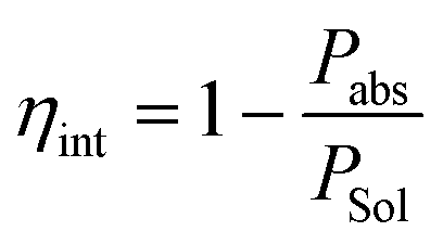
 , Ns is the solar concentration (number of suns), Ωs is the angle subtended by the sun, taken as 68.5 μSr, IBB(λ, T) is the intensity of radiation at the blackbody temperature, and Ts is the solar temperature taken as 6000 K.

 . Zm is also related to
 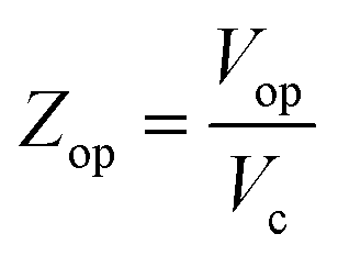 , where Zop = Zm + ln(1 + Zm).