
Application of patterned sapphire substrate for III-nitride light-emitting diodes
Shengjun
Zhou†
 *a,
Xiaoyu
Zhao†
a,
Peng
Du
a,
Ziqi
Zhang
a,
Xu
Liu
a,
Sheng
Liu
*b and
L. Jay
Guo
*c
*a,
Xiaoyu
Zhao†
a,
Peng
Du
a,
Ziqi
Zhang
a,
Xu
Liu
a,
Sheng
Liu
*b and
L. Jay
Guo
*c
aCenter for Photonics and Semiconductors, School of Power and Mechanical Engineering, Wuhan University, Wuhan 430072, China. E-mail: zhousj@whu.edu.cn
bThe Institute of Technological Sciences, Wuhan University, Wuhan, 430072, China. E-mail: victor_liu63@vip.126.com
cDepartment of Electrical Engineering and Computer Science, University of Michigan, Ann Arbor, MI 48109, USA. E-mail: guo@umich.edu
First published on 17th March 2022
Abstract
Recent decades have witnessed flourishing prosperity of III-nitride emitters in solid-state lighting and high-resolution displays. As one of the widely used substrates, sapphire shows superiority for heteroepitaxial growth of III-nitride light-emitting diode (LED) structure, due to the advantages of stability, low cost, high mechanical strength, as well as mature fabrication technology. However, realization of efficient LEDs grown on sapphire substrate is impeded by high density of defects in epilayers and low light extraction efficiency. The emergence of patterned sapphire substrate (PSS) turns out to be a promising and effective technology to overcome these problems and enhance the LED performances. In this review, we first introduce the background and recent advances of PSS applied in III-nitride visible and ultraviolet LEDs are. Then, we summarize the fabrication methods of PSS, together with novel methods to define nanometre-scale patterned structures. We further demonstrate the effect of PSS that contributes to reduce the threading dislocation density (TDD) of epilayers in detail. Meanwhile, mechanism of light extraction efficiency enhancement by adopting PSS is presented based on numerical analysis. Next, we explore the influence of PSS structural parameters (e.g. pattern size, pattern shape and aspect ratio) on LED performances, spanning from visible to deep ultraviolet UV emission region. Finally, challenges and potential prospects in PSS for future LED development are proposed and forecasted as well.
 Shengjun Zhou | Prof. Shengjun Zhou is a Professor at School of Power and Mechanical Engineering, Wuhan University. He received his Ph.D. degree from Shanghai Jiao Tong University in 2011. From 2014–2015, he was a research fellow at University of Michigan, Ann Arbor. His research interests focus on the growth and device fabrication of GaN-based LEDs. He has authored over 83 publications in peer-reviewed journals and conference proceedings. |
 Xiaoyu Zhao | Xiaoyu Zhao received his M.S. degree in 2020 from Institute of Semiconductor, University of Chinese Academy of Sciences. He is now a Ph.D. candidate at School of Power and Mechanical Engineering, Wuhan University. His research interests focus on the development of high-efficiency long-wavelength LEDs. |
 Peng Du | Peng Du received his B.S. degree in 2020 from Wuhan University. He is currently pursuing the master's degree with the School of Power and Mechanical Engineering, Wuhan University. His research interests focus on the simulation, fabrication, and design for AlGaN-based deep ultraviolet LEDs. |
 Ziqi Zhang | Ziqi Zhang received his M.S. degree in 2021 from Shandong University. He is currently a Ph.D. candidate at School of Power and Mechanical Engineering, Wuhan University. His research interests focus on the fabrication of high-efficiency LEDs. |
 Sheng Liu | Prof. Sheng Liu received his B.S. degree from Nanjing University of Aeronautics and Astronautics, China in 1983, and Ph.D. degree from Stanford University, USA in 1992. He is currently a professor at the School of Power and Mechanical Engineering, Wuhan University, with joint appointment at the Institute of Technological Science. His current research interests focus on the areas of LEDs, MEMS, optoelectronics, sensor and electronics packaging. He has authored or co-authored more than 300 publications in peer-reviewed journals and conference proceedings. He is a Fellow of IEEE and a Fellow of ASME. He serves on the Editorial Board of Science Bulletin and Microsystems & Nanoengineering. |
 L. Jay Guo | L. Jay Guo is a Professor at the University of Michigan, Ann Arbor. Prof. Guo's research covers polymer-based photonic devices and sensor applications, flexible transparent conductors, nanophotonics, hybrid photovoltaics and photodetectors, to nanomanufacturing technologies, and are contributed by students from Electrical Engineering and Optics, Macromolecular Science & Engineering, Applied Physics, and Mechanical Engineering. He has over 270 journal publications, and a H-index of 80 (by google scholar). He recently completed his Associate Editorship of Optica and currently an Associate Editor of IEEE J. Photovoltaics, and serves on the Editorial Advisory Board of Advanced Optical Materials. |
1. Introduction
Thanks to the crucial breakthroughs in epitaxially grown III-nitride materials for optoelectronic devices, great progress in LED technology has revolutionized the lighting industry globally.1–5 These materials, with tuneable band gap, are of considerable interest for light emission from deep ultraviolet (DUV) for AlN to near ultraviolet (NUV) for GaN, and to infrared for InN, showing great potential in wide range of applications.6–12 For instance, white LEDs combining blue or UV LEDs with wavelength-converting phosphors have great advantages over traditional incandescent and fluorescent lighting sources by providing lower energy consumption, longer lifetime, higher brightness, and environmental sustainability.13–15 Integration of red, green and blue (RGB) micro-LEDs has been highlighted not only for high color rendition white illumination, but for full-color displays, wearable devices, high-brightness augmented-reality (AR) and visual reality devices.16–19 Recently, III-nitride micro-LEDs play an important role in the biomedical area, due to its outstanding biocompatibility, low heating property and stability.20,21 Moreover, there has been unprecedented development of UV-LEDs due to potential applications in UV sensing, optical data storage, sterilization.22–26Nowadays, metal–organic chemical vapor deposition (MOCVD), molecular beam epitaxy (MBE) and hydride vapor phase epitaxy (HVPE) are commonly implemented methods for the epitaxial growth of LED structures.27–32 Relying on the substrate used and the material grown, epitaxial growth can be categorized as homoepitaxial and heteroepitaxial growth. Nevertheless, the former is hindered by the high cost of large-scale single crystals as substrates despite obtaining high-quality films.33 Heteroepitaxial growth on foreign substrate, such as sapphire, silicon and silicon carbide,34–37 is commercially available with a large market. Among them, sapphire has attracted much attention not only for its low cost, but various sizes, optical transmittance, excellent physical and chemical stability as well. However, LEDs grown on c-plane sapphire substrate suffer from high density of defects in epilayers, which arises from the large mismatch of lattice constant and thermal expansion coefficient between sapphire and GaN, degrading external quantum efficiency (EQE) and further device performance.28 Besides, EQE of LEDs is also related to light-extraction efficiency (LEE). Because of the considerable refractive index difference between epitaxial structure and air, only a few photons could transmit outside, while a large number of photons are trapped inside the epitaxial structure.38 These trapped photons are reabsorbed and eventually transformed to heat, accelerating the device degradation. To tackle these problems, patterned sapphire substrate (PSS) technology, which features artificial structures,29,39,40 has attracted great attention and achieved tremendous progress owing to its superiority over flat sapphire substrate (FSS) in several aspects.
(1) Patterns on PSS can be designed and fabricated with different structural parameters.
(2) Unlike normal ELO technique, there is no additional growth interruption during the growth process on PSS.
(3) PSS is a versatile platform applicable for growth of visible and UV LED structures.
(4) PSS effectively reduces the density of threading dislocation in epilayers, resulting in an increased internal quantum efficiency (IQE).
(5) PSS enhances the LEE by increasing the probability of light scattering, reducing light trapping in the LED.
Besides the aforementioned advantages, the roles of strain relaxation and suppression of quantum-confined Stark effect (QCSE) are also reported for PSS.41 Nowadays, benefiting from PSS, excellent achievements have been made from visible III-nitride LEDs to UV LEDs: EQE of blue LED increases to 84.3% and correspondingly fabricated white LED has a high luminous efficacy of 249 lm W−1 at an injection current of 20 mA.13 Blue micro-LED grown on PSS sustains a high EQE above 40% even on the ultrasmall scale (0.01 mm2)42 and red micro-LED exhibits high light output power density of 1.76 mW mm−2 at 50 A cm−2.43 As for UV LED, threading dislocation density (TDD) was reduced by approximately 50% and LEE was enhanced by 6.8% when PSS was further replaced by patterned sapphire with silica array, thereby leading to increment of 23.4% in EQE.24
As remarkable breakthroughs have been achieved in this field, there lacks a systematic review of the subject, which inspires this review (Fig. 1). We first introduce the recent advancements of PSS used for LEDs with emphasis on its advantage. Then, we present normal procedures and main methods of PSS fabrication together with emerging techniques. Next, we provide a detailed discussion of mechanisms that PSS enables the reduction of dislocation density in epilayers and the enhancement of LEE both for visible and UV LEDs. Afterwards, PSSs with different structure parameters and their influence on LED performance are presented. Finally, we discuss the challenges on the present stage and put forward the future directions of the PSS technology for efficient and high-performance LEDs.
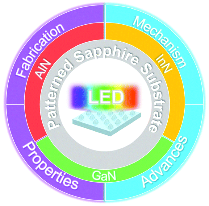 | ||
| Fig. 1 Application of patterned sapphire substrate for III-nitride light-emitting diodes. | ||
2. Fabrication methods
With the development of PSS, fabrication methods of PSS have become critical issues. In this section, the related fabrication methods including etching processes and pattern transfer techniques for micrometre-scale and nanometre-scale patterns are introduced.2.1 Etching methods
Fig. 2a shows the commonly used fabrication process for PSS, in which dry etching and wet etching are the main methods to transfer the pattern of mask onto the sapphire.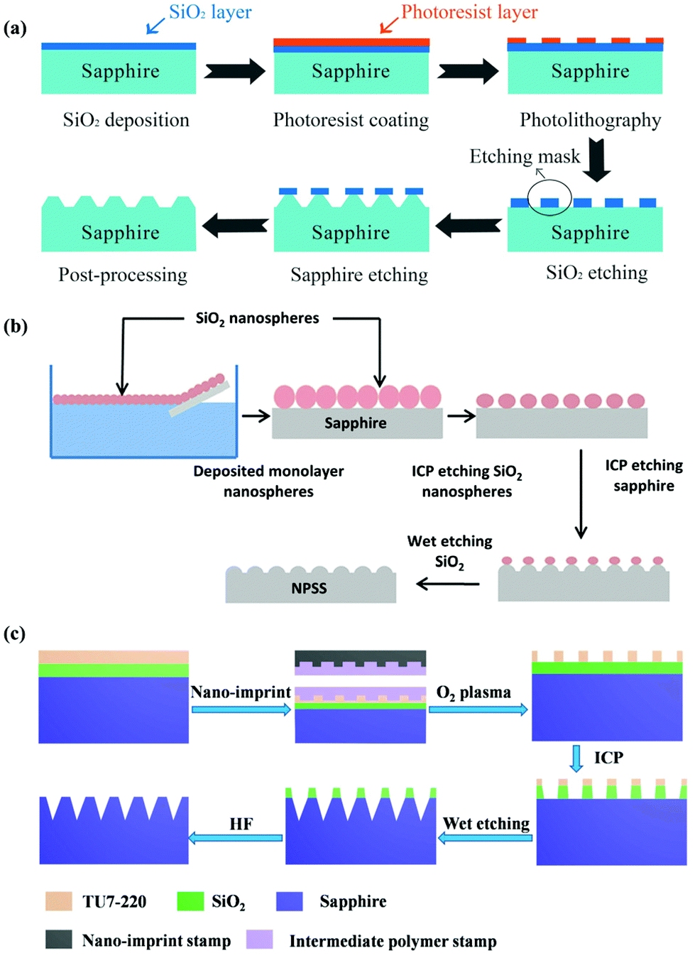 | ||
| Fig. 2 (a) The fabrication process flow for PSS. (b) The fabrication process flow for NPSS by self-assembled SiO2 nanosphere monolayer template. Reproduced with permission.44 Copyright 2014, American Institute of Physics Publishing. (c) The fabrication process flow for NPSS by nanoimprint lithography. Reproduced with permission.45 Copyright 2016, Springer Nature Publishing Group. | ||
Hsu et al.46 deposited a 500 nm-thick Ni layer on the c-plane of the sapphire substrate, and then the stripe-shaped Ni patterns were defined along the [1−100] direction by standard lithography. By selecting the flow rate ratio BCl3/(Cl2 + BCl3) properly, the 3 μm-width and 100 nm-depth stripe patterns were prepared, and the corresponding spacing between two stripes was 3 μm. At 20 mA, 35% enhancement in light output power (LOP) of LED grown on the PSS was achieved compared with that of LED grown on FSS, which may be ascribed to the reduced TDD and the improved LEE.53
Chang et al. fabricated LED on hemisphere-shaped PSS by combining photolithography, ICP and RIE. Firstly, the patterned polymethyl methacrylate (PMMA) was obtained by photolithography.47 By using the thermal reflow technique, the spacing between PMMA patterns was reduced to form the hemisphere-shaped PMMA. The PMMA patterns were subsequently transferred to the SiNx film by RIE, and the sapphire substrate was then etched by BCl3 plasma using ICP. Finally, the hemisphere-shaped PSS with 4.3 μm-diameter and 0.5 μm-spacing was produced. What's more, by adjusting the thickness ratio between SiNx and PMMA, researchers also fabricated the LED on stripe-shaped PSS. They found that the GaN grown on hemisphere-shaped and stripe-shaped PSS demonstrated similar TDDs, but the LOP of LED grown on hemisphere-shaped PSS was 13% higher than that of LED grown on stripe-shaped PSS. The improved LEE is owing to the inclined facets of hemisphere-shaped PSS. Wang et al. used standard lithography technology combined with the dry etching process to fabricate a periodic hole pattern array on c-plane sapphire.48 The diameter of the hole was 3 μm and the corresponding spacing between two patterns was also 3 μm. The LED grown on the proposed PSS with an optimum pattern depth (1.5 μm) demonstrated ∼21% enhancement in LOP at 20 mA compared with that grown on FSS.
We has combined BCl3/Ar plasma chemistry and SiO2 mask to fabricate patterns with several micrometres period on sapphire substrate.54 It is noted that the increase of BCl3 gas flow in pure BCl3 gas chemistry rapidly increased sapphire etch rates, which reached the maximum value when gas flow was 50 sccm. Then, the further increased BCl3 gas flow slowly decreased the etch rate. Moreover, the etch rate increased as the operating pressure decreased. Additionally, we have investigated the effect of input process parameters such as the ICP power/RF power, operating pressure, and Cl2/BCl3 gas mixing ratio on the etch characteristics of GaN films.55 The optimum ICP etching conditions (300 W ICP power/100 W RF power, 70 sccm of total flow rates, 90% Cl2/10% BCl3) for defining the mesa during the LED device fabrication were presented, which was also feasible for patterning of the sapphire substrate using the same plasma chemistry. Based on these findings, we applied thermally reflowed photoresist technique and BCl3-based ICP etching process to fabricate cone-shaped PSS for achieving highly efficient and reliable high power LEDs.56
Li et al.61 prepared LED on pyramid-shaped PSS fabricated by wet etching. The sapphire substrate with patterned SiO2 mask was immersed into H2SO4 solution and the constant etching temperature was 250 °C. Three types of PSS with average sizes of 4.8, 4.0 and 2.2 μm were prepared. They found that the dihedral angle between c-plane sapphire and side-plane of the pyramid increased with the decreasing size of the pyramid. The highest LOP was obtained in the LED with the smallest size of PSS.
Wang et al. investigated the effect of V-shaped PSS produced by the wet etching process on the LED performances.62 Firstly, a SiO2 layer with a thickness of 300 nm was prepared on the sapphire surface, and then the SiO2 layer was etched by standard lithography. By controlling the etching time, the sapphire substrate was then etched at 400 °C with stripe SiO2 as mask and H2SO4 as the etching solution. The residual SiO2 layer was removed by HF solution. The ridge width and period of PSS were 3.5 and 6.5 μm, respectively. They found that the V-shaped PSS effectively reduced the contact area between the GaN layer and substrate during the epitaxial growth, leading to reduced TDDs and enhanced crystalline quality of epilayers. Furthermore, Wu et al.63 found that the crystalline quality of GaN became better with the decreasing pattern spacing of V-shaped PSS because most of the growth of GaN was initiated from c-plane. However, it was difficult for GaN to grow on the sapphire when the pattern spacing was less than 0.41 μm, resulting in the degradation of crystalline quality of GaN.
In general, dry etching technique is capable of producing an anisotropic profile more efficiently compared with wet etching.64 However, dry etching suffers from the inherently strong physical component so that it has a low etch-selectivity between sapphire and the etching mask. In addition, ion bombardment may lead to contamination and damage to the surface of the sapphire substrate, which is detrimental to the quality of epitaxial layers.65 By contrast, wet etching possesses relatively high etch-selectivity and reduces the cost of fabricating PSS as compared to dry etching.
2.2 Nanometre-sized patterns transfer techniques
Zhang et al. proposed a self-assembly technology where a layer of SiO2 nanospheres with a diameter of 600 nm was coated on the sapphire substrate.44 Then the SiO2 nanospheres serving as the dry-etching mask were shrunk by the ICP etching process with CF4 (Fig. 2b). SiO2 nanospheres with different intervals (0, 50, and 120 nm) were obtained by controlling different etching time (0, 90, and 180 s). Chen et al. fabricated NPSS by nanosphere lithography.73 The polystyrene spheres were spun uniformly onto the surface of sapphire substrate, then the sapphire substrate was etched by using a mixture of Cl2 and BCl3 gases. The diameter, depth, and spacing of the proposed PSS were 450, 150 and 50 nm, respectively. Results of high-resolution X-ray diffraction and etch-pit density measurement inferred the improved crystalline quality of GaN epilayers. In addition, the LOP was increased by 30% and 11% for the LED on NPSS compared with the ones on PSS and on MPSS, respectively.
3. Effects of PSS on LEDs
It is well-known that EQE is a key performance parameter for III-nitride LEDs, which can be calculated by:| EQE = IQE × LEE | (1) |
3.1 Dislocation density reduction by PSS
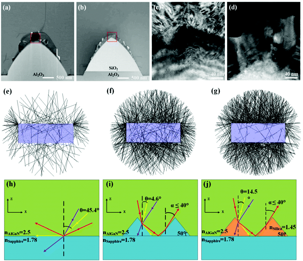
Heteroepitaxial growth of III-nitrides on sapphire substrate gives rise to strained films consisting of a high density of defects due to the large mismatch in the lattice and thermal expansion coefficients between the c-plane sapphire substrate and epilayers. Several types of defects have been reported, including threading dislocation,86 stacking fault,87 point defect,88 V-pit,89,90 trench defects91 and misfit dislocations.92 In particular, dislocations and point defects serve as nonradiative recombination centres that introduce the defect levels into the bandgap of III-nitrides and reduce the possibility of radiative recombination by capturing carriers, finally degrading the IQE of LEDs.93–96 Moreover, fundamental bottlenecks including efficiency droop97 and green gap98 encountered by III-nitride LEDs are found to be closely related with dislocation density, which adversely affects IQE and thus degrades optoelectronic properties of LED devices.To reduce the TDD in epilayers, a number of growth techniques have been investigated, consisting of epitaxial lateral overgrowth (ELO) technology and its derivatives, pendeo-epitaxy (PE) and facet-controlled epitaxial lateral overgrowth (FACELO).100–102 Generally, in the conventional ELO, GaN layer with thickness of several micrometres is first grown on substrate and then SiNx or SiO2 patterned masks are used to realize subsequent selective growth process.103 This technology, however, requires a growth interruption, which is time-consuming and easily introduces contaminations.104 In contrast, PSS technology that could be prepared before the epitaxial growth leads to single continuous growth process without contamination induced by mask. Employment of PSS enables significant reduction of TDDs at the interface between epilayers and substrate as well as LEE enhancement of LEDs.
Using low-temperature-(LT)-depostied GaN or AlN as buffer layer is an important method to diminish the lattice mismatch in the early development of LEDs.1,3 Through transmission electron microscopy (TEM) observation in Fig. 3a–f, we found that density of both screw dislocation and edge dislocation in GaN epilayer grown on PSS was much less than that in GaN epilayer grown on FSS.56 Compared to LED grown on FSS, LED grown on PSS showed higher sub-threshold forward-bias voltage and lower reverse leakage current, resulting in an enhancement in device reliability. Moreover, by adopting stripe-shaped SiO2 distributed current blocking layer, LOP of LED grown on PSS was further increased by 13%, which was attributed to the uniform current spreading.
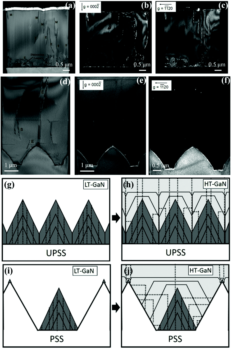 | ||
| Fig. 3 TEM images of GaN epitaxial layer grown on (a–c) FSS and (d–f) PSS. Reproduced with permission.56 Copyright 2015, Elsevier. Formation and propagation mechanism of dislocation with (g–h) FSS and (i–j) PSS. Reproduced with permission.99 Copyright 2018, Elsevier. | ||
Nie et al. explained mechanisms of dislocation formation and propagation in LED structures grown on FSS and PSS.99 For the case of FSS (Fig. 3g and h), dislocations originate from the internal pyramids and pyramid boundaries, while dislocations generated from the boundary coalescence could not be annihilated with the subsequent high temperature growth mode. In contrast, for the case of PSS (Fig. 3i and j), more spacings are provided for epitaxially lateral overgrowth (ELOG), and the number of initial islands is reduced, resulting in dislocation bending and minimization of island coalescence. V-defects associated with dislocations could be well minimized by adopting PSS. Moreover, the thickness of LT-GaN is found to affect the subsequent growth of GaN films due to the different nucleation sites during three-dimensional (3D) growth on PSS.
Another choice to improve the crystalline quality is to take the advantages of ex situ sputtered AlN nucleation layer (NL) over LT-GaN/AlN from the aspect of a lower TDD in epilayers and one-step growth. Chang et al. compared the GaN growth on high aspect ratio PSS with in situ LT-AlN NL and ex situ sputtered AlN NL.105 With in situ LT-AlN NL, the GaN growth occurs on the c-plane and pattern region, and the laterally overgrown GaN from both regions subsequently coalesces, causing the creation of irregular voids. However, with the sputtered AlN NL, a different growth behaviour is observed that the sputtered AlN NL not only increases vertical growth from c-plane region, but also suppresses lateral growth from the cone region, leading to high-quality GaN epilayers without void formation and enhancement in LOP by 47.7%. Moreover, by adjusting growth modes, different GaN growth behaviours occurred on the PSS with sputtered AlN NL.106 Under “tsunami” growth mode, GaN grows into truncated pyramid shape, which facilitates the dislocation bending from flat area toward inclined planes, and especially the dislocation propagation in grains on the conical surface is inhibited. However, under “rising tide” growth mode, dislocations on the conical surface have the possibility to extend upward. Accordingly, the GaN layer grown under “tsunami” growth mode has a lower TDD than that grown under “rising tide” growth mode.
We reported and compared UV LEDs grown on ex situ sputtered AlN NL/PSS, in situ LT-GaN NL/PSS and LT-AlGaN NL/PSS.107 It was found that the UV LED on ex situ sputtered AlN NL/PSS exhibited the lowest TDD among three types of UV LEDs (Fig. 4a–i). The LOP of the UV LED on ex situ sputtered AlN NL/PSS was 11.2% higher than that of the UV LEDs on in situ LT-AlGaN NL/PSS, which could be attributed to the reduced TDD in the active region grown on ex situ sputtered AlN NL/PSS. The results indicated that the introduction of ex situ sputtered AlN NL/PSS was an effective method to enhance the performance of UV LED.
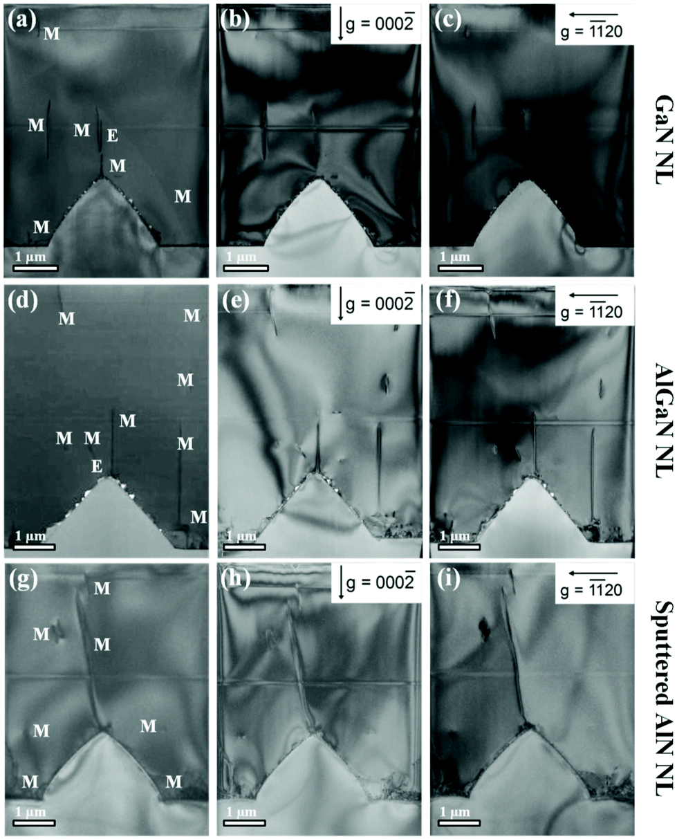 | ||
| Fig. 4 Cross-sectional TEM images of UV LEDs grown on (a–c) LT-GaN NL/PSS, (d–f) LT-AlGaN NL/PSS and (g–f) sputtered AlN NL/PSS. The edge (E) and mixed (M) type dislocations are marked. Reproduced with permission.107 Copyright 2017, Springer Nature Publishing Group. | ||
By using ex situ sputtered AlN NL/PSS, we further investigated the effect of PSS size on the GaN-based UV LED performance.108 The bottom diameter/height/spacing values of cone-shaped PSS were 0.73 μm/0.46 μm/0.27 μm, 1.8 μm/1.1 μm/0.2 μm, and 2.7 μm/1.7 μm/0.3 μm for PSS-I, PSS-II, and PSS-III, respectively. The fill factor was defined as the ratio of the pattern area to the total area. The calculated fill factors for PSS-I, PSS-II, and PSS-III were 0.4, 0.65 and 0.71, respectively. It was found that the increasing pattern size of PSS could lead to the reduced TDD (Fig. 5a–i). That was because the flat c-plane area of the bottom of PSS decreased when the size of PSS increased, thereby resulting in the decrease in the initial density of GaN islands and the longer lateral growth time of GaN epilayers. As a result, the LOP of UV LED grown on PSS with fill factor of 0.71 was 131.8% higher than that of the UV LED grown on PSS with a fill factor of 0.4.
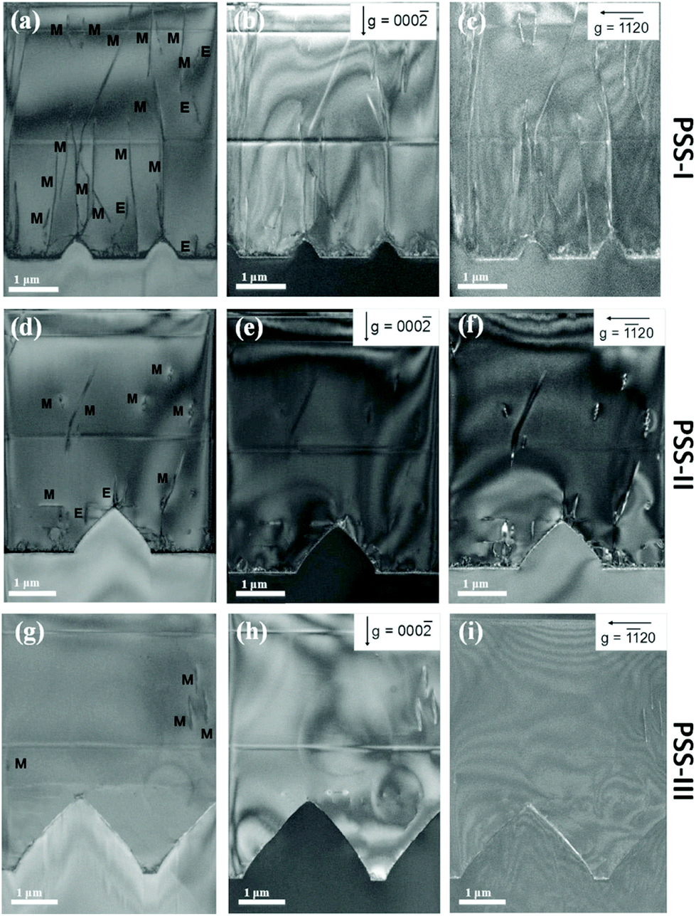 | ||
| Fig. 5 Cross-sectional TEM images of UV LEDs grown on (a–c) PSS I, (d–f) PSS II and (g–i) PSS III. The screw (S), edge (E), and mixed (M) type dislocations are marked. Reproduced with permission.108 Copyright 2017, Institute of Physics. | ||
The effect of isoelectronic Al doping in GaN buffer layer on UV LED crystalline quality and optoelectronic properties was also investigated.109 It was found that the overall TDD and the background carrier concentration could be reduced in the isoelectronically Al-doped GaN buffer layer as compared to undoped GaN buffer layer. Especially, the screw-type dislocation density was effectively reduced by isoelectronic Al doping. With optimum isoelectronic Al doping concentration of 0.18% in GaN buffer layer, UV LED exhibited 7.6% increase in LOP due to the improved crystalline quality.
To straightforward understand the dislocation annihilation mechanism, schematic illustrations of growth evolution for ELOG of AlN epilayers on NPSS are exhibited in Fig. 6.110 The dislocations are marked as blue colour. The V/III ratio strongly affects the surface mobility of Al adatoms that usually accompanies the transition of the growth mode between 3D and 2D mode.111 At initial growth stage in Fig. 6a, AlN with high V/III ratio (H-V/III AlN) is grown on NPSS dominated by 3D growth mode. The high V/III ratio facilitates the formation of island crystals with abundant crystal boundaries to suppress the elongation of dislocations.112 However, there are still a number of dislocations existing in H-V/III AlN layer. Therefore, AlN layer with low V/III ratio (L-V/III AlN) is deposited on the H-V/III AlN because the low V/III ratio facilitates the 2D growth of AlN epilayer by smoothening the surface. Owing to the transition of growth mode from 3D to 2D, some dislocations are terminated by merging with each other in Fig. 6b. After that, a 3-period AlN superlattices with alternating high and low V/III ratios (LH-V/III AlN SL) structure is deposited on the L-V/III AlN. Because SL layers can bend dislocations,113 most dislocations are eliminated in the 3-period LH-V/III AlN SL structure in Fig. 6c. In addition, some dislocations could also be terminated on the internal surface of arrow-shaped ELOG voids in Fig. 6c and d. Ultimately, the thick L-V/III AlN is deposited on AlN SLs to flatten the AlN epilayer surface. It is noted that few dislocations eventually propagate through the thick L-V/III AlN in Fig. 6d.
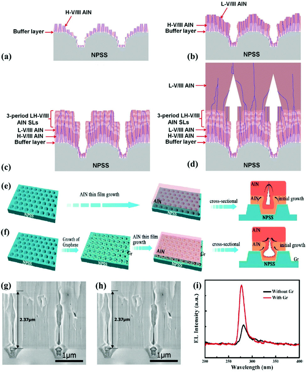 | ||
| Fig. 6 (a–d) Schematic illustrations of growth evolution for AlN epilayers on NPSS. Reproduced with permission.110 Copyright 2018, Elsevier. Schematic diagrams of AlN growth on (e) bare NPSS and (f) Gr/NPSS. Cross-sectional schematic diagrams of AlN films grown on (g) bare NPSS and (h) Gr/NPSS. (i) EL spectra of the DUV-LEDs with and without the graphene interlayer. Reproduced with permission.116 Copyright 2019, American Institute of Physics Publishing. | ||
Newly emerging quasi-van der Waals epitaxial (QvdWE), which opens the door to growing high-quality III-nitride materials on hybrid substrates made of 2D materials and sapphire, has been adopted to overcome lattice mismatch limitation and achieve flexible devices.114,115 Chang et al. reported the growth of high-quality AlN films on NPSS by graphene (Gr)-assisted QvdWE.116 It is found that AlN exhibits the 3D longitudinal island growth mode and the lateral coalescence of the AlN nucleation islands is relatively slow, hard to cover the NPSS at a thin growth thickness (Fig. 6e and g). In contrast, because Al adatoms diffuse easily on the surface of Gr/NPSS, AlN prefers the lateral 2D growth mode, leading to rapid and lateral coalescence with a thin and flat AlN film (Fig. 6f and h). Benefiting from the Gr interlayer, a reduction of TDD and 2.6 times enhancement in EL intensity have been achieved in DUV-LEDs grown on Gr/NPSS (Fig. 6i).
3.2 LEE enhancement by PSS
nGaN![[thin space (1/6-em)]](https://www.rsc.org/images/entities/char_2009.gif) sinϕ = nairsinΦ sinϕ = nairsinΦ | (2) |
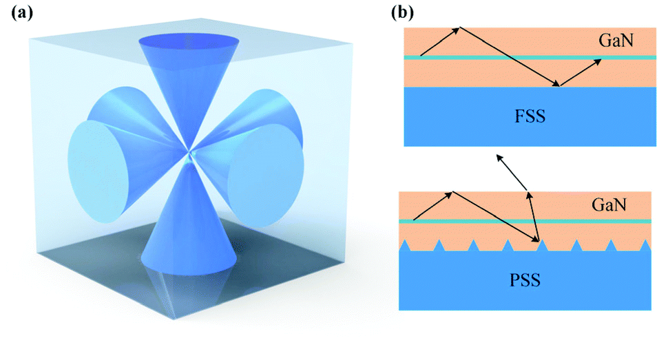
For LEDs, critical angle (ϕc) of TIR is calculated to be 23.6° when the Φ is 90°. In other words, light with an incident angle less than 23.6° can escape from GaN into air, whereas light with an incident angle exceeding 23.6° will be reflected back. Similarly, the ϕc of TIR at GaN (n = 2.5)/sapphire (n = 1.7) interface can be estimated to be 42.8°, indicating that light will also be reflected back at GaN/FSS interface. The light escape cone is defined by the ϕc of TIR, which takes the luminous point as the vertex and 2ϕc as the apex angle, as is shown in Fig. 7a. Only lights emitted inside the light escape cone can escape from semiconductor chip into air.
 | ||
| Fig. 7 Schematic of (a) light escape cone for LED and (b) light trajectories in LEDs with FSS and PSS. | ||
For LEDs grown on sapphire substrate, the polarization modes of light can be characterized as transverse-electric (TE) polarized mode and transverse-magnetic (TM) polarized mode by the direction of electric field relative to the c-axis. The visible and near-infrared lights are mainly TE polarized, where the electric field vector is perpendicular to c-axis.117 However, for UV lights and particularly for deep UV lights, TM-polarized lights increase with the increment of Al composition in AlGaN QWs or decrement of emission wavelength, where the electric field vector is parallel to c-axis. Compared with TE-polarized lights, TM-polarized lights are affected by TIR more greatly, due to large incident angle caused by lateral propagation mode.118 In addition, the p-GaN layer used for ohmic contact exhibits a strong absorption of UV lights.119,120 These detrimental factors cause the light to be trapped in semiconductor chip and finally reabsorbed by epilayers or electrodes, thereby deteriorating the light extraction of LEDs. However, the light scattering effect of PSS can modify the light path, which will raise the probability of light entering into the escape cone, as shown in Fig. 7b. As a result, more lights can propagate into air and thus improve the LEE of LEDs.29,40
 | (3) |
4. Influence of structural parameters of PSS on LED properties
As mentioned above, patterns on PSS could be fabricated with different sizes (from microscale to nanoscale), different shapes (cone, hemisphere, stripe, volcano, etc.) and other related structural parameters (diameter, height, spacing, slanted angle, etc.). Herein, we will described representative examples, comparing and illustrating the influence of PSS structural parameters on the LED performances based on experimental and simulation results, which are summarized in Table 1.| Shape | Pattern size (μm) | Properties | Ref. |
|---|---|---|---|
| The “TDD reduction”, “EQE enhancement”, “enhanced crystalline quality”, “reduced TDD” and “LEE enhancement” statements in column “properties” refer to the III-nitride films or LEDs grown on PSS compared with those grown on FSS if no special instructions. | |||
| Cylindrical hole | Diameter/period: 0.25/0.45 | TDD reduction: 44% | 127 |
| EQE enhancement: 260% (20 mA) | |||
| Cone | Height/bottom diameter/interval: 0.5/0.7/0.3 | LEE enhancement: 78% | 132 |
| Cone | Height/bottom diameter/interval: 1.5/2.5/0.5 | Reduced TDD | 56 |
| Cone | Height/bottom diameter/interval: 0.15/0.45/0.05 | Enhanced crystalline quality | 134 |
| EQE Enhancement: 30% (20 mA) | |||
| Cone | Height/bottom diameter/interval: 1.5/2.7/0.2 | TDD reduction: 76% | 135 |
| Cone | Height/bottom diameter/interval: 1.7/2.7/0.3 | Reduced TDD | 108 |
| EQE enhancement: 130% (20 mA) (compared with smaller-sized PSS) | |||
| Cone | Height/bottom diameter/interval: 1.2/3.0/6.0 | Reduced TDD | 49 |
| Cone | Height/bottom diameter/interval: 1.5/3.0/1.0 | LOP enhancement: 34% (20 mA) | 161 |
| Cone | Height/bottom diameter/interval: 1.6/2.65/3.0 | LEE enhancement: 60% | 150 |
| LOP enhancement: 82% (20 mA) | |||
| Stripe | Groove width/spacing/depth: 3.0/5.0/0.9 | Reduced TDD (compared with smaller-depth PSS) | 137 |
| Stripe | Groove width/ridge width/depth: 3.0/3.0/1.5 | LOP enhancement: 20% (20 mA) | 138 |
| Pillar | Height/diameter/period: 0.1/0.11/0.25 | EQE enhancement: 30% (100 mA) | 146 |
| Volcano | Diameter/spacing/depth: 2/1.0/1.5 | LEE enhancement: 62% | 139 |
| Volcano | Diameter/spacing/depth: 0.4/1.0/0.5 | TDD reduction: 30% | 141 |
| LEE enhancement: 21% (compared with cone-shaped NPSS) | |||
| Volcano | Diameter/spacing/depth: 5.0/9.0/0.4 | LEE enhancement: 103% | 142 |
| LOP enhancement: 40% (350 mA) | |||
| Volcano | Diameter/spacing/depth: 2.2/3.0/0.6 | LEE enhancement: 21% | 79 |
| Hemisphere | Diameter/spacing/height: 0.5/0.2/0.2 | EQE enhancement: 27% (20 mA) | 148 |
| Hemisphere | Diameter/spacing/height: 3.5/0.8/1.2 | LOP enhancement: 14% (350 mA) | 162 |
| Spherical cap | Radius/height/edge spacing: 3.4/2.78/1.7 | EL intensity enhancement: 15% (compared with cone-shaped PSS) | 154 |
| Concave hole | Average diameter/depth: 0.2/0.1 | LEE enhancement: 60% | 74 |
| Concave hole | Diameter/depth/spacing: 3.0/1.5/3.0 | EQE enhancement: 20% (20 mA) | 147 |
| Hexagonal hole | Diameter/period: 0.65/1.0 | Reduced TDD | 45 |
| Hexagonal hole | Depth/period: 0.2/1.0 | TDD reduction: 92.65% (compared with pillar-shaped NPSS) | 144 |
| Double-side hole | Diameter/depth/spacing: 3.0/1.0/3.0 | LOP enhancement: 53% (350 mA) | 158 |
| Truncated pyramid | Height/bottom diameter/interval: 0.4/0.4/0.4 | EQE enhancement: >50% (20 mA) | 41 |
| Double-side hemisphere | Diameter/height/spacing: 0.16/0.05/0.1 | TM-polarized LEE enhancement: 11.2 times | 159 |
| Moth-eye microstructure | Height/bottom diameter/interval: 1.75/2.5/3.0 | LEE enhancement: 200% | 160 |
4.1 LEDs on PSS with micrometre-scale and nanometre-scales patterns
NIL was used to fabricate NPSS with hexagonal array of cylindrical holes, whose diameter was 250 nm and period was 450 nm.127 From the TEM analysis (Fig. 8a and b), a lower TDD of 3.6 × 108 cm−2 was found at NPSS/GaN interface and the existence of void indicated the overgrowth in lateral direction. The mechanism of TD formation is illustrated as follows (Fig. 8c and d). TDs generated from the bottom of the etched sapphire (T3) are mostly interrupted by voids, and TDs generated from the inclined plane change direction to propagate within the growth plane (T2). Only TD generated from the unetched region of NPSS (T1) will propagate to the active region. Benefiting from the decreased TDD, both IQE and EQE of NPSS LED were increased as compared to FSS LED (Fig. 8e and f). Furthermore, photonic crystal effect is possibly induced at GaN/PSS interface. The photonic crystal is an ordered, periodic structure made up of materials with alternating refractive indices, in which light propagation could be effectively controlled.128,129 In this NPSS strategy, the LEE enhancement is not only related to the light scattering, but also to the constructive interference of scattered light, which contributes to better LED performance compared to MPSS and FSS.130,131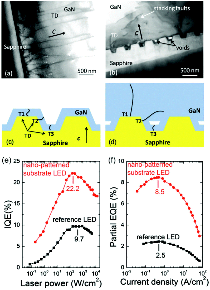 | ||
| Fig. 8 Cross-sectional TEM of the epitaxial GaN/sapphire interface on (a) FSS and (b) NPSS. Schematics show (c) early and (d) late phases of the TD (T1, T2, T3) formation on NPSS. (e) IQE as a function of excitation power density. (f) EQE as a function of current density for NPSS LED. Reproduced with permission.127 Copyright 2011, American Institute of Physics Publishing. | ||
Except for visible LEDs, NPSS also enhances LEE of DUV LEDs, due to the increment of extraction for TM-polarized lights. In our previous study, we have investigated the LEE of DUV LEDs using FDTD method.132 The results showed that NPSS could enhance the LEE of TM-polarized lights significantly, as compared to FSS. Furthermore, the LEE of flip-chip LED on NPSS was estimated to be about 15%, which was ∼50% higher than that of flip-chip DUV LED with rough n-AlGaN surface (Fig. 9). Recently, it is reported that the combination of NPSS and meshed p-GaN can remarkably increase the LEE for both the TE-polarized and the TM-polarized light.133
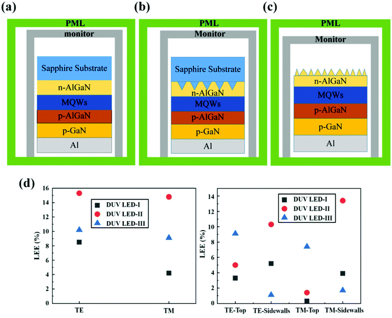 | ||
| Fig. 9 Simulation model of (a) flip-chip DUV LED on FSS (DUV LED-I), (b) flip-chip DUV LED on NPSS (DUV LED-II), and (c) flip-chip DUV LED with roughed n-AlGaN surface (DUV LED-III). (d) Simulated LEE of DUV LED-I, DUV LED-II, and DUV LED-III. Reproduced with permission.132 Copyright 2020, Institute of Physics. | ||
NPSS shows better LEE due to the increased number of patterns that increase the probability of light scattering. However, smaller pattern size of PSS not always leads to better LED performance. In the situation of GaN grown on PSS-2 μm (diameter/spacing/depth: 2 μm/2 μm/1.5 μm), PSS-3 μm (diameter/spacing/depth: 3 μm/3 μm/1.5 μm), NPSS (diameter/spacing/depth: 450 nm/50 nm/150 nm) and FSS corresponding to Fig. 8a–d, GaN film on NPSS shows a higher etch-pit density and broader full-width at half-maximums (FWHMs) of the ω scan rocking curve for both (002) and (102) planes.134 It indicates that the crystalline quality does not show an absolute dependence on the pattern size, and epilayers grown on MPSS show better crystal quality than NPSS in some cases.135
As the parameters of patterns for sapphire substrate will remarkably influence LEE, the LEE of LEDs on PSS is expected to be further improved when the pattern size varies from the micrometre to nanometre. However, it is noted that the strong diffraction induced by near-wavelength-scale patterns will not enhance the LEE of LEDs effectively.136 On the contrary, micro-scale patterns at a specific aspect ratio (defined as the ratio of the structure height to the structure width) and subwavelength-scale patterns will contribute to marked enhancement of LEE.
4.2 LEDs on PSS with various shapes
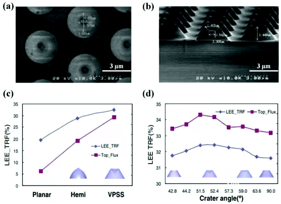 | ||
| Fig. 10 (a–b) SEM images of volcano-shaped PSS. (c–d) Simulated LEE as a function of crater angle and the LEE of FSS, hemispherical and volcano-shaped PSS. Reproduced with permission.139 Copyright 2010, Institute of Physics. | ||
After that, simplified fabrication methods of volcano-PSS, such as colloidal monolayer templating and NIL were employed.79,140,141 Embedding SiO2 layer in volcano-shaped PSS, which suppressed the GaN growth, could result in fewer threading dislocations in GaN epilayer.142 Conical air voids were formed in the crater, which decreased the residual compressive strain and improved LEE. The simulation results based on FDTD method showed that the conical air voids could turn the light path towards the top surface, due to the large difference in refractive index at the air/GaN interface. Meanwhile, the silica layer can mitigate the refractive index mismatch between the GaN and air, thereby improving LEE of light trapped in the conical air voids (Fig. 11).
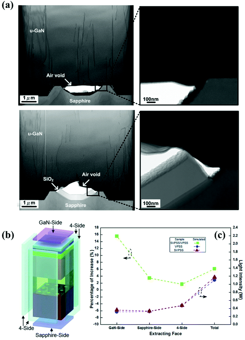 | ||
| Fig. 11 (a) TEM images of LEDs grown on volcano-shaped PSS (VPSS) and volcano-shaped PSS with embedded SiO2 (SVPSS). (b) Schematic of different receiver positions in the simulation. (c) Light intensity and percentage increase in light intensity of LEDs grown on the VPSS and SVPSS. Reproduced with permission.142 Copyright 2015, Royal Society of Chemistry. | ||
4.3 LEDs on PSS with various structural parameters
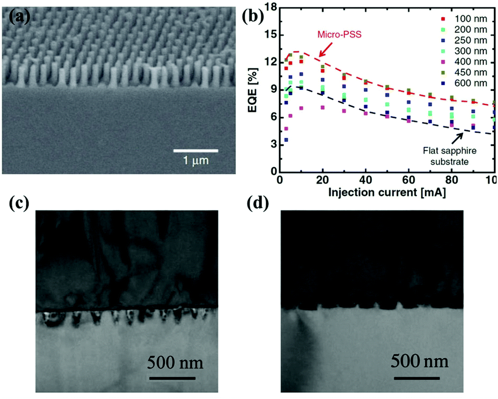 | ||
| Fig. 12 (a) SEM image of NPSS with pillar height of 600 nm. (b) EQEs of LED chips on nano-PSSs as a function of injection current. Reproduced with permission.146 Copyright 2013, Institute of Physics Publishing. TEM images of the GaN thin films grown on (c) high aspect ratio and (d) low aspect ratio NPSS. Reproduced with permission.149 Copyright 2016, Elsevier. | ||
Aspect ratio of NPSS was demonstrated to induce different growth behaviours and improve the crystal quality.149 For NPSS with high aspect ratios (height/diameter: 2) shown in Fig. 12c, GaN growth started from both the flat-top and bottom of patterns. Nevertheless, the quick-merging GaN obstructed the continuous GaN growth on the bottom of patterns, leading to the void formation. Consequently, TDs generated from the bottom of patterns were prevented. As for the NPSS with low aspect ratio (height/diameter: 0.7) in Fig. 12d, the growth on the bottom and top of the patterns took place simultaneously until the GaN film filled the whole patterns without voids. The competition of lateral growth and vertical growth increased edge-type TDD. Accordingly, high aspect ratio NPSS induced a higher proportion of lateral growth, thereby enabling the better crystal quality due to TD bending. Besides, high aspect ratio NPSS improved electrical properties including mobility and concentration in GaN films in comparison with low aspect ratio NPSS and bare sapphire.
LEEs of blue LEDs grown on truncated pyramidal shaped-NPSS with various spacing (200, 400, 600, and 800 nm) were in the range of 38% to 42%, which were higher than that of LEDs grown on FSS (∼29%).41 LED grown on the 200 nm-spacing NPSS presented the maximum EQE of 54% at 25 mA, while the maximum EQE of LED grown on FSS was 35% at 49 mA.
4.4 Comprehensive comparison of LEDs on PSS with different structural parameters
The improvement of LEE using PSS is attributed to light scattering effect, which will be influenced by the geometric parameters of patterns. Jang et al. theoretically investigated pattern shapes (cylindrical, conic, and hemispherical patterns) and sizes (height and diameter) of PSS based on the ray-tracing method, pointing out that the LED on hemispherical PSS (1.5 μm-height and 4.5 μm-diameter) showed the best light extraction efficiency.152 Another optimization of hemispherical PSS by combing ray-tracing and FDTD methods has implied that the optimal radius for the hemispherical patterns is around the emission wavelength of the devices.153 The hemispherical patterns can modulate the angles of reflection and transmission, which reduces incidence angles of light at GaN/air and sapphire/air interfaces and thereby improved the light extraction. Wang et al. proposed spherical cap-shaped PSS based on the hemispherical PSS.154 They confirmed that spherical cap-shaped PSS with specific intercepted ratio and edge spacing could improve the LEE of LED more effectively, as compared to hemispherical PSS (Fig. 13a–c).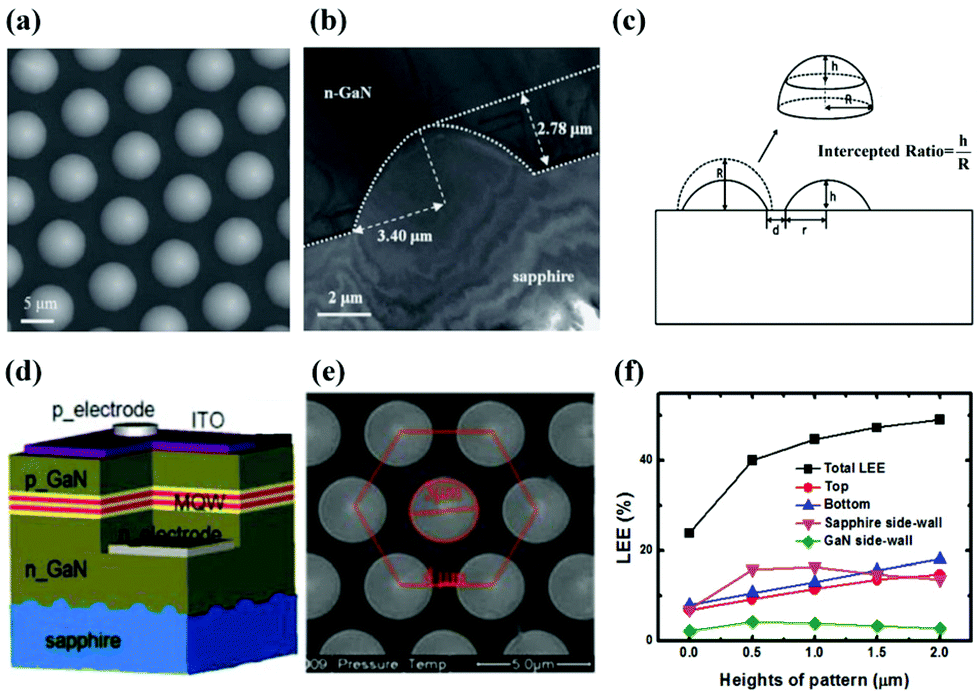 | ||
| Fig. 13 (a) SEM and (b) TEM images of spherical cap-shaped PSS and (c) schematic of spherical cap-shaped PSS with specific intercepted ratio (h/R) and edge spacing. Reproduced with permission.154 Copyright 2013, Institute of Physics. (d–e) Schematic of LED with cone-shaped PSS and simulated LEE as a function of pattern heights. Reproduced with permission.155 Copyright 2011, John Wiley and Sons. | ||
Moreover, the cone-shaped PSS is widely applied. It has been reported that the LEE of blue LEDs (∼455 nm) grown on cone-shaped PSS was increased with the pattern height, whereas the LEE tended to be saturated when height was over 1.5 μm due to the reduction of emission from the sidewall (Fig. 13d–f).155 Additionally, LEE of LEDs with cone-shaped PSS mainly hinged on the microstructure surface slope, which increased with increasing slope and reached a plateau when the slope exceeded 0.6.156
We have reported that microstructures (cone, truncated cone, hemisphere, and pyramid) on the top surface of sapphire substrate can enhance the LEE of flip-chip blue micro-LEDs via designing their shapes and heights.157 However, we also suggest that surface texture is less efficient than the PSS for increasing the LEE in an encapsulated LED. This is because the effect of surface texture is almost eliminated, due to the small refractive index difference between sapphire substrate and encapsulation. Furthermore, the double-side PSS was reported to enhance the LEE of LEDs.158 Notably, the double-side PSS with macrodome-shaped array were numerically analyzed using FDTD method, which can achieve ∼2.6 times and ∼11.2 times enhancement in LEE of TM-polarized lights for 230 and 280 nm DUV LEDs, respectively.159 What is more, the moth-eye microstructure on the backside of sapphire substrate can significantly weaken the TIR at the sapphire/air interface and enlarge the light extraction angle, which approximately doubled the LEE of DUV LEDs.160
4.5 Semipolar III-nitride LED on PSS
III-nitride LEDs grown on c-plane sapphire suffer from QCSE owing to the strong built-in polarization field, which reduces the electron–hole wavefunction overlap and the radiative recombination rate, thereby severely decreasing the IQE.163 To overcome this problem, bulk GaN substrate has been confirmed to be successful for the growth of efficient semipolar LED. The bulk GaN is typically prepared by HVPE or ammonothermal growth and subsequently sliced to desired orientation as free-standing GaN substrate. Considering the high fabrication cost and limited size available, it is not practical for mass production to satisfy commercial application demand. Therefore, pursuing appropriate foreign substrates for epitaxial growth is highly desirable. Semipolar GaN could be selectively grown on the sidewalls of stripe-shaped PSS,164,165 similar as GaN grown on the inclined sidewalls of stripe-patterned silicon.166Song et al. achieved purely nitrogen polar semipolar (20−21) GaN epilayers on the inclined c-plane sidewalls of patterned (22−43) sapphire substrates.167 A 490 nm LED fabricated on (20−21) GaN showed a reduced blueshift compared to LED grown on c-plane GaN. To grow high-quality semipolar GaN, Ge doping was introduced during the growth.87 Ge doping was found to suppress the occurrence of N-polar GaN (000−1) facets, leading to the elimination of SFs generated in (000−1) facet. Blue LED grown on SF-free similar GaN exhibited a similar LOP as the LED on GaN bulk substrate. Currently, (20−21) blue LED on PSS was reported to exhibit IQE up to 52%.168 It is well known that high Indium content is required for LEDs with long-wavelength emission. Inevitably, indium clusters form in InGaN QWs because of the spinodal decomposition, which severely affects the uniformity of QWs. Previous work by Li et al. illustrated In-cluster-free (11−22) GaN by controlling the nucleation facet size to around 500 nm and optimizing three consecutive procedures to form air voids.169 A record BSF density of 70 cm−1 and TD density of 5 × 107 cm−2 were achieved.
Okada et al.170 evaluated the LEE of semipolar (11−22) green LED on r-plane (1−102) PSS by ray-tracing method (Fig. 14). The results showed that the air voids between the GaN and r-plane PSS acted as a light-scattering structure, which reflected larger number of rays towards the top surface. As a result, the LEE of LED on the r-plane PSS was 68.5%, which was higher than that of the LED (60.0%) on PSS without air voids. Later, efficient semipolar (11−22) green micro-LED was fabricated, which showed a smaller blueshift than c-plane LED and especially a size-independent EQE of 2%, paving a way for large-area display application.171
 | ||
| Fig. 14 (a) Cross-sectional SEM images of (11−22) GaN layer on r-plane PSS. (b) Ray tracing result of (11−22) LED structure on r-plane PSS with embedded air voids. Reproduced with permission.170 Copyright 2011, John Wiley and Sons. | ||
Polarized phosphor-free white semipolar LEDs on (20−21) GaN/patterned sapphire template has been presented, which showed a LOP of 3.9 mW at 100 mA and especially a high 3 dB modulation bandwidth of 660 MHz for visible light communication application.172 The light radiation distribution pattern of white LED could be defined by the pattern morphology of PSS, leading to better white-light package efficiency and uniform illumination.173,174 Besides, semipolar green micro-LED showed small blue-shift and size-independent peak EQE of 2%. An interesting strategy combining semipolar micro-LED with perovskite nanocrystals was proposed for both visible light communication and full-color display.175
4.6 PSS derivatives
 | ||
| Fig. 15 Cross-sectional STEM images of AlGaN grown (a) on PSS and (b) PSSA. (c) Enlarged STEM images of the marked areas in (a) and (d) that in (b). Cross-sectional ray-tracing images of top-emitting UV LEDs on (e) FSS, (f) PSS, and (g) PSSA. Schematic illustration of light trajectories in top-emitting UV LEDs on (h) FSS, (i) PSS, and (j) PSSA. Reproduced with permission.24 Copyright 2019, Elsevier. | ||
We have also proposed PSSA substrate to improve LEE of flip-chip blue LEDs.176 The light trajectories in flip-chip blue LEDs on FSS, PSS, and PSSA are shown in Fig. 16. Since the ϕc of TIR at sapphire/air interface is calculated to be 34°, lights propagated from GaN or silica into sapphire with an incident angle less than 34° can finally escape from sapphire into air. That is, the extraction angle of light for FSS, PSS and PSSA is (0°, 24°), (10°, 40°) and (20°, 48°), respectively. Consequently, PSSA will enhance the extraction probability of lights with incident angle larger than the ϕc of TIR at the GaN/sapphire interface (∼46°). Additionally, the refraction angle of lights at sapphire/GaN interface is between 0° and 34°, whereas that of lights at silica/GaN interface is between 0° and 24°. In other words, light emission of the flip-chip LED on PSSA is more collimated, as compared to the flip-chip LED on PSS.
 | ||
| Fig. 16 Cross-sectional ray-tracing images of flip-chip blue LEDs on (a) FSS, (b) PSS, and (c) PSSA. (d) Schematic illustration of light trajectories in flip-chip blue LEDs on FSS, PSS, and PSSA. Reproduced with permission.176 Copyright 2020, Optical Society of America. | ||
 | ||
| Fig. 17 (a) Top-view SEM images of MPSS and NMCPSS and cross-sectional FDTD simulation images of light intensity distribution of FSS, MPSS- and NMCPSS-based LEDs. Reproduced with permission.178 Copyright 2013, Institute of Physics. (b) Top-view SEM images and light tracing schematic diagrams of MPSS and NMCPSS. Reproduced with permission.179 Copyright 2016, American Chemical Society. | ||
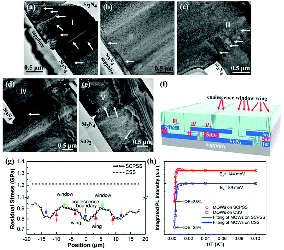 | ||
| Fig. 18 (a–e) Cross-sectional TEM bright field images with [01−10] zone axis of region I–V on SCPSS and (f) corresponding schematic diagram of dislocation evolution. (g) Stress distribution of MQW sample on SCPSS is compared with the MQW sample on conventional sapphire substrate (CSS). (h) Normalized integrated PL intensity of MQW emission as a function of temperature from 10 to 300 K for the MQW samples on SCPSS and CSS. Reproduced with permission.181 Copyright 2016, American Chemical Society. | ||
5. Summary and prospect
With the increasing demands for energy-saving and high-performance lighting sources, III-nitride LEDs are undoubtedly presumed to be the next-generation candidate with great potential. Development of heteroepitaxy technology provides a versatile route that III-nitride LEDs could be grown on low-cost foreign substrates. Particularly profiting from QvdWE,183 LED devices fabricated on the sapphire and glass have been successfully achieved in recent years.184,185 However, there are still bottlenecks lying ahead to achieve efficient III-nitride LEDs with regards to improving crystal quality and LEE. Currently, PSS technology acting as an effective method addresses the aforementioned issues simultaneously. Compared to FSS, the reduction of TDD by using PSS arises from the different growth behaviour. For epilayers grown on PSS, ELOG prevents a portion of TDs from propagating towards MQWs and leads to TDs bending, eventually decreasing the TDD. Notably, efforts devoted to optimizing growth techniques combined with PSS are indispensable for crystalline quality improvement. Furthermore, the mechanism of enhancing LEE by PSS is attributed to the increased chance of scattering light out of LED structure. The role of PSS closely associates with its structural parameters, such as pattern size, shape and aspect ratio, which have a considerable influence on the LED performance. Patterns with various structural parameters could be obtained by utilizing one certain or integrated method. Although PSS has shown remarkable significance for LEDs, there is still a long way to go for the further research. We believe that PSS technology applied in the LED filed may develop towards the following directions in the future.5.1 Integrated fabrication method for large-scale and uniform PSS with complicated patterns
Inspired by volcano-shaped PSS, we find the necessity of combining conventional etching methods with nanoimprint or nanosphere technique to explore the potential value of PSS. On the one hand, the crystal quality is expected to be improved for epilayers grown on PSS featuring complicated patterns. This is because the increased facets provide more nucleation sites for the subsequent ELOG. On the other hand, benefiting from the increased facets, more light will be scattered out of the LED structure, thus leading to higher LEE. Undoubtedly, integrated method is needed in the manufacture of complicated patterns on PSS. It should be mentioned that the pattern uniformity undergoes serious degradation through multiple processing steps, therefore it is hard to achieve large-scale PSS to meet the demands in practical applications. The research will center around how to make use of the advantages of various fabrication methods and at the same time introduce as little damage or contamination as possible. In order to achieve this goal, more in-depth investigation of PSS process condition is required.5.2 Optimizing the structural parameters of PSS for specific LED application
In spite of vigorous efforts for presenting the superiority of PSS than FSS, comparison of different PSS types for LEDs is insufficient. Besides, same PSS type with changing structural parameter is yet to be investigated for LEDs. The practical significance of this project is that an appropriately designed PSS contributes to maximize the LED efficiency and we need to take the LED structure, growth mode, growth conditions, and other factors into consideration. It is hard to draw any firm conclusion about which type or structural parameter of PSS is the best for LED applications. Furthermore, reasonable optimization based on experiments together with the numerical simulation will provide reliable evidence and encourage the development of high-efficiency LED grown on PSS.5.3 PSS derivatives and emerging technique with QvdWE
PSS derivatives show the feasibility of using other materials (e.g. SiO2, SiNx, and metal film) as patterns on the sapphire substrate to further improve LED performances. While PSS enables the decrease in TDs to some extent, the formation of TD arising from the lattice mismatch could not be avoided. Emerging QvdWE offers a robust solution to solve this problem. Prior to the epitaxial growth of III-nitrides, high-quality epilayers could be obtained by introducing graphene as buffer layer. To date, research on this technique combined with PSS is still in its infancy, which needs further improvement and exploration for highly efficient III-nitride LEDs.Author contributions
S. Z., X. Z., P. D., Z. Z and X. L. wrote the paper. L. G., S. L. and S. Z. revised the paper. All authors discussed the results and assisted during manuscript preparation.Conflicts of interest
There are no conflicts to declare.Acknowledgements
This research was funded by the National Natural Science Foundation of China (Grant Nos 51775387, 52075394 and 51675386), the National Key Research and Development Program of China (No. 2021YFB3600200) and the National Youth Talent Support Program. L. G. acknowledges support from the University of Michigan during his sabbatical leave when the manuscript was prepared.References
- H. Amano, N. Sawaki, I. Akasaki and Y. Toyoda, Appl. Phys. Lett., 1986, 48, 353–355 CrossRef CAS.
- H. Amano, M. Kito, K. Hiramatsu and I. Akasaki, Jpn. J. Appl. Phys., 1989, 28, L2112–L2114 CrossRef CAS.
- S. Nakamura, Jpn. J. Appl. Phys., 1991, 30, L1705–L1707 CrossRef.
- S. Nakamura, M. Senoh and T. Mukai, Jpn. J. Appl. Phys., 1993, 32, L8–L11 CrossRef CAS.
- S. Pimputkar, J. S. Speck, S. P. DenBaars and S. Nakamura, Nat. Photonics, 2009, 3, 180–182 CrossRef CAS.
- S. F. Chichibu, A. Uedono, T. Onuma, B. A. Haskell, A. Chakraborty, T. Koyama, P. T. Fini, S. Keller, S. P. DenBaars, J. S. Speck, U. K. Mishra, S. Nakamura, S. Yamaguchi, S. Kamiyama, H. Amano, I. Akasaki, J. Han and T. Sota, Nat. Mater., 2006, 5, 810–816 CrossRef CAS PubMed.
- T. D. Moustakas and R. Paiella, Rep. Prog. Phys., 2017, 80, 106501 CrossRef PubMed.
- J.-T. Oh, Y.-T. Moon, D.-S. Kang, C.-K. Park, J.-W. Han, M.-H. Jung, Y.-J. Sung, H.-H. Jeong, J.-O. Song and T.-Y. Seong, Opt. Express, 2018, 26, 5111–5117 CrossRef CAS PubMed.
- D. Iida, Z. Zhuang, P. Kirilenko, M. Velazquez-Rizo, M. A. Najmi and K. Ohkawa, Appl. Phys. Lett., 2020, 116, 162101 CrossRef CAS.
- A. I. Alhassan, N. G. Young, R. M. Farrell, C. Pynn, F. Wu, A. Y. Alyamani, S. Nakamura, S. P. DenBaars and J. S. Speck, Opt. Express, 2018, 26, 5591–5601 CrossRef CAS PubMed.
- T. Takano, T. Mino, J. Sakai, N. Noguchi, K. Tsubaki and H. Hirayama, Appl. Phys. Express, 2017, 10, 031002 CrossRef.
- A. I. Alhassan, R. M. Farrell, B. Saifaddin, A. Mughal, F. Wu, S. P. DenBaars, S. Nakamura and J. S. Speck, Opt. Express, 2016, 24, 17868–17873 CrossRef CAS PubMed.
- Y. Narukawa, M. Ichikawa, D. Sanga, M. Sano and T. Mukai, J. Phys. D: Appl. Phys., 2010, 43, 354002 CrossRef.
- J. Cho, J. H. Park, J. K. Kim and E. F. Schubert, Laser Photonics Rev., 2017, 11, 1600147 CrossRef.
- E. F. Schubert and K. Kim Jong, Science, 2005, 308, 1274–1278 CrossRef CAS PubMed.
- J. Park, J. H. Choi, K. Kong, J. H. Han, J. H. Park, N. Kim, E. Lee, D. Kim, J. Kim, D. Chung, S. Jun, M. Kim, E. Yoon, J. Shin and S. Hwang, Nat. Photonics, 2021, 15, 449–455 CrossRef CAS.
- T. Wu, C.-W. Sher, Y. Lin, C.-F. Lee, S. Liang, Y. Lu, S.-W. Huang Chen, W. Guo, H.-C. Kuo and Z. Chen, Appl. Sci., 2018, 8, 1557 CrossRef.
- H. S. Wasisto, J. D. Prades, J. Gülink and A. Waag, Appl. Phys. Rev., 2019, 6, 041315 Search PubMed.
- W. Meng, F. Xu, Z. Yu, T. Tao, L. Shao, L. Liu, T. Li, K. Wen, J. Wang, L. He, L. Sun, W. Li, H. Ning, N. Dai, F. Qin, X. Tu, D. Pan, S. He, D. Li, Y. Zheng, Y. Lu, B. Liu, R. Zhang, Y. Shi and X. Wang, Nat. Nanotechnol., 2021, 16, 1231–1236 CrossRef CAS PubMed.
- H. E. Lee, J. Choi, S. H. Lee, M. Jeong, J. H. Shin, D. J. Joe, D. Kim, C. W. Kim, J. H. Park, J. H. Lee, D. Kim, C.-S. Shin and K. J. Lee, Adv. Mater., 2018, 30, 1800649 CrossRef PubMed.
- H. E. Lee, J. H. Park, D. Jang, J. H. Shin, T. H. Im, J. H. Lee, S. K. Hong, H. S. Wang, M. S. Kwak, M. Peddigari, C. K. Jeong, Y. Min, C. H. Park, J.-J. Choi, J. Ryu, W.-H. Yoon, D. Kim, K. J. Lee and G.-T. Hwang, Nano Energy, 2020, 75, 104951 CrossRef CAS.
- H. Sun, S. Mitra, R. C. Subedi, Y. Zhang, W. Guo, J. Ye, M. K. Shakfa, T. K. Ng, B. S. Ooi, I. S. Roqan, Z. Zhang, J. Dai, C. Chen and S. Long, Adv. Funct. Mater., 2019, 29, 1905445 CrossRef CAS.
- M. Kneissl, T.-Y. Seong, J. Han and H. Amano, Nat. Photonics, 2019, 13, 233–244 CrossRef CAS.
- H. Hu, B. Tang, H. Wan, H. Sun, S. Zhou, J. Dai, C. Chen, S. Liu and L. J. Guo, Nano Energy, 2020, 69, 104427 CrossRef CAS.
- M.-S. Chae, T. H. Lee, K. R. Son, Y. W. Kim, K. S. Hwang and T. G. Kim, Nanoscale Horiz., 2019, 4, 610–618 RSC.
- S. Liu, W. Luo, D. Li, Y. Yuan, W. Tong, J. Kang, Y. Wang, D. Li, X. Rong, T. Wang, Z. Chen, Y. Li, H. Wang, W. Wang, J. Hoo, L. Yan, S. Guo, B. Shen, Z. Cong and X. Wang, Adv. Funct. Mater., 2021, 31, 2008452 CrossRef CAS PubMed.
- S. C. Jain, M. Willander, J. Narayan and R. V. Overstraeten, J. Appl. Phys., 2000, 87, 965–1006 CrossRef CAS.
- P. Gibart, Rep. Prog. Phys., 2004, 67, 667–715 CrossRef CAS.
- Y. J. Lee, J. M. Hwang, T. C. Hsu, M. H. Hsieh, M. J. Jou, B. J. Lee, T. C. Lu, H. C. Kuo and S. C. Wang, IEEE Photonics Technol. Lett., 2006, 18, 1152–1154 CAS.
- X. Zhao, B. Tang, L. Gong, J. Bai, J. Ping and S. Zhou, Appl. Phys. Lett., 2021, 118, 182102 CrossRef CAS.
- G. Tao, X. Zhao and S. Zhou, Opt. Lett., 2021, 46, 4593–4596 CrossRef CAS PubMed.
- S. Zhou, X. Liu, H. Yan, Z. Chen, Y. Liu and S. Liu, Opt. Express, 2019, 27, A669–A692 CrossRef CAS PubMed.
- K. Fujito, S. Kubo, H. Nagaoka, T. Mochizuki, H. Namita and S. Nagao, J. Cryst. Growth, 2009, 311, 3011–3014 CrossRef CAS.
- F. Jiang, J. Zhang, L. Xu, J. Ding, G. Wang, X. Wu, X. Wang, C. Mo, Z. Quan, X. Guo, C. Zheng, S. Pan and J. Liu, Photonics Res., 2019, 7, 144–148 CrossRef CAS.
- S. Zhang, J. Zhang, J. Gao, X. Wang, C. Zheng, M. Zhang, X. Wu, L. Xu, J. Ding, Z. Quan and F. Jiang, Photonics Res., 2020, 8, 1671–1675 CrossRef.
- H. Hirayama, J. Appl. Phys., 2005, 97, 091101 CrossRef.
- D. Zhu, D. J. Wallis and C. J. Humphreys, Rep. Prog. Phys., 2013, 76, 106501 CrossRef CAS PubMed.
- A. I. Zhmakin, Phys. Rep., 2011, 498, 189–241 CrossRef CAS.
- K. Tadatomo, H. Okagawa, Y. Ohuchi, T. Tsunekawa, Y. Imada, M. Kato and T. Taguchi, Jpn. J. Appl. Phys., 2001, 40, L583–L585 CrossRef CAS.
- M. Yamada, T. Mitani, Y. Narukawa, S. Shioji, I. Niki, S. Sonobe, K. Deguchi, M. Sano and T. Mukai, Jpn. J. Appl. Phys., 2002, 41, L1431–L1433 CrossRef CAS.
- V.-C. Su, P.-H. Chen, R.-M. Lin, M.-L. Lee, Y.-H. You, C.-I. Ho, Y.-C. Chen, W.-F. Chen and C.-H. Kuan, Opt. Express, 2013, 21, 30065–30073 CrossRef PubMed.
- D. Hwang, A. Mughal, C. D. Pynn, S. Nakamura and S. P. DenBaars, Appl. Phys. Express, 2017, 10, 032101 CrossRef.
- Z. Zhuang, D. Iida, M. Velazquez-Rizo and K. Ohkawa, Photonics Res., 2021, 9, 1796–1802 CrossRef.
- Y. Zhang, T. Wei, J. Wang, D. Lan, Y. Chen, Q. Hu, H. Lu and J. Li, AIP Adv., 2014, 4, 027123 CrossRef.
- L. Zhang, F. Xu, J. Wang, C. He, W. Guo, M. Wang, B. Sheng, L. Lu, Z. Qin, X. Wang and B. Shen, Sci. Rep., 2016, 6, 35934 CrossRef CAS PubMed.
- Y. P. Hsu, S. J. Chang, Y. K. Su, J. K. Sheu, C. H. Kuo, C. S. Chang and S. C. Shei, Opt. Mater., 2005, 27, 1171–1174 CrossRef CAS.
- C. T. Chang, S. K. Hsiao, E. Y. Chang, Y. L. Hsiao, J. C. Huang, C. Y. Lu, H. C. Chang, K. W. Cheng and C. T. Lee, IEEE Photonics Technol. Lett., 2009, 21, 1366–1368 CAS.
- W.-K. Wang, D.-S. Wuu, S. H. Lin, P. Han, R. H. Horng, H. Ta-Cheng, D. T. C. Huo, J. M. Jiunn, Y. Y. Hsin and A. Lin, IEEE J. Quantum Electron., 2005, 41, 1403–1409 CAS.
- C. B. Soh, K. H. Dai, W. Liu, S. J. Chua, R. J. N. Tan, A. M. Yong and J. Eng, Phys. Status Solidi B, 2010, 247, 1757–1760 CrossRef CAS.
- J.-H. Lee, D.-Y. Lee, B.-W. Oh and J.-H. Lee, IEEE Trans. Electron Devices, 2010, 57, 157–163 CAS.
- G. Li, W. Wang, W. Yang, Y. Lin, H. Wang, Z. Lin and S. Zhou, Rep. Prog. Phys., 2016, 79, 056501 CrossRef PubMed.
- S. Zhou, S. Yuan, S. Liu and H. Ding, Appl. Surf. Sci., 2014, 305, 252–258 CrossRef CAS.
- S. J. Chang, Y. C. Lin, Y. K. Su, C. S. Chang, T. C. Wen, S. C. Shei, J. C. Ke, C. W. Kuo, S. C. Chen and C. H. Liu, Solid-State Electron., 2003, 47, 1539–1542 CrossRef CAS.
- S. Zhou and S. Liu, Appl. Surf. Sci., 2009, 255, 9469–9473 CrossRef CAS.
- S. Zhou, B. Cao and S. Liu, Appl. Surf. Sci., 2010, 257, 905–910 CrossRef CAS.
- S. Zhou, S. Yuan, Y. Liu, L. J. Guo, S. Liu and H. Ding, Appl. Surf. Sci., 2015, 355, 1013–1019 CrossRef CAS.
- Y. Zhao, H. Gao, F. Yan, Y. Zhang, J. Li, Y. Zeng, G. Wang, F. Yang, N. Chen, V. M. Andreev, J. Singh, J. Li, L. Wu, Y. Fan, Y.-H. Zhang and M. E. Coltrin, presented in part at the Solid State Lighting and Solar Energy Technologies, 2007, vol. 6841, p. 324 Search PubMed.
- D. S. Wuu, W. K. Wang, K. S. Wen, S. C. Huang, S. H. Lin, R. H. Horng, Y. S. Yu and M. H. Pan, J. Electrochem. Soc., 2006, 153, G765–G770 CrossRef CAS.
- Y. J. Lee, H. C. Kuo, T. C. Lu, B. J. Su and S. C. Wang, J. Electrochem. Soc., 2006, 153, G1106–G1111 CrossRef CAS.
- L. Cui, J.-C. Han, G.-G. Wang, H.-Y. Zhang, R. Sun and L.-H. Li, Nanoscale Res. Lett., 2013, 8, 472 CrossRef PubMed.
- X.-F. Li, S.-W. Huang, H.-Y. Lin, C.-Y. Lu, S.-F. Yang, C.-C. Sun and C.-Y. Liu, Opt. Mater. Express, 2015, 5, 1784 CrossRef CAS.
- J. Wang, L. W. Guo, H. Q. Jia, Z. G. Xing, Y. Wang, J. F. Yan, N. S. Yu, H. Chen and J. M. Zhou, J. Cryst. Growth, 2006, 290, 398–404 CrossRef CAS.
- Y. S. Wu, A. P. S. Isabel, J. H. Zheng, B. W. Lin, J. H. Li and C. C. Lin, Materials, 2015, 8, 1993–1999 CrossRef CAS PubMed.
- D. Zhuang and J. H. Edgar, Mater. Sci. Eng., R, 2005, 48, 1–46 CrossRef.
- M. Kappelt and D. Bimberg, J. Electrochem. Soc., 1996, 143, 3271–3273 CrossRef CAS.
- J. Lee, D.-H. Kim, J. Kim and H. Jeon, Curr. Appl. Phys., 2009, 9, 633–635 CrossRef.
- Y. C. Shin, D. H. Kim, D. J. Chae, J. W. Yang, J. I. Shim, J. M. Park, K.-M. Ho, K. Constant, H. Y. Ryu and T. G. Kim, IEEE J. Quantum Electron., 2010, 46, 1375–1380 CAS.
- E. Yik-Khoon, J. M. Biser, W. Cao, H. M. Chan, R. P. Vinci and N. Tansu, IEEE J. Sel. Top. Quantum Electron., 2009, 15, 1066–1072 Search PubMed.
- M. S. Kang, C.-H. Lee, J. B. Park, H. Yoo and G.-C. Yi, Nano Energy, 2012, 1, 391–400 CrossRef CAS.
- K.-K. Kim, S.-D. Lee, H. Kim, J.-C. Park, S.-N. Lee, Y. Park, S.-J. Park and S.-W. Kim, Appl. Phys. Lett., 2009, 94, 071118 CrossRef.
- J. A. Liddle and G. M. Gallatin, ACS Nano, 2016, 10, 2995–3014 CrossRef CAS PubMed.
- Y. Zhang, T. Wei, J. Wang, D. Lan, Y. Chen, Q. Hu, H. Lu and J. Li, AIP Adv., 2014, 4, 027123 CrossRef.
- J. J. Chen, Y. K. Su, C. L. Lin, S. M. Chen, W. L. Li and C. C. Kao, IEEE Photonics Technol. Lett., 2008, 20, 1193–1195 CAS.
- W.-C. Ke, C.-Y. Chiang, W. Son and F.-W. Lee, Appl. Surf. Sci., 2018, 456, 967–972 CrossRef CAS.
- W. C. Ke, F. W. Lee, C. Y. Chiang, Z. Y. Liang, W. K. Chen and T. Y. Seong, ACS Appl. Mater. Interfaces, 2016, 8, 34520–34529 CrossRef CAS PubMed.
- S. H. Ahn and L. J. Guo, Adv. Mater., 2008, 20, 2044–2049 CrossRef CAS.
- L. J. Guo, Adv. Mater., 2007, 19, 495–513 CrossRef CAS.
- S. Lu, X. Jiang, Y. Wang, K. Huang, N. Gao, D. Cai, Y. Zhou, C. C. Yang, J. Kang and R. Zhang, Nanoscale, 2022, 14, 653–662 RSC.
- S. X. Jiang, Z. Z. Chen, X. Z. Jiang, X. X. Fu, S. Jiang, Q. Q. Jiao, T. J. Yu and G. Y. Zhang, CrystEngComm, 2015, 17, 3070–3075 RSC.
- M.-G. Kang, M.-S. Kim, J. Kim and L. J. Guo, Adv. Mater., 2008, 20, 4408–4413 CrossRef CAS.
- M. G. Kang and L. J. Guo, Adv. Mater., 2007, 19, 1391–1396 CrossRef CAS.
- M.-G. Kang, H. Joon Park, S. Hyun Ahn and L. Jay Guo, Sol. Energy Mater. Sol. Cells, 2010, 94, 1179–1184 CrossRef CAS.
- M.-S. Kim, J.-S. Kim, J. C. Cho, M. Shtein, J. Kim, L. J. Guo and J. Kim, Appl. Phys. Lett., 2007, 90, 123113 CrossRef.
- H. Park, K.-J. Byeon, J.-J. Jang, O. Nam and H. Lee, Microelectron. Eng., 2011, 88, 3207–3213 CrossRef CAS.
- C. Geng, T. Wei, X. Wang, D. Shen, Z. Hao and Q. Yan, Small, 2014, 10, 1668–1686 CrossRef CAS PubMed.
- S. Nakamura, Science, 1998, 281, 956–961 CrossRef CAS PubMed.
- J. Song, J. Choi, C. Zhang, Z. Deng, Y. Xie and J. Han, ACS Appl. Mater. Interfaces, 2019, 11, 33140–33146 CrossRef CAS PubMed.
- B. Wang, F. Liang, D. Zhao, Y. Ben, J. Yang, P. Chen and Z. Liu, Opt. Express, 2021, 29, 3685–3693 CrossRef CAS PubMed.
- I. A. Ajia, P. R. Edwards, Y. Pak, E. Belekov, M. A. Roldan, N. Wei, Z. Liu, R. W. Martin and I. S. Roqan, ACS Photonics, 2018, 5, 820–826 CrossRef CAS.
- S. Zhou, X. Liu, H. Yan, Y. Gao, H. Xu, J. Zhao, Z. Quan, C. Gui and S. Liu, Sci. Rep., 2018, 8, 11053 CrossRef PubMed.
- A. Vaitkevičius, J. Mickevičius, D. Dobrovolskas, Ö. Tuna, C. Giesen, M. Heuken and G. Tamulaitis, J. Appl. Phys., 2014, 115, 213512 CrossRef.
- M. X. Wang, F. J. Xu, N. Xie, Y. H. Sun, B. Y. Liu, W. K. Ge, X. N. Kang, Z. X. Qin, X. L. Yang, X. Q. Wang and B. Shen, Appl. Phys. Lett., 2019, 114, 112105 CrossRef.
- T. Sugahara, H. Sato, M. Hao, Y. Naoi, S. Kurai, S. Tottori, K. Yamashita, K. Nishino, L. T. Romano and S. Sakai, Jpn. J. Appl. Phys., 1998, 37, L398–L400 CrossRef CAS.
- G. Li, W. Wang, W. Yang, Y. Lin, H. Wang, Z. Lin and S. Zhou, Rep. Prog. Phys., 2016, 79, 056501 CrossRef PubMed.
- D. Li, K. Jiang, X. Sun and C. Guo, Adv. Opt. Photonics, 2018, 10, 43–110 CrossRef.
- D.-P. Han, R. Fujiki, R. Takahashi, Y. Ueshima, S. Ueda, W. Lu, M. Iwaya, T. Takeuchi, S. Kamiyama and I. Akasaki, Appl. Phys. Lett., 2021, 118, 021102 CrossRef CAS.
- M. F. Schubert, S. Chhajed, J. K. Kim, E. F. Schubert, D. D. Koleske, M. H. Crawford, S. R. Lee, A. J. Fischer, G. Thaler and M. A. Banas, Appl. Phys. Lett., 2007, 91, 231114 CrossRef.
- A. David, N. G. Young, C. A. Hurni and M. D. Craven, Phys. Rev. Appl., 2019, 11, 031001 CrossRef CAS.
- Q. Nie, Z. Jiang, Z. Gan, S. Liu, H. Yan and H. Fang, J. Cryst. Growth, 2018, 488, 1–7 CrossRef CAS.
- T. S. Zheleva, S. A. Smith, D. B. Thomson, K. J. Linthicum, P. Rajagopal and R. F. Davis, J. Electron. Mater., 1999, 28, L5–L8 CrossRef CAS.
- K. Hiramatsu, K. Nishiyama, M. Onishi, H. Mizutani, M. Narukawa, A. Motogaito, H. Miyake, Y. Iyechika and T. Maeda, J. Cryst. Growth, 2000, 221, 316–326 CrossRef CAS.
- Y. Kato, S. Kitamura, K. Hiramatsu and N. Sawaki, J. Cryst. Growth, 1994, 144, 133–140 CrossRef CAS.
- T. S. Zheleva, O.-H. Nam, M. D. Bremser and R. F. Davis, Appl. Phys. Lett., 1997, 71, 2472–2474 CrossRef CAS.
- R. H. Horng, W. K. Wang, S. C. Huang, S. Y. Huang, S. H. Lin, C. F. Lin and D. S. Wuu, J. Cryst. Growth, 2007, 298, 219–222 CrossRef CAS.
- L. Chang, Y. Chen and C. Kuo, IEEE Trans. Electron Devices, 2014, 61, 2443–2447 CAS.
- R. Peng, X. Meng, S. Xu, J. Zhang, P. Li, J. Huang, J. Du, Y. Zhao, X. Fan and Y. Hao, IEEE Trans. Electron Devices, 2019, 66, 2243–2248 CAS.
- H. Hu, S. Zhou, X. Liu, Y. Gao, C. Gui and S. Liu, Sci. Rep., 2017, 7, 44627 CrossRef PubMed.
- S. Zhou, H. Hu, X. Liu, M. Liu, X. Ding, C. Gui, S. Liu and L. J. Guo, Jpn. J. Appl. Phys., 2017, 56, 111001 CrossRef.
- S. Zhou, H. Xu, H. Hu, C. Gui and S. Liu, Appl. Surf. Sci., 2019, 471, 231–238 CrossRef CAS.
- T.-Y. Wang, C.-T. Tasi, K.-Y. Lin, S.-L. Ou, R.-H. Horng and D.-S. Wuu, Appl. Surf. Sci., 2018, 455, 1123–1130 CrossRef CAS.
- A. V. Lobanova, K. M. Mazaev, R. A. Talalaev, M. Leys, S. Boeykens, K. Cheng and S. Degroote, J. Cryst. Growth, 2006, 287, 601–604 CrossRef CAS.
- T. Y. Wang, J. H. Liang, G. W. Fu and D. S. Wuu, CrystEngComm, 2016, 18, 9152–9159 RSC.
- B. Tang, Z. Wan, H. Hu, L. Gong and S. Zhou, Appl. Phys. Lett., 2021, 118, 262101 CrossRef CAS.
- J. Kim, C. Bayram, H. Park, C.-W. Cheng, C. Dimitrakopoulos, J. A. Ott, K. B. Reuter, S. W. Bedell and D. K. Sadana, Nat. Commun., 2014, 5, 4836 CrossRef CAS PubMed.
- Y. Qi, Y. Wang, Z. Pang, Z. Dou, T. Wei, P. Gao, S. Zhang, X. Xu, Z. Chang, B. Deng, S. Chen, Z. Chen, H. Ci, R. Wang, F. Zhao, J. Yan, X. Yi, K. Liu, H. Peng, Z. Liu, L. Tong, J. Zhang, Y. Wei, J. Li and Z. Liu, J. Am. Chem. Soc., 2018, 140, 11935–11941 CrossRef CAS PubMed.
- H. Chang, Z. Chen, W. Li, J. Yan, R. Hou, S. Yang, Z. Liu, G. Yuan, J. Wang, J. Li, P. Gao and T. Wei, Appl. Phys. Lett., 2019, 114, 091107 CrossRef.
- T. Kolbe, A. Knauer, C. Chua, Z. Yang, S. Einfeldt, P. Vogt, N. M. Johnson, M. Weyers and M. Kneissl, Appl. Phys. Lett., 2010, 97, 171105 CrossRef.
- G. Yanan, Y. Jianchang, Z. Yun, W. Junxi and L. Jinmin, J. Nanophotonics, 2018, 12, 1–12 Search PubMed.
- D. Morita, M. Sano, M. Yamamoto, T. Murayama, S.-I. Nagahama and T. Mukai, Jpn. J. Appl. Phys., 2002, 41, L1434–L1436 CrossRef CAS.
- T. Nishida, N. Kobayashi and T. Ban, Appl. Phys. Lett., 2002, 82, 1–3 CrossRef.
- L. Claude, S. Susanne, S. Volker, B. Maria, W. Franz-Peter, H. Paul, H. Ulrich and S. Christian, Proc. SPIE, 2013, 8781, 87810Z CrossRef.
- H. Cui and S.-H. Park, Micro Nano Lett., 2014, 9, 841–844 CrossRef.
- A. F. Oskooi, D. Roundy, M. Ibanescu, P. Bermel, J. D. Joannopoulos and S. G. Johnson, Comput. Phys. Commun., 2010, 181, 687–702 CrossRef CAS.
- C. Leiner, W. Nemitz, S. Schweitzer, F. P. Wenzl, P. Hartmann, U. Hohenester and C. Sommer, Opt. Express, 2014, 22, 16048–16060 CrossRef PubMed.
- Y. Kawaguchi, K. Nishizono, J.-S. Lee and H. Katsuda, Jpn. J. Appl. Phys., 2007, 46, 31–34 CrossRef CAS.
- H. Ryu and J. Shim, IEEE J. Quantum Electron., 2010, 46, 714–720 CAS.
- Y. Li, S. You, M. Zhu, L. Zhao, W. Hou, T. Detchprohm, Y. Taniguchi, N. Tamura, S. Tanaka and C. Wetzel, Appl. Phys. Lett., 2011, 98, 151102 CrossRef.
- J. J. Wierer, A. David and M. M. Megens, Nat. Photonics, 2009, 3, 163–169 CrossRef CAS.
- Y.-L. Tsai, K.-Y. Lai, M.-J. Lee, Y.-K. Liao, B. S. Ooi, H.-C. Kuo and J.-H. He, Prog. Quantum Electron., 2016, 49, 1–25 CrossRef.
- J. K. Huang, D. W. Lin, M. H. Shih, K. Y. Lee, J. R. Chen, H. W. Huang, S. Y. Kuo, C. H. Lin, P. T. Lee, G. C. Chi and H. C. Kuo, J. Disp. Technol., 2013, 9, 947–952 CAS.
- Y.-K. Su, J.-J. Chen, C.-L. Lin, S.-M. Chen, W.-L. Li and C.-C. Kao, Jpn. J. Appl. Phys., 2008, 47, 6706–6708 CrossRef CAS.
- H. Wan, S. Zhou, S. Lan and C. Gui, ECS J. Solid State Sci. Technol., 2020, 9, 046002 CrossRef CAS.
- J. Zhang, L. Chang, Z. Zhao, K. Tian, C. Chu, Q. Zheng, Y. Zhang, Q. Li and Z.-H. Zhang, Opt. Mater. Express, 2021, 11, 729–739 CrossRef.
- Y. K. Su, J. J. Chen, C. L. Lin, S. M. Chen, W. L. Li and C. C. Kao, J. Cryst. Growth, 2009, 311, 2973–2976 CrossRef CAS.
- W. Li, S. Xu, Y. Zhang, R. Peng, Y. Zhao, J. Du, X. Fan, J. Zhang, H. Tao, X. Wang and Y. Hao, Superlattices Microstruct., 2019, 134, 106221 CrossRef CAS.
- T.-X. Lee and C.-C. Chou, Energies, 2017, 10, 424 CrossRef.
- C.-C. Pan, C.-H. Hsieh, C.-W. Lin and J.-I. Chyi, J. Appl. Phys., 2007, 102, 084503 CrossRef.
- Y. J. Lee, T. C. Hsu, H. C. Kuo, S. C. Wang, Y. L. Yang, S. N. Yen, Y. T. Chu, Y. J. Shen, M. H. Hsieh, M. J. Jou and B. J. Lee, Mater. Sci. Eng., B, 2005, 122, 184–187 CrossRef.
- J. B. Kim, S.-M. Kim, Y. W. Kim, S.-K. Kang, S.-R. Jeon, N. Hwang, Y.-J. Choi and C. S. Chung, Jpn. J. Appl. Phys., 2010, 49, 042102 CrossRef.
- C. Geng, L. Zheng, H. Fang, Q. Yan, T. Wei, Z. Hao, X. Wang and D. Shen, Nanotechnology, 2013, 24, 335301 CrossRef PubMed.
- Y. Chen, Z. Chen, S. Jiang, C. Li, Y. Chen, J. Zhan, X. Kang, F. Jiao, G. Zhang and B. Shen, CrystEngComm, 2019, 21, 1794–1800 RSC.
- Y.-H. You, F.-C. Chu, H.-C. Hsieh, W.-H. Wu, M.-L. Lee, C.-H. Kuan and R.-M. Lin, RSC Adv., 2015, 5, 67809–67813 RSC.
- M. Wang, K. Liao and Y. Li, IEEE Photonics Technol. Lett., 2011, 23, 962–964 CAS.
- F. J. Xu, L. S. Zhang, N. Xie, M. X. Wang, Y. H. Sun, B. Y. Liu, W. K. Ge, X. Q. Wang and B. Shen, CrystEngComm, 2019, 21, 2490–2494 RSC.
- S. Liu, J. Hoo, Z. Chen, L. Yan, T. Wang, S. Sheng, X. Sun, Y. Yuan, S. Guo and X. Wang, Phys. Status Solidi RRL, 2021, 15, 2100363 CrossRef CAS.
- N. Okada, T. Egami, S. Miyoshi, R. Inomoto, K. Yamane, K. Tadatomo, T. Nishimiya, M. Hiramoto and S.-I. Motoyama, Jpn. J. Appl. Phys., 2013, 52, 11NG02 CrossRef.
- D. S. Wuu, W. K. Wang, W. C. Shih, R. H. Horng, C. E. Lee, W. Y. Lin and J. S. Fang, IEEE Photonics Technol. Lett., 2005, 17, 288–290 CAS.
- C.-C. Kao, Y.-K. Su, C.-L. Lin and J.-J. Chen, Appl. Phys. Lett., 2010, 97, 023111 CrossRef.
- F.-W. Lee, W.-C. Ke, C.-H. Cheng, B.-W. Liao and W.-K. Chen, Appl. Surf. Sci., 2016, 375, 223–229 CrossRef CAS.
- Y.-H. You, V.-C. Su, T.-E. Ho, B.-W. Lin, M.-L. Lee, A. Das, W.-C. Hsu, C.-H. Kuan and R.-M. Lin, Nanoscale Res. Lett., 2014, 9, 596 CrossRef PubMed.
- J.-H. Cheng, Y. S. Wu, W.-C. Liao and B.-W. Lin, Appl. Phys. Lett., 2010, 96, 051109 CrossRef.
- D.-H. Jang, J.-I. Shim and K. Yoo, J. Korean Phys. Soc., 2009, 54, 2373–2377 CrossRef CAS.
- C. S. Xia, Y. Sheng, Z. M. S. Li and L. Cheng, IEEE J. Quantum Electron., 2015, 51, 1–5 CAS.
- H. Wang, S. Zhou, Z. Lin, X. Hong and G. Li, Jpn. J. Appl. Phys., 2013, 52, 092101 CrossRef.
- C. Xu, T. Yu, J. Yan, Z. Yang, X. Li, Y. Tao, X. Fu, Z. Chen and G. Zhang, Phys. Status Solidi C, 2012, 9, 757–760 CrossRef CAS.
- C.-T. Kuo, L.-H. Hsu, B.-H. Huang, H.-C. Kuo, C.-C. Lin and Y.-J. Cheng, Appl. Opt., 2016, 55, 7387–7391 CrossRef CAS PubMed.
- S. Lan, H. Wan, J. Zhao and S. Zhou, Micromachines, 2019, 10, 860 CrossRef PubMed.
- C. F. Shen, S. J. Chang, W. S. Chen, T. K. Ko, C. T. Kuo and S. C. Shei, IEEE Photonics Technol. Lett., 2007, 19, 780–782 CAS.
- Y. K. Ooi and J. Zhang, IEEE Photonics J., 2018, 10, 1–13 Search PubMed.
- S. Wang, J. Dai, J. Hu, S. Zhang, L. Xu, H. Long, J. Chen, Q. Wan, H.-C. Kuo and C. Chen, ACS Photonics, 2018, 5, 3534–3540 CrossRef CAS.
- J. Lee, J. T. Oh, Y. C. Kim and J. Lee, IEEE Photonics Technol. Lett., 2008, 20, 1563–1565 CAS.
- S. Zhou, B. Cao, S. Liu and H. Ding, Opt. Laser Technol., 2012, 44, 2302–2305 CrossRef CAS.
- H. Zhao, G. Liu, J. Zhang, J. D. Poplawsky, V. Dierolf and N. Tansu, Opt. Express, 2011, 19, A991–A1007 CrossRef CAS PubMed.
- N. Okada and K. Tadatomo, Semicond. Sci. Technol., 2012, 27, 024003 CrossRef.
- B. Leung, D. Wang, Y.-S. Kuo and J. Han, Phys. Status Solidi B, 2016, 253, 23–35 CrossRef CAS.
- N. Sawaki, T. Hikosaka, N. Koide, S. Tanaka, Y. Honda and M. Yamaguchi, J. Cryst. Growth, 2009, 311, 2867–2874 CrossRef CAS.
- J. Song, J. Choi, K. Xiong, Y. Xie, J. J. Cha and J. Han, ACS Appl. Mater. Interfaces, 2017, 9, 14088–14092 CrossRef CAS PubMed.
- M. Gong, K. Xing, Y. Zhang, B. Liu, T. Tao, Z. Xie, R. Zhang and Y. Zheng, Appl. Phys. Express, 2020, 13, 091002 CrossRef CAS.
- H. Li, M. Khoury, B. Bonef, A. I. Alhassan, A. J. Mughal, E. Azimah, M. E. A. Samsudin, P. De Mierry, S. Nakamura, J. S. Speck and S. P. DenBaars, ACS Appl. Mater. Interfaces, 2017, 9, 36417–36422 CrossRef CAS PubMed.
- N. Okada, K. Uchida, S. Miyoshi and K. Tadatomo, Phys. Status Solidi A, 2012, 209, 469–472 CrossRef CAS.
- H. Li, M. S. Wong, M. Khoury, B. Bonef, H. Zhang, Y. Chow, P. Li, J. Kearns, A. A. Taylor, P. De Mierry, Z. Hassan, S. Nakamura and S. P. DenBaars, Opt. Express, 2019, 27, 24154–24160 CrossRef CAS PubMed.
- M. Khoury, H. Li, P. Li, Y. C. Chow, B. Bonef, H. Zhang, M. S. Wong, S. Pinna, J. Song, J. Choi, J. S. Speck, S. Nakamura and S. P. DenBaars, Nano Energy, 2020, 67, 104236 CrossRef CAS.
- C. Y. Chou, W. H. Lai, X. F. Li, C. Cheng, C. K. Huang and C. Y. Liu, Opt. Mater., 2021, 119, 111297 CrossRef CAS.
- K.-C. Huang, T.-H. Lai and C.-Y. Chen, Appl. Opt., 2013, 52, 7376–7381 CrossRef CAS PubMed.
- T. Wu, Y. Lin, Y.-M. Huang, M. Liu, K. J. Singh, W. Lin, T. Lu, X. Zheng, J. Zhou, H.-C. Kuo and Z. Chen, Photonics Res., 2021, 9, 2132–2143 CrossRef.
- S. Lan, B. Tang, H. Hu and S. Zhou, Opt. Express, 2020, 28, 38444–38455 CrossRef CAS PubMed.
- J. K. Kim, H. Luo, Y. Xi, J. M. Shah, T. Gessmann and E. F. Schubert, J. Electrochem. Soc., 2006, 153, G105 CrossRef CAS.
- Y. Cheng, L. Wang, Y. Zhang, H. Zheng, J. Ma, X. Yi, G. Wang and J. Li, ECS Solid State Lett., 2013, 2, Q93–Q97 CrossRef CAS.
- W.-C. Ke, F.-W. Lee, C.-Y. Chiang, Z.-Y. Liang, W.-K. Chen and T.-Y. Seong, ACS Appl. Mater. Interfaces, 2016, 8, 34520–34529 CrossRef CAS PubMed.
- Q. Zhou, M. Xu, Q. Li and H. Wang, IEEE Photonics Technol. Lett., 2017, 29, 983–986 CAS.
- Q. Ji, L. Li, W. Zhang, J. Wang, P. Liu, Y. Xie, T. Yan, W. Yang, W. Chen and X. Hu, ACS Appl. Mater. Interfaces, 2016, 8, 21480–21489 CrossRef CAS PubMed.
- M. S. A. Khan, H. Liao, G. Yu, I. Iqbal, M. Lei, R. Lang, Z. Mi, H. Chen, H. Zong and X. Hu, Mater. Sci. Semicond. Process., 2021, 134, 106013 CrossRef CAS.
- Z. Chen, Z. Liu, T. Wei, S. Yang, Z. Dou, Y. Wang, H. Ci, H. Chang, Y. Qi, J. Yan, J. Wang, Y. Zhang, P. Gao, J. Li and Z. Liu, Adv. Mater., 2019, 31, 1807345 CrossRef PubMed.
- J. Jeong, Q. Wang, J. Cha, K. Jin Dae, H. Shin Dong, S. Kwon, K. Kang Bong, H. Jang Jun, S. Yang Woo, S. Choi Yong, J. Yoo, K. Kim Jong, C.-H. Lee, W. Lee Sang, A. Zakhidov, S. Hong, J. Kim Moon and J. Hong Young, Sci. Adv., 2020, 6, eaaz5180 CrossRef CAS PubMed.
- F. Ren, B. Liu, Z. Chen, Y. Yin, J. Sun, S. Zhang, B. Jiang, B. Liu, Z. Liu, J. Wang, M. Liang, G. Yuan, J. Yan, T. Wei, X. Yi, J. Wang, Y. Zhang, J. Li, P. Gao, Z. Liu and Z. Liu, Sci. Adv., 2021, 7, eabf5011 CrossRef CAS PubMed.
Footnote |
| † These authors contributed equally to this work. |
| This journal is © The Royal Society of Chemistry 2022 |