
An easy to assemble PDMS/CNTs/PANI flexible supercapacitor with high energy-to-power density†
Raphael D. C.
Balboni
a,
Guilherme K.
Maron
a,
Mateus G.
Masteghin
 b,
Mehmet O.
Tas
b,
Lucas S.
Rodrigues
a,
Veridiana
Gehrke
a,
José H.
Alano
c,
Robson
Andreazza
a,
Neftali L. V.
Carreño
a and
S. Ravi P.
Silva
*b
b,
Mehmet O.
Tas
b,
Lucas S.
Rodrigues
a,
Veridiana
Gehrke
a,
José H.
Alano
c,
Robson
Andreazza
a,
Neftali L. V.
Carreño
a and
S. Ravi P.
Silva
*b
aGraduate Program in Materials Science and Engineering, Technology Development Center, Federal University of Pelotas, Pelotas, RS 96010-000, Brazil
bAdvanced Technology Institute, Department of Electrical and Electronic Engineering, University of Surrey, Guildford GU2 7XH, UK. E-mail: s.silva @surrey.ac.uk
cGraduate Program in Mechanical Engineering, School of Engineering, Federal University of Rio Grande, Rio Grande, RS 96203-900, Brazil
First published on 26th January 2022
Abstract
The fabrication of a flexible supercapacitor with state-of-the-art performance is described, based on a facile and low-cost fabrication method that encompasses aligned carbon nanotube arrays (ACNTA)-polyaniline/polydimethylsiloxane electrodes (ACNTA-PANI/PDMS). The ACNTA were partially embedded in PDMS to ensure excellent adhesion and integration whilst PANI was electrodeposited on its surface to improve energy storage properties. The supercapacitor structure and morphology were investigated by Raman spectroscopy and scanning electron microscopy (SEM), respectively. The energy storage properties of the electrodes were evaluated in two and three-electrode configurations. The maximum value of specific capacitance was 408 mF cm−2 (265 F g−1) at 1 mA cm−2, and a high energy density of 20 μW h cm−2 (25.5 W h kg−1) was achieved at a power density of 100 μW cm−2 (126.6 W kg−1) for a symmetric two-electrode device. The device showed a good capacitance retention of 76% after 5000 cycles and was able to maintain 80% of its electrochemical properties while being measured at different bending angles, demonstrating excellent mechanical agility performance under extreme conditions and some of the highest carbon-based energy storage properties.
Introduction
Humankind's future depends on carbon footprint reduction by means of technological development, and at the forefront are green and environmentally friendly energy storage devices.1 Besides, with the growing use of wearable devices there is an inevitable need for flexible, lightweight and miniaturized electrochemical energy devices, e.g., lithium batteries and supercapacitors (SC).2–7 SCs have a high power density and a long-life cyclability,8,9 unlike batteries that involve phase changes and redox reactions with metallic ions – leading to a slow diffusion process and consequently low power density – as a result of the charge/discharge process. SC devices also exhibit fast charge–discharge capability, lightweight, safer operability and low cost,10–12 turning them into an optimal choice when high- and rapid-cycling power is required.13,14Supercapacitors usually operate in two basic modes: electrochemical double-layer capacitance (EDLC) and pseudocapacitance (PC).12,15–18 EDLCs operate based on the electrostatic effect resulting from the charge separation occurring at the interface of the electrode surface and the electrolyte ions,9,11,16,19 which mainly depends on the surface area of the electrodes and the electrolyte properties.9,11,12 On the other hand, PC response to reversible redox reactions causes charge accumulation that involves the entire active material and leads to a high capacitance and energy density.9,17,19
Electrodes themselves are fundamental components of supercapacitors and are usually composed of either metal nitrides for their excellent electrical conductivity,20–22 inorganic perovskite oxides and spinel ferrites due to their high energy density,23 transition metal sulphides for presenting high ionic conductivity,24 or carbon-based materials, such as carbon nanotubes (CNTs) due to their outstanding chemical and mechanical stability and often used as a conducting base/substrate for further electropolymerization.25
Therefore, the combination of PC materials with carbon nanotubes (CNTs)25 and graphene26 results in a material with an improved lifetime, fast charge/discharge, and high-power density.9,12,16,17,27,28
SCs that operate solely through the EDLC mechanism have some disadvantages such as limited specific capacitance and reduced energy storage capacity.11,16 To overcome this, the incorporation of pseudocapacitive materials is frequently reported, including transition metal oxides and conductive polymers.15,29,30 Accordingly, the use of low-cost and easily processable polyaniline (PANI) is developed as an interesting strategy due to its high electrochemical activity and high specific capacitance.31,32 Furthermore, PANI possesses three different oxidation states (leucoemeraldine, emeraldine and pernigraniline) in which the valence change allows for energy storage, exhibiting specific anodic/cathodic peaks for each transition as observed during electrochemical analyses.32,33 On the other hand, during continuous charge–discharge processes, PANI may suffer from volume expansion and degradation, resulting in low stability, which can be easily overcome by the incorporation of carbon-based materials.34,35 Recent studies have shown the production of CNTs/PANI nanocomposites via a vacuum-assisted fabrication technique, chemical and electrochemical polymerization.5,16 By combining polyaniline and carbon nanotubes, PANI incorporates into the open structure of the latter improving the electrolyte permeability throughout the device leading to an improved supercapacitor that stores charge via both EDLC and PC mechanisms.17,32
Several methods for the processing of CNTs for SC electrodes have been reported, e.g., the deposition of a CNT dispersion on a hard substrate (current collector) through dip-coating,36 spin-coating,37 or drop-casting38 to name a few. Flexibility can be achieved by mixing CNTs with a polymeric or elastomeric material. Mixing processes include infiltration of the polymer binder, mixture of nanoparticles in a polymeric matrix, or transfer of active CNTs grown on a rigid substrate to a flexible polymer substrate.2,39 An ideal approach is the use of a green and cheap silicone-based elastomer such as the polydimethylsiloxane (PDMS). PDMS is a non-toxic polymeric organosilicon compound with good thermal and chemical stability in addition to its inherent ability to withstand high mechanical deformations.2,40 Moreover, the easy processing and malleability allow stackings that favours the interaction between PANI and CNT, promoting a synergistic effect that leads to better stability.41,42
In this paper, a single deposition step and low-cost process is presented to produce environmentally friendly flexible supercapacitors, in which vertically aligned carbon nanotubes (VA-CNT) grown on Si/SiO2 substrates through the photothermal chemical vapour deposition method (PTCVD) were transferred to a partially cured PDMS, later completing the curing and retaining CNT alignment but with added flexibility.8,43 Then, PANI is electrodeposited on the top of EDLC elements to confer pseudocapacitive behaviour, resulting in electrodes of aligned carbon nanotubes-PANI/PDMS (ACNTA-PANI/PDMS) that delivered outstanding energy storage properties.
Results and discussion
Fig. 1a and b show top- and side-view SEM images of the as-grown VA-CNT on a Si wafer, respectively. The top-view image corresponds to a densely packed CNT “forest”, while the side-view image shows an average height of 17 μm for the CNTs. The SEM image depicted in Fig. 1c was taken with an angle of 45° between the electron beam and the sample normal, allowing a more accurate measure of the CNT diameter, with which a relative frequency distribution over 300 CNTs was counted resulting in an average diameter of 14.0 nm ± 3.6 nm, as shown in Fig. 1d.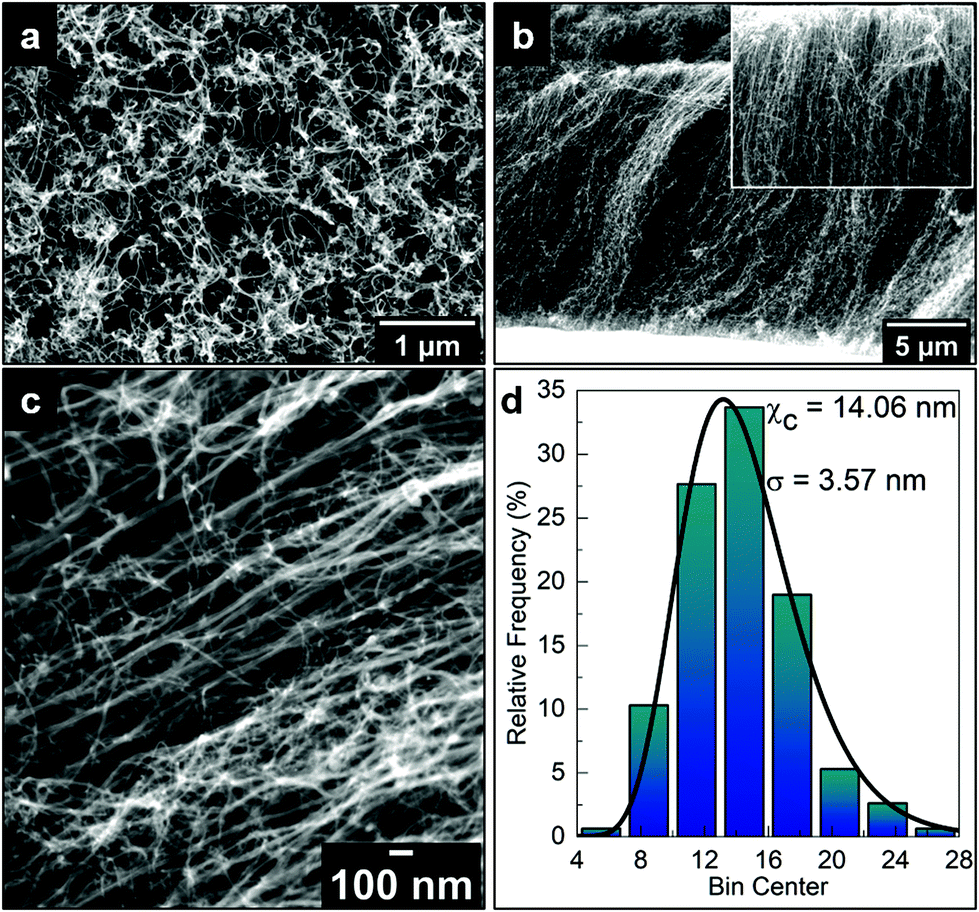 | ||
| Fig. 1 Scanning electron microscopy (SEM) images of the as-grown vertically aligned carbon nanotubes (VA-CNT). (a) Top-view SEM image showing the tips of the CNT “forest”. (b) Side-view SEM image of the VA-CNT showing a height of about to 17 μm. (c) 45° tilt of one of the SEM images used to measure the CNT diameter, whose relative frequency distribution is depicted in (d). (d) From the LogNormal fitting to the distribution, an average diameter of 14.0 nm ± 3.6 nm was obtained. | ||
Fig. 2 shows the SEM image of the ACNTA/PDMS flexible material containing the CNTs transferred from the Si/SiO2 wafer to the PDMS matrix. Bearing in mind the weight of the wafer applying a shear force during drop casting, it is expected that the VA-CNTs will in turn convert to horizontally aligned carbon nanotubes (HA-CNTs) as shown in the top-view SEM image of Fig. 2a. The cross-sectional SEM image shown in Fig. 2b displays two distinguished areas: a top region, showing the CNTs laying down after the casting process; and the bottom region still containing vertically aligned CNTs. The top interfacial region corresponds to the CNTs that were in contact with the Si/SiO2 wafer and the VA-CNTs are in contact with the PDMS. The CNTs in contact with PDMS remained aligned due to densification caused by the PDMS that ascended into the CNTs by capillary forces, as highlighted in the inset of Fig. 2b, where features of the VA-CNTs can be seen embedded in the polymeric matrix (reference Fig. 1b). This effect should be very pronounced, considering both the high cross-sectional contact area and the sorptivity of CNTs.44 The same densification should occur at a lower level in the HA-CNT region after PANI electrodeposition.
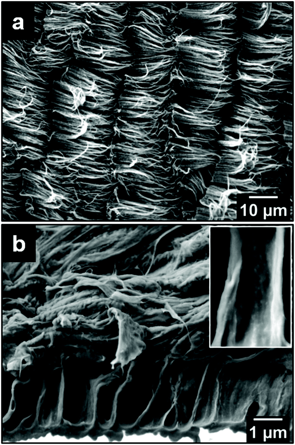 | ||
| Fig. 2 (a) Top-view SEM image of the horizontally aligned carbon nanotubes (HA-CNTs) that were bent during the wafer drop casting process. (b) Cross-sectional SEM image of the flexible electrode showing HA-CNTs on top of vertically aligned carbon nanotubes (VA-CNTs) densified when in contact with the polydimethylsiloxane (PDMS) matrix. PANI is a thin indistinguishable layer spread across the HA-CNTs/air interface. | ||
The structural evaluation of the flexible material was carried out in two steps. Firstly, the micro-Raman laser was focused on the PANI covered region of the sample (marked “ACNTA PANI/PDMS” in Fig. 3b), and next it irradiated the HA-CNTs that were underneath PANI (noted as “ACNTA/PDMS”, black line, and shown in Fig. 3b). The HA-CNTs were exposed after a scotch-tape exfoliation of the superficial PANI layer, in which the latter is visible in the optical image of Fig. 3c. This approach was chosen since the overlapping Raman active peaks of PANI and the CNTs, alongside the low penetration depth of the 532 nm laser into the VA-CNTs, complicate the analysis of the peak convolution and mask the PDMS Raman active peaks from the electrode spectrum (cyan line in Fig. 3a). In addition, the strong presence of peaks related to the PANI and the lacking G′ band of the CNTs were a strong indication that electrodeposited PANI remained on the surface. The PANI Raman spectrum obtained from the material on the scotch-tape (green line) and the PDMS from the opposite surface (orange line) are presented in Fig. 3a as reference. The peaks attributed to the PANI nanostructures correspond to the out of plane ring deformation (about 410 cm−1), ring deformation and silicon vibrations (520 cm−1), quinonoid ring deformation (730 cm−1 and 763 cm−1), benzenoid ring deformation (805 cm−1), C–H deformation (960 cm−1), in-plane bending of the C–H bonds in the semiquinonoid ring (1165 cm−1), stretching of the C–N (1330 cm−1, 1350 cm−1, 1375 cm−1, and C![[double bond, length as m-dash]](https://www.rsc.org/images/entities/char_e001.gif) N at 1475 cm−1), and N–H bending (1520 cm−1).45 Extra peaks in the PANI spectrum (green line) are from the Scotch-tape used in the exfoliation process. The typical peaks for cured PDMS are assigned to the aromatic C–H stretching (3000 cm−1), CH3 symmetric stretching (2890 cm−1), Si–C symmetric stretching (710 cm−1), and Si–O–Si stretching (622 cm−1 and 494 cm−1).46
N at 1475 cm−1), and N–H bending (1520 cm−1).45 Extra peaks in the PANI spectrum (green line) are from the Scotch-tape used in the exfoliation process. The typical peaks for cured PDMS are assigned to the aromatic C–H stretching (3000 cm−1), CH3 symmetric stretching (2890 cm−1), Si–C symmetric stretching (710 cm−1), and Si–O–Si stretching (622 cm−1 and 494 cm−1).46
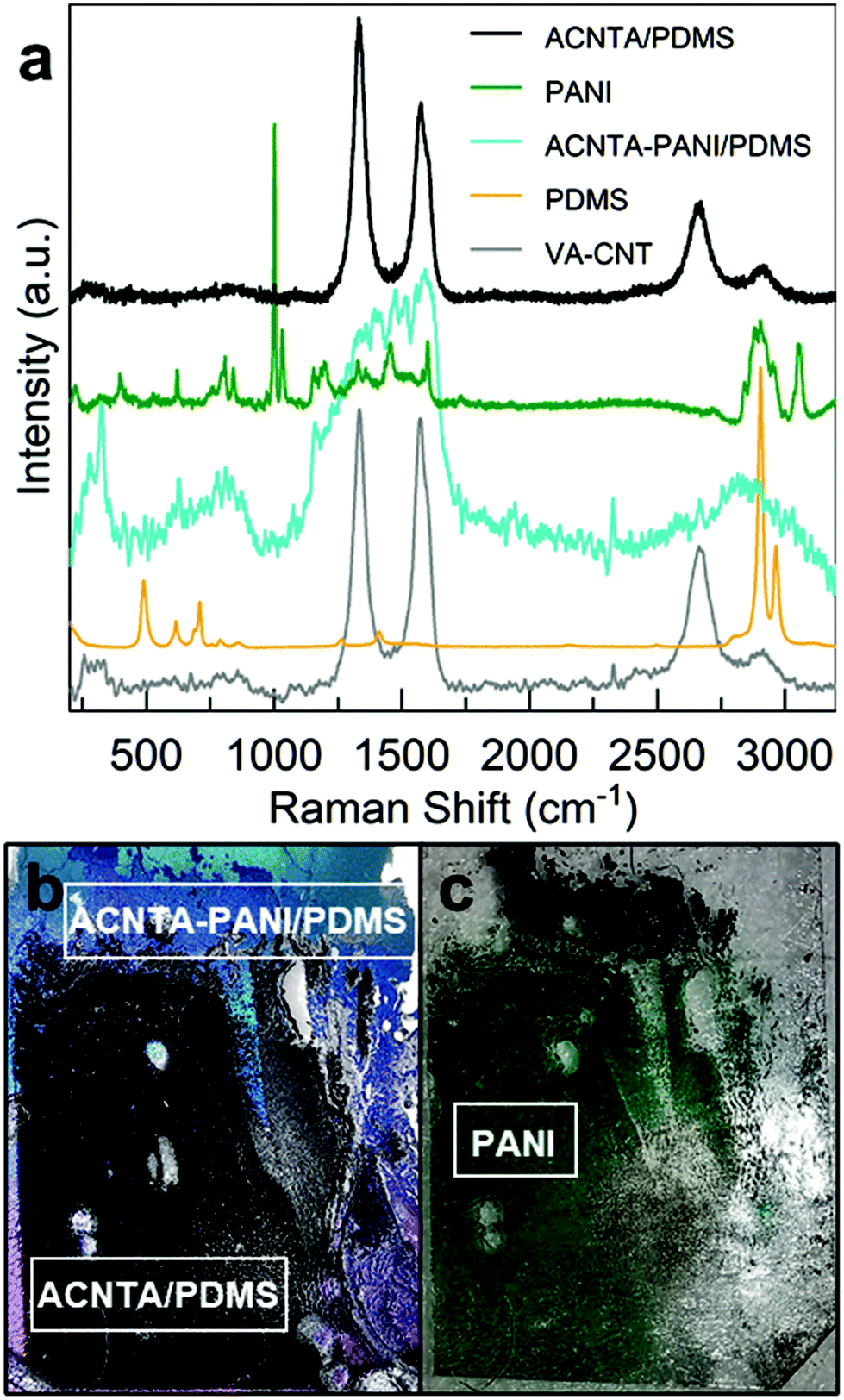 | ||
| Fig. 3 (a) Raman spectra of the flexible electrode (ACNTA-PANI/PDMS, represented in cyan), the horizontally aligned carbon nanotubes (HA-CNTs) underneath the PANI superficial layer (ACNTA/PDMS, black line), and the as-grown CNTs on the Si/SiO2 wafer (CNT, in grey). The PANI and PDMS spectra were added as comparative purposes. (b) The ACNTA-PANI/PDMS label defines the original electrode area, whilst the “ACNTA/PDMS” label identifies the HA-CNTs region underneath the PANI following the scotch-tape exfoliation. (c) PANI exfoliated from the electrode surface. | ||
Raman spectroscopy is a well-known technique used to benchmark CNTs. The quality of the carbon nanotubes can be estimated based on the ratio between the D and G peaks, in which the D peak appears between 1330 and 1360 cm−1 and the G peak can be found at 1580 cm−1, and hence the importance of having to exfoliate the PANI layer masking the peaks prior to this analysis. As shown in Fig. 3a, the as-grown VA-CNTs (grey line) presented an ID/IG ratio of 1.0 ± 0.4, while the ID/IG of the HA-CNTS underneath the PANI layer (black line) was 1.5 ± 0.3. A considerably higher D peak can be a consequence of defects, which as measured by Raman spectroscopy, is any contribution coming from lattice defects (substitution, inclusion, vacancies, or impurities) or amorphous carbon.47 Therefore, we attribute the higher ID/IG ratio of the electrode to the amorphous carbon resulting from the electrodeposition of PANI or possibly to defects introduced during the bending of the CNTs during drop casting, such as kinks on the nanotubes’ walls.
Contact angle measurements (refer to ESI, Fig. S1†) were performed to complement the conclusions drawn from the microscopy and spectroscopy studies. It is observed that the water droplet contact angle of 128.5° for the ACNTA-PANI/PDMS sample is higher than the value observed for ACNTA/PDMS and pure PDMS, being 125.74° and 90.55°, respectively. The lower contact angle measured for the pure PDMS was expected based on the possible hydrogen bonds occurring between water molecules and the oxygen atoms contained in the (–SiO(CH3)2)n monomer, and the higher value of the PDMS/CNTs is another indication that the diffusion of the PDMS was limited to the bottom half of the VA-CNTs (refer Fig. 1b). Following PANI electrodeposition, a slight and non-significant change of about 2% (within instrument experimental error)48 in the contact angle occurred from 125.74° for the ACNTA/PDMS to 128.57° for ACNTA-PANI/PDMS, which can be explained by the PANI diffusion along the CNTs (refer Fig. 3b and c).49,50
Electrochemical results
The electrochemical performance of the ACNTA-PANI/PDMS electrodes was firstly investigated via cyclic voltammetry (CV) and galvanostatic charge/discharge (GCD) measurements with potentials ranging between −0.2 and 0.8 VAg/AgCl. The typical CV profiles measured in the three-electrode configuration are shown in Fig. 4a where two pairs of redox peaks were observed at approximately 0.32 V/−0.06 V and 0.55 V/0.4 V, attributed to leucoemeraldine/emeraldine and emeraldine/pernigraniline transition forms of PANI, respectively, revealing a strong pseudocapacitive behaviour. A reduction of the redox peaks whilst increasing the scan rate can be observed and related to the high-frequency charge diffusion through the inner active sites of the electrodes, minimising redox reactions during the charge and discharge processes.10,51 Moreover, the oxidation peaks shifting positively at higher scan rates are indicative of kinetic limited systems.52 GCD curves (Fig. 4b) exhibited a triangular profile with small deviations from linearity due to pseudocapacitive behaviour of PANI, and quicker charge/discharge with increasing applied current density is typical for SCs as a result of ready-to-transfer charge carriers between the active electrode and the electrolyte.53,54Fig. 4c and Fig. S2† further show the values of areal and gravimetric specific capacitances calculated from the discharge curves over current densities varying from 1 to 3 mA cm−2. The values of gravimetric specific capacitances were calculated based on the mass of PANI electrodeposited on the surface of ACNTA/PDMS. The maximum values of areal and gravimetric specific capacitances were 408 mF cm−2 and 265 F g−1, respectively, at a current density of 1 mA cm−2. Such specific capacitance values are remarkable for flexible/wearable supercapacitors. A comparison of the electrochemical performance of ACNTA-PANI/PDMS measured in a three-electrode configuration with various similar materials reported in previous studies are listed in Table S1.†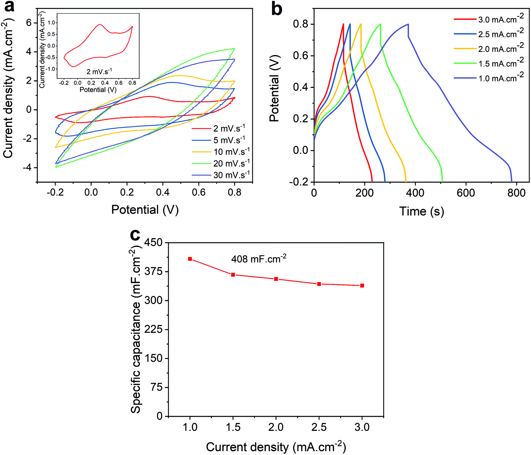 | ||
| Fig. 4 Electrochemical performance of ACNTA-PANI/PDMS measured in a three-electrode configuration. (a) CV curves of the electrodes at different scan rates from 2 to 30 mV s−1. The inset shows the CV curve at a scan rate of 2 mV s−1. (b) GCD curves at different current densities varying from 1 to 3 mA cm−2. (c) Areal specific capacitance calculated from GCD curves. | ||
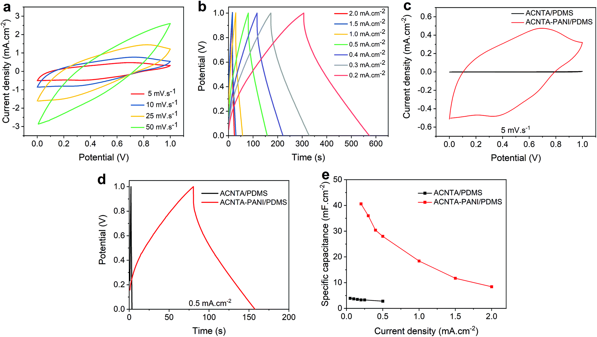
To further explore the electrochemical properties of the ACNTA-PANI/PDMS electrodes as an energy storage device, a flexible symmetric two-electrode supercapacitor was fabricated (inset of Fig. 5d) and studied in an ionic liquid electrolyte. The CV curves of the ACNTA/PDMS and ACNTA-PANI/PDMS structure measured at scan rates varying between 5 and 50 mV s−1 in a potential range of 0–1 V are shown in Fig. S3a† and Fig. 5a, respectively. The ACNTA/PDMS device exhibited the typical rectangular shape regardless of the scan rates as expected from electrical double-layer capacitors. On the other hand, CV curves containing redox peaks from the multiple reduction and oxidation states of PANI points out the existence of a PC behaviour.52,55 Furthermore, with the increase in the scan rate, the oxidation peaks shifted positively (in contrast to the anodic peaks) due to an increase in the internal resistance of the electrodes, deviating from the ideal shape of CV curves.5,56 Additionally, the GCD curves of ACNTA/PDMS and ACNTA-PANI/PDMS at different current densities are shown in Fig. S3b† and Fig. 5b, respectively. Both devices displayed nearly symmetric triangular profiles, revealing high reversibility during charge/discharge processes. ACNTA/PANI presented an ideal linear profile of charge/discharge, evidencing the EDLC behaviour of the CNTs, while the ACNTA-PANI/PDMS sample showed a slight deviation in the triangular shape that confirms the presence of the already pointed-out pseudocapacitive behaviour combined with the EDLC mechanism.5,19,55 Furthermore, Fig. 5c compares the CV curves of ACNTA/PDMS and ACNTA-PANI/PDMS devices at a scan rate of 5 mV s−1. The CV area of ACNTA-PANI/PDMS is remarkably higher than that of ACNTA/PDMS and demonstrates a significant improvement in energy storage properties after PANI electropolymerization on the surface of ACNTAs. This is further confirmed, as shown in Fig. 5d comparing the GCD curves of both samples at a current density of 0.5 mA cm−2, showing the larger charge/discharge time of ACNTA-PANI/PDMS at the same current density caused by higher specific capacitances obtained when PANI is present. This suggests that the presence of PANI directly electrodeposited on the surface of the aligned CNTs produces a composite that enhances the interfacial charge transfer through the electrodes and, therefore, improves the overall electrochemical performance.51,57 The areal specific capacitances were calculated from the GDC measurements and plotted in Fig. 5e. ACNTA-PANI/PDMS delivered a maximum value of 40.6 mF cm−2 at 0.2 mA cm−2, about 24 times higher than ACNTA/PDMS at the same current density. Once again we highligth the charge accumulation increase at the electrode/electrolyte interface due to PANI redox reactions and the synergetic effect between PANI and ACNTAs as numerous conductive pathways that allow fast ion diffusion through the electrodes.54,55,58
 | ||
| Fig. 5 Electrochemical performance of symmetric two-electrode supercapacitors. (a) CV curves of ACNTA-PANI/PDMS at scan rates varying between 5 and 50 mV s−1. (b) GCD curves at different current densities. (c) CV curves of ACNTA/PDMS and ACNTA-PANI/PDMS at a scan rate of 5 mV s−1. (d) GCD curves of ACNTA/PDMS and ACNTA-PANI/PDMS at 0.5 mA cm−2. (e) Areal specific capacitances calculated for different current densities. | ||
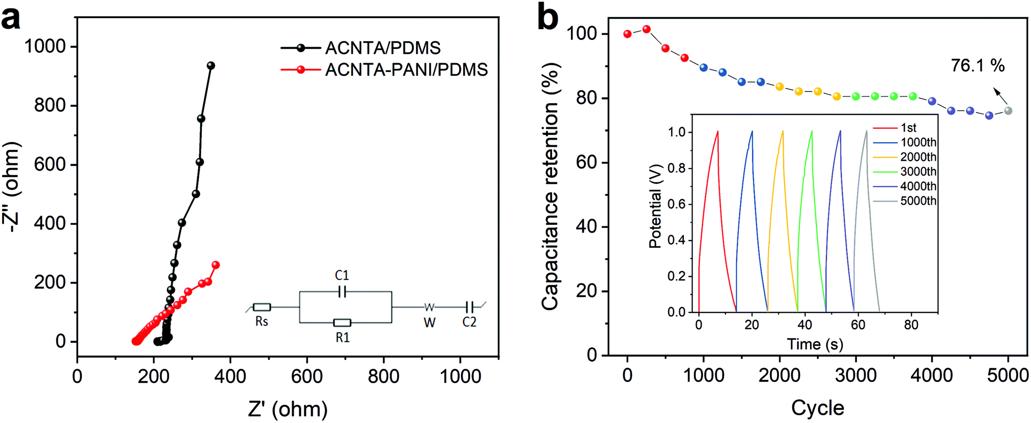
EIS measurements were further performed and Fig. 6a shows the Nyquist plot of ACNTA/PDMS and ACNTA-PANI/PDMS devices. The experimental data were adjusted to the equivalent circuit exhibited in the inset of Fig. 6a. The Rs denote the internal resistance of the electrodes, while the C1/R1 elements connected in parallel represents the electrochemical reaction impedance. The W denotes the Warburg impedance resulting from the frequency dependence of ionic diffusion through the electrode/electrolyte interface and C2 corresponds to the intercalation capacitance, which can be associated with the pseudocapacitance of the devices.54,59 The parameters obtained from the equivalent electric circuit are described in detail in Table S2.† The real axis intercept values at high frequencies denote the internal resistance of the electrodes and the contact resistance between the electrodes and electrolyte (Rs).53,60 The Rs values were 214.8 and 153.3 ohm cm−2 for the ACNTA/PDMS and ACNTA-PANI/PDMS device, respectively, suggesting that PANI provided a good electrical network within the ACNTAs, which facilitated charge transfer through the electrodes, and consequently modified the Rs value. The C1 values were approximately the same for the two electrodes, 8.35 mF cm−2 for ACNTA-PANI/PDMS and 7.00 mF cm−2 for ACNTA/PDMS, indicating similar contribution of the double-layer capacitance for both samples. Furthermore, the ACNTA-PANI/PDMS electrode displayed a R1 value approximately 3 times smaller than ACNTA/PDMS (72.5 ohm cm−2 and 209.7 ohm cm−2, respectively), indicating a lower charge transfer resistance for the device containing PANI. Finally, the C2 values represents the contribution of the pseudocapacitance mechanism for each sample, reaching 1.04 mF cm−2 for ACNTA/PDMS and 20.23 mF cm−2 for ACNTA-PANI/PDMS, which is in good agreement with the previous results.
 | ||
| Fig. 6 Electrochemical performance of symmetric two-electrode supercapacitors. (a) EIS curve of ACNTA-PANI/PDMS at frequencies varying between 10−1 and 105 Hz; the inset shows the equivalent circuit used for fitting the experimental data. (b) GCD stability of ACNTA-PANI/PDMS in a potential range between 0 and 1 V for 5000 cycles. | ||
Long-term cycling stability (i.e., capacitance retention) was evaluated after 5000 charge/discharge cycles of the ACNTA-PANI/PDMS device, as shown in Fig. 6b. The capacitance gradually increased during the first 250 cycles, suggesting an improvement of surface wettability and activation process of the electrodes.51,61 After 5000 cycles, the capacitance retention was partially stabilized at 76.1%.
The working voltage of supercapacitors is an important parameter that controls their electrochemical properties and is directly related to the amount of energy that the device is capable of storing. Aiming to improve the energy density stored in our ACNTA-PANI/PDMS device, CV and GCD measurements were performed at a working potential of 2 V and different scan rates varying between 5 and 50 mV s−1, as shown in the CV curves of Fig. 7a. The CV curves display characteristic prominent redox peaks during positive and negative sweeps, corroborating the existence of deeper reactions at wider potentials, which is a commonly reported behaviour.62,63 Thus, a slight deviation in the CV shape is expected as the scan rate increases due to the increase in the current density. Accordingly, Fig. 7b displays the GCD profiles of the ACNTA-PANI/PDMS device at a working voltage of 2 V tested at different current densities. As observed in the CV measurements, the GCD results reveal the presence of a stronger PC behaviour of PANI appearing for wider potentials as evidenced by the distortions in the charge/discharge profiles.5,52 A small voltage drop (IR drop) in the beginning of the discharge curves was noticed in all curves and attributted to the internal resistance of the electrodes. Moreover, the discharge curves exhibited two well pronounced stages with a fast linear discharge followed by a much longer discharge time as a characteristic of a PC mechanism.2
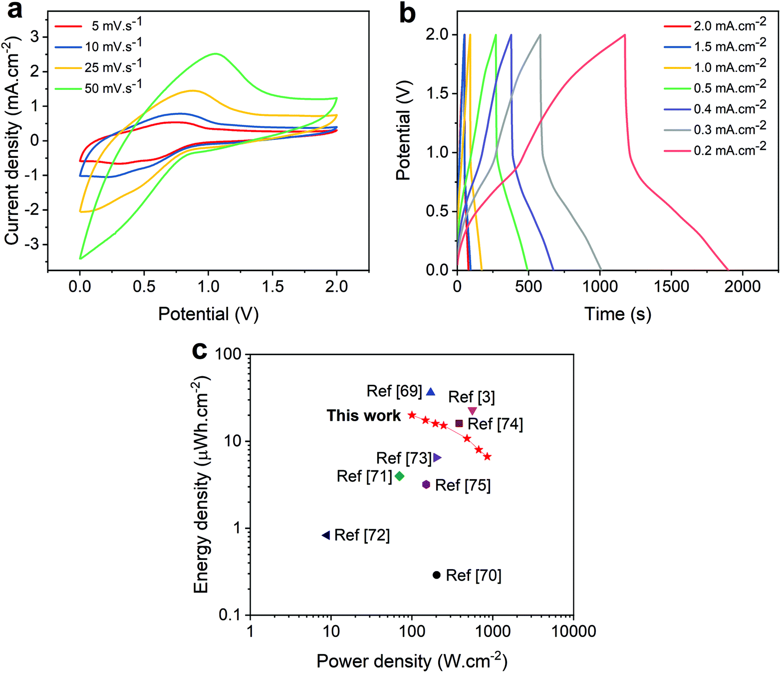 | ||
| Fig. 7 Electrochemical properties of ACNTA-PANI/PDMS over different potential ranges varying from 0 to 2 V. (a) CV curves at different scan rates. (b) GCD curves at different current densities. (c) Ragone plot comparing the values of areal energy and power density of this work with similar flexible supercapacitors described in the literature.3,69–75 | ||
A Ragone plot containing the values of areal energy and power densities calculated from GCD measurements is plotted in Fig. 7c. Since the values of energy and power densities are proportional to the square of the voltage (see eqn (5) and (6) available in the ESI†), one should expect an increase in the quantity of energy stored with a broader voltage range. When measured at a potential range beetween 0 and 2 V, the ACNTA-PANI/PDMS device delivered a maximum specific energy density of 20 μW h cm−2 at a power density of 100 μW cm−2 but maintained an energy density of 6.7 μW h cm−2 when the power density increased to 856 μW cm−2, revealing an excellent performance, as confirmed by the comparison with other flexible SCs (Fig. 7c). Thus, the gravimetric energy and power densities calculated based on the PANI mass are shown in the Ragone plot displayed in Fig. S4.† A high energy density of 25.5 W h kg−1 was obtained at a power density of 126.6 W kg−1, maintaining 8.3 W h kg−1 when the power density increased to 1071 W kg−1. All these results suggest that the high number of active sites derived from the multiple oxidation states of PANI improved the amount of charges accumulated in the electrodes.19,31,54,64
The flexibility of the ACNTA-PANI/PDMS device was further investigated by comparing the electrochemical performance under different bending angles. Fig. 8a displays the CV curves at a scan rate of 25 mV s−1 under bending angles of 0°, 60°, 90° and 120°. The CV curves presented nearly similar profiles even when the bending angle increased up to 120°, revealing that the device preserves great capacitive behaviour when deformed. The normalized specific capacitances were calculated according to the CV curves as the bending angles increased from 0° to 120°, and the results are shown in Fig. 8b. A decrease in the values of capacitance with further increase in the bending angle was observed, but a retention of 80.4% when bent to 120° confirms the viability of using ACNTA/PDMS as a platform for stretchable energy storage devices.
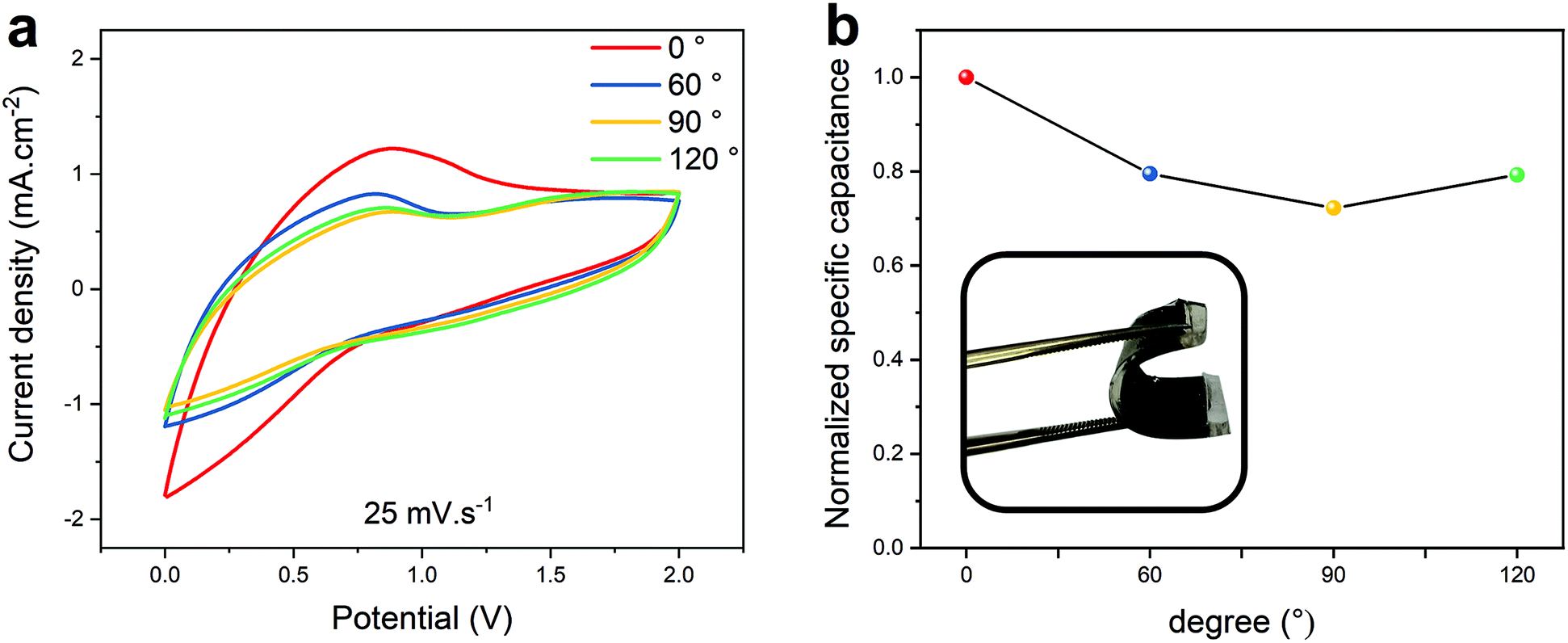 | ||
| Fig. 8 Performance of the ACNTA-PANI/PDMS device under different bending angles. (a) CV curves at 25 mV s−1. (b) Normalized specific capacitance calculated from the CV curves over the bent angle. The inset illustrates the flexibility of the devices under different angles. | ||
Conclusions
This work described the fabrication of a high-performance flexible supercapacitor based on polyaniline-coated ACNTA/PDMS. Aligned CNTs were transferred from a Si wafer to a PDMS substrate, providing a densely compacted CNT “forest” and granting thermal and chemical stability in addition to great flexibility. PANI was directly electropolymerized on the surface of the aligned CNTs, which resulted in a structure with remarkable electrochemical properties. The abundant active sites and multiple oxidation states of PANI promoted a significant enhancement in the energy storage properties of the ACNTA-PANI/PDMS electrodes, which delivered a maximum areal specific capacitance of 408 mF cm−2 at 1 mA cm−2. Moreover, the symmetric two-electrode flexible device displayed a high energy density of 20 μW h cm−2 (25.5 W h kg−1) at a power density of 100 μW kg−1 (126.6 W kg−1), which is among the best reported for flexible devices. Thus, the device can maintain 80.4% of its electrochemical properties when bent at 120°. Considering the significant findings of this study, the ACNTA-PANI/PDMS electrodes are a promising candidate for future flexible electronics, presenting outstanding achievements combined with facile and low-cost fabrication with few processing steps. A truly flexible technology which will bridge the requirements of energy and power for future IoT devices is demonstrated in this paper.Experimental
Growth of vertically aligned carbon nanotubes
Carbon nanotubes (CNTs) were deposited via the photothermal chemical vapour deposition method (PTCVD), as described elsewhere.43,65,66 In brief, the PTCVD system is a complementary metal–oxide–semiconductor (CMOS) compatible, low-temperature CNT growth method which employs an optical heat source to efficiently couple the high optical energy and focus it at the catalyst front only whilst the substrate is being water cooled continuously. This allows achieving up to 300 °C temperature gradients between the catalyst front and the substrate. CNT deposition was performed on a full 4-inch silicon (Si) wafer with 300 nm native oxide (SiO2). A 3 nm iron (Fe0) catalyst layer was sputtered on top of a 10 nm aluminum (Al0) co-catalyst interlayer to prevent the catalyst from coalescence and increase the CNT density. The PTCVD system was operated at around 400–420 °C substrate temperature, measured using a bulk pyrometer.67 The Fe0 catalyst was activated for 5 min under 100 sccm H2, immediately followed by 5 min growth under 100 sccm H2 and 25 sccm (acetylene) C2H2 at 5 torr chamber pressure. After 5 min, C2H2 supply was cut-off, hydrogen (H2) was allowed to flowing into the chamber with the optical light on for an extra minute to avoid amorphous carbon built-up on the tip of the CNTs. The chamber was cooled down to room temperature and purged twice with nitrogen (N2) before the substrates were removed.Preparation of ACNTA-PANI/PDMS
A schematic illustration of the processes employed during electrode fabrication is shown in Fig. S5.† A solution was prepared by mixing the polydimethylsiloxane (PDMS) base and its curing agent (Dow Chemical Company) with a mass ratio of 10![[thin space (1/6-em)]](https://www.rsc.org/images/entities/char_2009.gif) :1, and degassed under 10−2 mbar for 30 min to prevent bubble formation. After holding the PDMS at 70 °C for 3 h, the vertically aligned carbon nanotubes (VA-CNT) previously grown on the Si wafer was dropcast facing the partially cured PDMS. At the end of the curing process, the Si wafer was pulled, leaving behind the aligned CNTs (ACNTA) which were then attached to the PDMS, since the adhesion of ACNTA/PDMS is stronger than that of the VA-CNTs/Si wafer. Finally, ACNTA/PDMS was coated with a layer of polyaniline via electropolymerization. PANI was electropolymerized on the surface of ACNTA/PDMS through cyclic voltammetry (CV) in a three-electrode configuration, using ACNTA/PDMS as the working electrode, platinum as the counter electrode and Ag/AgCl (saturated with KCl) as the reference electrode. The electrode array was submerged in a solution containing 0.5 mol L−1 aniline (Dinâmica Química Contemporânea) and 0.5 mol L−1 H2SO4 (Êxodo Científica). The electropolymerization was initiated with one cycle in the potential range between 0 and 1.4 VAg/AgCl, followed by 10 cycles in the potential range between 0 and 0.8 VAg/AgCl, at a scan rate of 5 mV s−1. Finally, the fabricated ACNTA-PANI/PDMS electrodes were rinsed with distilled water and left to dry for 12 h.
:1, and degassed under 10−2 mbar for 30 min to prevent bubble formation. After holding the PDMS at 70 °C for 3 h, the vertically aligned carbon nanotubes (VA-CNT) previously grown on the Si wafer was dropcast facing the partially cured PDMS. At the end of the curing process, the Si wafer was pulled, leaving behind the aligned CNTs (ACNTA) which were then attached to the PDMS, since the adhesion of ACNTA/PDMS is stronger than that of the VA-CNTs/Si wafer. Finally, ACNTA/PDMS was coated with a layer of polyaniline via electropolymerization. PANI was electropolymerized on the surface of ACNTA/PDMS through cyclic voltammetry (CV) in a three-electrode configuration, using ACNTA/PDMS as the working electrode, platinum as the counter electrode and Ag/AgCl (saturated with KCl) as the reference electrode. The electrode array was submerged in a solution containing 0.5 mol L−1 aniline (Dinâmica Química Contemporânea) and 0.5 mol L−1 H2SO4 (Êxodo Científica). The electropolymerization was initiated with one cycle in the potential range between 0 and 1.4 VAg/AgCl, followed by 10 cycles in the potential range between 0 and 0.8 VAg/AgCl, at a scan rate of 5 mV s−1. Finally, the fabricated ACNTA-PANI/PDMS electrodes were rinsed with distilled water and left to dry for 12 h.
Characterisation
The morphology of the as-grown VA-CNTs, as well as the ACNTA-PANI/PDMS flexible electrodes was analysed using a scanning electron microscope (SEM), Tescan MIRA II. The VA-CNTs on the silicon/silicon dioxide (Si/SiO2) wafer were inspected using a 0.20 nA electron beam operated at 30 keV, ensuring a spot size lower than 3.8 nm. The diameter of the CNTs were measured using the ImageJ software and its average diameter was obtained after a LogNormal fit to the relative frequency distribution. In order to verify the alignment of the aCNTs following the casting of the Si wafer on the mildly cured PDMS, the sample was cut with a N°11 scalpel blade and mounted on a 45° tilted stub. The stage tilt (up to 35°) allowed us to verify its cross-section region and also to obtain top-view SEM images, both using a 0.20 nA electron beam accelerated at 5 keV which results in a spot size of about 8 nm. The lower energy and the in-beam secondary electron detector allowed the prevention of charging in the PDMS and to obtain more details of the material surface, respectively.Structural characterisation was carried out using micro-Raman spectroscopy, with a laser excitation of 532 nm. The 50× objective lens and the filter resulted in a spot size of 5 μm and a power below 10 mW μm−2. The ratio between the D and G peaks intensity (ID and IG, respectively) benchmarked the quality of the VA-CNTs before and after being converted into a capacitor electrode, and the uncertainty related to the analysis was calculated based on 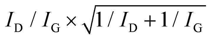 .68
.68
The D and G peak intensities were obtained via Lorentzian curve fittings. PDMS and polyaniline (PANI) were also characterised. The wettability of the materials was checked by contact angle measurements carried out under ambient conditions using an optical tensiometer, Theta Lite TL100, where a drop of distilled water (8 μL) was dropped onto the material surface whilst recording with a digital camera. The images were analysed using Oneattension software.
Electrochemical measurements
To evaluate the electrochemical performance of the electrodes, firstly tests in three-electrode configuration were performed in H2SO4 1 mol L−1 electrolyte, with ACNTA-PANI/PDMS as the working electrode, and Pt mesh and Ag/AgCl (KCl 3 mol L−1) as the counter and reference electrodes, respectively. CV and GCD measurements were conducted in the potential range between −0.2 and 0.8 VAg/AgCl at various scan rates and at different current densities, respectively. To further examine the ACNTA-PANI/PDMS material, a flexible two-electrode supercapacitor was fabricated and tested in an ionic liquid electrolyte (1-butyl 3-methyl imidazolium tetrafluoroborate [BMIM][BF4]). The device was assembled by sandwiching two ACNTA-PANI/PDMS electrodes, using quantitative filter paper (JP40, average porosity of 25 μm) as a separator. An illustration of the supercapacitor assembly is shown in Fig. S6.† CV and GCD tests were performed in a working potential range between 0 and 1 V. Electrochemical impedance spectroscopy (EIS) was performed from 0.1 to 100000 Hz, with an amplitude of 0.005 V referred to the open circuit potential. Long-term cycling stability was assessed according to GCD in a potential range between 0 and 1 V for 5000 cycles. Tests were also performed in a wider voltage range (0–2 V) to improve the energy density stored. Furthermore, CV tests varying the bending angle (0° to 120°) were also performed, as shown in Fig. S7.† The electrochemical tests were performed in a programmable sourcemeter (Keithley – 2651A), a potentiostat (Metrohm Autolab, PGSTAT302 N) and another potentiostat (IVIUM – Compactstat). For further information on how areal and gravimetric specific capacitances, energy, and power densities were calculated, refer to the supplementary material.
Author contributions
All authors contributed significantly to the manuscript, as described: R. D. C. B., G. K. M. and M. G. M. conceived the idea, elaborated the methodology, fabricated the materials, designed and performed the experiments and wrote the paper; M. O. T. elaborated the methodology, helped with the fabrication of materials and wrote the paper; L. S. R. and V. G. contributed to the project design, collected and analyzed the data; J. H. A. and R. A. supervised the project and performed data curation; N. L. V. C. and S. R. P. S. conceived the idea and supervised the project. All authors contributed to the discussion and revised the manuscript prior to submission.Conflicts of interest
The authors declare no conflict of interest.Acknowledgements
We acknowledge the funding support from the Coordenação de Aperfeiçoamento de Pessoal de Nível Superior (CAPES – finance code 001/process number print 88887.310585/2018-0), Fundação de Amparo à Pesquisa do Estado do Rio Grande do Sul (Fapergs/PqG 2017 17/2551-0001157-0), Conselho Nacional de Desenvolvimento Científico e Tecnológico (CNPq) and the University of Surrey acknowledges support from the Brazilian Government FAPESP BEPE and SPRINT Programme for conducting this work.Notes and references
- S. R. P. Silva, Energy Environ. Mater., 2021, 4, 497–499 CrossRef.
- Y. Xiao, Y. Liu, F. Liu, P. Han and G. Qin, J. Alloys Compd., 2020, 813, 152089 CrossRef CAS.
- J. Ren, R. P. Ren and Y. K. Lv, Chem. Eng. J., 2018, 349, 111–118 CrossRef CAS.
- W. Wang, L. Lu, Y. Xie, X. Mei, Y. Tang, W. Wu and R. Liang, Appl. Surf. Sci., 2020, 504, 144487 CrossRef CAS.
- D. Liu, P. Du, W. Wei, H. Wang, Q. Wang and P. Liu, Electrochim. Acta, 2017, 233, 201–209 CrossRef CAS.
- J. Yu, W. Lu, S. Pei, K. Gong, L. Wang, L. Meng, Y. Huang, J. P. Smith, K. S. Booksh, Q. Li, J. H. Byun, Y. Oh, Y. Yan and T. W. Chou, ACS Nano, 2016, 10, 5204–5211 CrossRef CAS PubMed.
- X. Chen, H. Lin, P. Chen, G. Guan, J. Deng and H. Peng, Adv. Mater., 2014, 26, 4444–4449 CrossRef CAS PubMed.
- R. Zhang, J. Ding, C. Liu and E. H. Yang, ACS Appl. Energy Mater., 2018, 1, 2048–2055 CrossRef CAS.
- Q. Jiang, N. Kurra, M. Alhabeb, Y. Gogotsi and H. N. Alshareef, Adv. Energy Mater., 2018, 8, 1–10 Search PubMed.
- H. Luo, J. Dong, Y. Zhang, G. Li, R. Guo, G. Zuo, M. Ye, Z. Wang, Z. Yang and Y. Wan, Chem. Eng. J., 2018, 334, 1148–1158 CrossRef CAS.
- W. Chen, R. B. Rakhi and H. N. Alshareef, J. Mater. Chem. A, 2013, 1, 3315–3324 RSC.
- W. Fan, C. Zhang, W. W. Tjiu, K. P. Pramoda, C. He and T. Liu, ACS Appl. Mater. Interfaces, 2013, 5, 3382–3391 CrossRef CAS PubMed.
- T. Lv, Y. Yao, N. Li and T. Chen, Angew. Chem., Int. Ed., 2016, 55, 9191–9195 CrossRef CAS PubMed.
- R. Zhang, J. Ding, C. Liu and E. H. Yang, Advanced Materials: TechConnect Briefs 2017, 2017, 1, 44–47 Search PubMed.
- M. Saghafi, M. Mahmoodian, S. A. Hosseini, A. Abdollahi and S. Mohajerzadeh, Electrochim. Acta, 2018, 283, 1450–1459 CrossRef CAS.
- S. Hussain, E. Kovacevic, R. Amade, J. Berndt, C. Pattyn, A. Dias, C. Boulmer-Leborgne, M. R. Ammar and E. Bertran-Serra, Electrochim. Acta, 2018, 268, 218–225 CrossRef CAS.
- V. H. R. De Souza, M. M. Oliveira and A. J. G. Zarbin, J. Power Sources, 2014, 260, 34–42 CrossRef.
- G. K. Maron, J. H. Alano, B. da Silveira Noremberg, L. da Silva Rodrigues, V. Stolojan, S. R. P. Silva and N. L. V. Carreño, J. Alloys Compd., 2020, 836, 155408 CrossRef CAS.
- D. D. Potphode, P. Sivaraman, S. P. Mishra and M. Patri, Electrochim. Acta, 2015, 155, 402–410 CrossRef CAS.
- M.-S. Balogun, W. Qiu, W. Wang, P. Fang, X. Lu and Y. Tong, J. Mater. Chem. A, 2015, 3, 1364–1387 RSC.
- R. Adalati, A. Kumar, M. Sharma, P. Tiwari and R. Chandra, Appl. Phys. Lett., 2020, 117, 123904 CrossRef CAS.
- R. Adalati, A. Kumar, Y. Kumar and R. Chandra, Energy Technol., 2020, 8, 2000466 CrossRef CAS.
- M. I. A. Abdel Maksoud, R. A. Fahim, A. E. Shalan, M. Abd Elkodous, S. O. Olojede, A. I. Osman, C. Farrell, H. Ala'a, A. S. Awed and A. H. Ashour, Environ. Chem. Lett., 2020, 1–65 Search PubMed.
- S. Khalid, Y. Khan, E. Ahmed, S. Nawaz, N. R. Khalid and W. Ahmed, in Emerging Nanotechnologies for Renewable Energy, Elsevier, 2021, pp. 407–445 Search PubMed.
- S. Hussain, R. Amade and E. Bertran, Mater. Chem. Phys., 2014, 148, 914–922 CrossRef CAS.
- W. K. Chee, H. N. Lim, I. Harrison, K. F. Chong, Z. Zainal, C. H. Ng and N. M. Huang, Electrochim. Acta, 2015, 157, 88–94 CrossRef CAS.
- S. J. Paul, I. Sharma, I. Elizabeth, B. Gahtori, R. Manikandan, S. S. Titus, P. Chandra and B. K. Gupta, ACS Appl. Mater. Interfaces, 2020, 12, 16946–16958 CrossRef CAS PubMed.
- C. Lim, Y. Shin, S. Hong, S. Lee and D. H. Kim, Adv. Mater. Interfaces, 2020, 7, 1–8 Search PubMed.
- M. Ramadan, A. M. Abdellah, S. G. Mohamed and N. K. Allam, Sci. Rep., 2018, 8, 1–8 Search PubMed.
- M. Li, M. F. El-Kady, J. Y. Hwang, M. D. Kowal, K. Marsh, H. Wang, Z. Zhao and R. B. Kaner, Nano Res., 2018, 11, 2836–2846 CrossRef CAS.
- S. Y. Lee, J. Il Kim and S. J. Park, Energy, 2014, 78, 298–303 CrossRef CAS.
- S. B. Yoon, E. H. Yoon and K. B. Kim, J. Power Sources, 2011, 196, 10791–10797 CrossRef CAS.
- V. Mottaghitalab, B. Xi, G. M. Spinks and G. G. Wallace, Synth. Met., 2006, 156, 796–803 CrossRef CAS.
- S. R. Mangisetti, M. Kamaraj and S. Ramaprabhu, Electrochim. Acta, 2019, 305, 264–277 CrossRef CAS.
- A. M. White and R. C. T. Slade, Electrochim. Acta, 2004, 49, 861–865 CrossRef CAS.
- H. Zhang, Y. Liu, C. Yang, L. Xiang, Y. Hu and L. Peng, Adv. Mater., 2018, 30, 1805408 CrossRef PubMed.
- D. Janas and K. K. Koziol, Nanoscale, 2014, 6, 3037–3045 RSC.
- E. J. Park, K.-D. Kim, H. S. Yoon, M.-G. Jeong, D. H. Kim, D. C. Lim, Y. H. Kim and Y. D. Kim, RSC Adv., 2014, 4, 30368–30374 RSC.
- C. Choi, M. K. Choi, S. Liu, M. S. Kim, O. K. Park, C. Im, J. Kim, X. Qin, G. J. Lee, K. W. Cho, M. Kim, E. Joh, J. Lee, D. Son, S. H. Kwon, N. L. Jeon, Y. M. Song, N. Lu and D. H. Kim, Nat. Commun., 2017, 8(1) DOI:10.1038/s41467-017-01824-6.
- M. Amjadi, K. U. Kyung, I. Park and M. Sitti, Adv. Funct. Mater., 2016, 26, 1678–1698 CrossRef CAS.
- M. Xue, F. Li, J. Zhu, H. Song, M. Zhang and T. Cao, Adv. Funct. Mater., 2012, 22, 1284–1290 CrossRef CAS.
- A. Khosrozadeh, G. Singh, Q. Wang, G. Luo and M. Xing, J. Mater. Chem. A, 2018, 6, 21064–21077 RSC.
- M. O. Tas, M. A. Baker, M. G. Masteghin, J. Bentz, K. Boxshall and V. Stolojan, ACS Appl. Mater. Interfaces, 2019, 11, 39560–39573 CrossRef CAS PubMed.
- D. Łukawski, F. Lisiecki and A. Dudkowiak, Fibers Polym., 2018, 19, 524–530 CrossRef.
- M. Trchová, Z. Morávková, M. Bláha and J. Stejskal, Electrochim. Acta, 2014, 122, 28–38 CrossRef.
- D. Cai, A. Neyer, R. Kuckuk and H. M. Heise, J. Mol. Struct., 2010, 976, 274–281 CrossRef CAS.
- K. Sato, R. Saito, Y. Oyama, J. Jiang, L. G. Cancado, M. A. Pimenta, A. Jorio, G. G. Samsonidze, G. Dresselhaus and M. S. Dresselhaus, Chem. Phys. Lett., 2006, 427, 117–121 CrossRef CAS.
- S. Chen, Y. Chen, X. Liu, S. Shen and X. Wang, Int. J. Energy Clean Environ., 2018, 19, 105–117 CrossRef.
- J. Bae, Y. Hwang, S. J. Park, J.-H. Ha, H. J. Kim, A. Jang, J. An, C.-S. Lee and S.-H. Park, Polymers, 2018, 10, 951 CrossRef PubMed.
- W. Zhai, Q. Xia, K. Zhou, X. Yue, M. Ren, G. Zheng, K. Dai, C. Liu and C. Shen, Chem. Eng. J., 2019, 372, 373–382 CrossRef CAS.
- Q. Liu, S. Jing, S. Wang, H. Zhuo, L. Zhong, X. Peng and R. Sun, J. Mater. Chem. A, 2016, 4, 13352–13362 RSC.
- A. Stott, M. O. Tas, E. Y. Matsubara, M. G. Masteghin, J. M. Rosolen, R. A. Sporea and S. R. P. Silva, Energy Environ. Mater., 2020, 3, 389–397 CrossRef CAS.
- V. Gehrke, G. K. Maron, L. da Silva Rodrigues, J. H. Alano, C. M. P. de Pereira, M. O. Orlandi and N. L. V. Carreño, Mater. Today Commun., 2020, 101779 Search PubMed.
- G. Wu, P. Tan, D. Wang, Z. Li, L. Peng, Y. Hu, C. Wang, W. Zhu, S. Chen and W. Chen, Sci. Rep., 2017, 7, 1–8 CrossRef PubMed.
- H. Lin, L. Li, J. Ren, Z. Cai, L. Qiu, Z. Yang and H. Peng, Sci. Rep., 2013, 3, 1–6 Search PubMed.
- L. Zhang, D. Huang, N. Hu, C. Yang, M. Li, H. Wei, Z. Yang, Y. Su and Y. Zhang, J. Power Sources, 2017, 342, 1–8 CrossRef CAS.
- K. Jost, D. Stenger, C. R. Perez, J. K. McDonough, K. Lian, Y. Gogotsi and G. Dion, Energy Environ. Sci., 2013, 6, 2698–2705 RSC.
- S. A. El-Khodary, G. M. El-Enany, M. El-Okr and M. Ibrahim, Synth. Met., 2017, 233, 41–51 CrossRef CAS.
- H. Wang, J. Lin and Z. X. Shen, J. Sci.: Adv. Mater. Devices, 2016, 1, 225–255 Search PubMed.
- T. Chen, H. Peng, M. Durstock and L. Dai, Sci. Rep., 2014, 4, 1–7 CrossRef.
- K. Wang, Q. Meng, Y. Zhang, Z. Wei and M. Miao, Adv. Mater., 2013, 25, 1494–1498 CrossRef CAS PubMed.
- M. Gao, X. Wu, H. Qiu, Q. Zhang, K. Huang, S. Feng, Y. Yang, T. Wang, B. Zhao and Z. Liu, RSC Adv., 2018, 8, 20661–20668 RSC.
- S. Lehtimäki, A. Railanmaa, J. Keskinen, M. Kujala, S. Tuukkanen and D. Lupo, Sci. Rep., 2017, 7, 1–9 CrossRef PubMed.
- M. Yu, Y. Zhang, Y. Zeng, M. S. Balogun, K. Mai, Z. Zhang, X. Lu and Y. Tong, Adv. Mater., 2014, 26, 4724–4729 CrossRef CAS PubMed.
- M. Ahmad, J. V. Anguita, V. Stolojan, T. Corless, J. Chen, J. D. Carey and S. R. P. Silva, Adv. Funct. Mater., 2015, 25, 4419–4429 CrossRef CAS.
- J.-S. Chen, V. Stolojan and S. R. P. Silva, Carbon, 2015, 84, 409–418 CrossRef CAS.
- M. O. Tas, M. A. Baker, V. Musaramthota, H. Uppal, M. G. Masteghin, J. Bentz, K. Boxshall and V. Stolojan, Carbon, 2019, 150, 117–127 CrossRef CAS.
- M. G. Masteghin, M. Ahmad, M. O. Tas, C. T. G. Smith, V. Stolojan, D. C. Cox and S. R. P. Silva, Appl. Phys. Lett., 2020, 116, 103101 CrossRef CAS.
- X. Liang, L. Zhao, Q. Wang, Y. Ma and D. Zhang, Nanoscale, 2018, 10, 22329–22334 RSC.
- P. Avasthi, A. Kumar and V. Balakrishnan, ACS Appl. Nano Mater., 2019, 2, 1484–1495 CrossRef CAS.
- L. Li, Z. Lou, W. Han, D. Chen, K. Jiang and G. Shen, Adv. Mater. Technol., 2017, 2(3), 1600282 CrossRef.
- Y. Zhu, N. Li, T. Lv, Y. Yao, H. Peng, J. Shi, S. Cao and T. Chen, J. Mater. Chem. A, 2018, 6, 941–947 RSC.
- H. Park, C. Song, S. W. Jin, H. Lee, K. Keum, Y. H. Lee, G. Lee, Y. R. Jeong and J. S. Ha, Nano Energy, 2021, 83, 105837 CrossRef CAS.
- V. K. A. Muniraj, R. Boukherroub and M. V. Shelke, ACS Sustainable Chem. Eng., 2020, 8, 6433–6441 CrossRef CAS.
- A. P. M. Udayan, O. Sadak and S. Gunasekaran, ACS Appl. Energy Mater., 2020, 3, 12368–12377 CrossRef CAS.
Footnote |
| † Electronic supplementary information (ESI) available. See DOI: 10.1039/d1nr06914d |
| This journal is © The Royal Society of Chemistry 2022 |