
Enhancing the performance of n-i-p perovskite solar cells by introducing hydroxyethylpiperazine ethane sulfonic acid for interfacial adjustment†
Putao
Zhang
 ,
Yiming
Chen
,
Shenghan
Wu
,
Xiaohui
Li
,
Meiyue
Liu
and
Shengjun
Li
*
,
Yiming
Chen
,
Shenghan
Wu
,
Xiaohui
Li
,
Meiyue
Liu
and
Shengjun
Li
*
Key Laboratory of Photovoltaic Materials, Henan University, Henan, Kaifeng 475004, China. E-mail: lishengjun@henu.edu.cn
First published on 2nd November 2021
Abstract
Although the power conversion efficiency (PCE) of perovskite solar cells (PSCs) has improved greatly in recent years, the challenges of efficiency and stability still need to be overcome before these solar cells can be used in commercial applications. Here, a weak acid buffer, hydroxyethyl piperazine ethane sulfonic acid (HEPES), is used to passivate the interface of an SnO2 electron transport layer (ETL) and a photoactive layer in n-i-p solar cells. The device efficiency based on a SnO2/HEPES ETL reaches 20.22%, which is 9.7% higher than that of the control (18.43%), and the device stability is also significantly improved. The improvement in the device performance is mainly due to the introduction of the HEPES interface layer to adjust the interface energy level, which also improves the crystallinity of the perovskite film and reduces the interface defects. Electrochemical impedance spectroscopy and transient photovoltage/photocurrent results show that the HEPES-modified PSCs have lower charge transfer resistance, weaker leakage current intensity and improved interfacial charge separation and transport.
Introduction
Over the past two decades, organic–inorganic hybrid perovskite solar cells (PSCs) have become one of the research hotspots in the field of photovoltaics, because of their simple preparation process and high efficiency. In the short period of more than 10 years, the power conversion efficiency (PCE) of PSCs has rapidly been improved from 3.8% to 25.6% (certified 25.5%).1,2 The high efficiency of solar cells is mainly due to the excellent photoelectric properties, of the perovskite photoactive materials (such as CH3NH3PbX3, X = I, Br, Cl), such as strong absorption coefficient,3,4 high carrier mobility,5 long carrier lifetime,6 and tunable direct band gaps.7,8 However, although the efficiency has been significantly improved, the serious hysteresis and poor stability of PSCs limit their further commercial applications.As the electron transport material in n-i-p PSCs, the SnO2 ETL has the advantages of high electron mobility, high light transmittance, and it can be prepared at a low temperature because of the large band gap.9–11 However, due to the mismatch of energy levels and the existence of defects,12–14 the efficiency of charge extraction at the SnO2/perovskite interface is low, and the carrier recombination is serious, which leads to low efficiency and poor stability of the device. In order to solve these problems, researchers have proposed some ETL modification methods: (1) by doping the metal ions, the ETL can better match the energy level of the perovskite materials and also improve the conductivity of the ETL,15,16 and previous studies have shown that the MgO doped SnO2 film is uniform and dense, which can effectively improve the carrier mobility;17 (2) by adding an interface modification layer, the surface defect state is passivated to improve the carriers’ transport and separation at the interface.9,18,19 Fullerene and its derivatives have a good electron extraction ability, and their energy levels match well with those of perovskite. It is reported that fullerene modified SnO2 shows good electron transfer and negligible charge recombination.9,20–22 These studies improve the device performance by reducing the ETL surface defects or improving the energy level alignment. The ETL and perovskite active layer are the key components of perovskite solar cells. The development of an interface modification layer can not only improve the performance of ETL, but it can also have a positive impact on perovskite crystallization, which will be very helpful for improving the overall performance of the device.
Here, a multifunctional molecule is introduced: hydroxyethylpiperazine ethane sulfonic acid (HEPES), with a sulfonic group and a hydroxyethyl group, on the surface of the SnO2 ETL to passivate the SnO2 surface defects, improve the interface environment of the SnO2/perovskite, optimize the crystallization process of the perovskite, and to improve the quality of the perovskite films. Compared with SnO2 ETL, the HEPES modified SnO2 film is less rough and is a better match with the perovskite energy level. Compared with the control, the perovskite deposited on SnO2/HEPES substrate has large and dense grains and a more effective carrier extraction. The efficiency of the SnO2/HEPES based solar cell reaches 20.22%, with a significantly reduced hysteresis, and the long-term stability is also improved.
Results and discussion
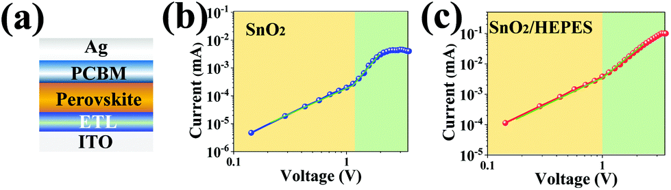
Fig. 1a shows the molecular structure model of HEPES, which contains a hydroxyl (–OH), two nitrogen atoms (N) and a sulfonic group (–HSO3). The abundant functional groups make HEPES a candidate material for SnO2 surface passivation. On the one hand, –OH can react with the surface groups (such as carboxyl) of SnO2, thus blocking the polar groups of SnO2. Fig. S1 (ESI†) shows the Fourier-transform infrared (FTIR) spectrum of fresh SnO2 film after plasma treatment, and it can be seen from the FTIR results that there are absorption peaks in the range of 1580–1644 cm−1 and at 1731 cm−1, which belong to the absorption peaks of the carboxyl group.23 On the other hand, the –HSO3 and N atoms form Lewis adducts with negative/positive charge trap states, which passivate the defects on the surface of the perovskite. Density functional theory (DFT) was used to determine the surface electrostatic potential of HEPES. As shown in Fig. 1b, the –HSO3 and –OH groups are located in the negative and positive electrostatic potential regions, respectively, and these can participate in the coordination or bonding of uncoordinated Pb2+ or halogen defects in the perovskite. It can be seen from the electrostatic potential distribution diagram of the HEPES molecule that –HSO3 is located in the blue region, that is, it belongs to the electron-deficient group. Electron-deficient groups are easy to interact with electron-rich groups. From the DFT calculation, it was further determined that the most easily formed defect in perovskite is the lead iodine substitutions defect (PbI), and its formation energy is 0.43 eV. The formation energies of the Pb vacancy defects and I vacancy defects are 7.27 and 36.24 eV, respectively. PbI defects could easily form and contains many electrons, which act as a lewis acid to coordinate with the existed –HSO3. The interaction between PbI and –HSO3 is benificial to promote the formation of large grains with small defects.24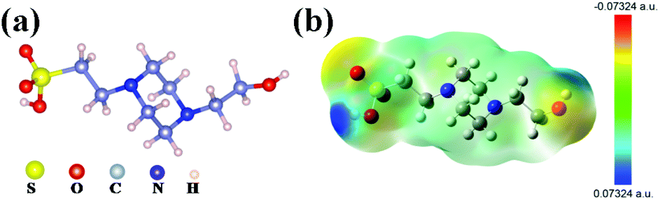 | ||
| Fig. 1 (a) Molecular model of HEPES. (b) Electrostatic potential profile of HEPES. | ||
The FTIR spectroscopy was performed to determine the binding between SnO2 and HEPES. As shown in Fig. S2 (ESI†), the FTIR spectra for HEPES have a strong peak at 3386 cm−1, which is the characteristic peak of the O–H bond. In Fig. 2a, the peak at 1672 cm−1 is assigned to the stretching vibration of the C![[double bond, length as m-dash]](https://www.rsc.org/images/entities/char_e001.gif) O bond. When the SnO2 combines with HEPES, the peak value of CO shifts to a lower wavenumber of 1664 cm−1, which indicates that the SnO2 mainly interacts with the –OH on HEPES. This confirmed that HEPES was chemically anchored on the SnO2 surface. In order to further understand the difference of the optical properties between the ETL films before and after passivation, the optical transmission spectra of the two films were measured, as shown in Fig. 2b. According to reports in the literature, SnO2 nanocrystalline thin films prepared at low temperature have good transmittance due to their excellent anti-reflection ability.25 Interestingly, in the visible region (400–800 nm), both SnO2 and SnO2/HEPES films show good light transmittance. Because the HEPES passivation layer is very thin, the light transmittance of the film does not decrease after the introduction of HEPES, which is conducive to photons reaching the perovskite layer. The water contact angles of SnO2 and SnO2/HEPES films were determined. The results of this are shown in Fig. 2c and d, and the contact angle of the SnO2 film is 14.6° (the average contact angle is 13.56°, see Fig. S3, ESI†). Whereas, the contact angle of the SnO2 substrate coated by HEPES is 11.9° (average is 10.68°), and the hydrophilicity is stronger. Because HEPES has good hydrophilicity, the interface modification with HEPES can cause the perovskite precursor and ETL substrate to infiltrate well, which is beneficial for reducing the Gibbs free energy of the perovskite crystallization and improving the quality of perovskite crystallization.14,26
O bond. When the SnO2 combines with HEPES, the peak value of CO shifts to a lower wavenumber of 1664 cm−1, which indicates that the SnO2 mainly interacts with the –OH on HEPES. This confirmed that HEPES was chemically anchored on the SnO2 surface. In order to further understand the difference of the optical properties between the ETL films before and after passivation, the optical transmission spectra of the two films were measured, as shown in Fig. 2b. According to reports in the literature, SnO2 nanocrystalline thin films prepared at low temperature have good transmittance due to their excellent anti-reflection ability.25 Interestingly, in the visible region (400–800 nm), both SnO2 and SnO2/HEPES films show good light transmittance. Because the HEPES passivation layer is very thin, the light transmittance of the film does not decrease after the introduction of HEPES, which is conducive to photons reaching the perovskite layer. The water contact angles of SnO2 and SnO2/HEPES films were determined. The results of this are shown in Fig. 2c and d, and the contact angle of the SnO2 film is 14.6° (the average contact angle is 13.56°, see Fig. S3, ESI†). Whereas, the contact angle of the SnO2 substrate coated by HEPES is 11.9° (average is 10.68°), and the hydrophilicity is stronger. Because HEPES has good hydrophilicity, the interface modification with HEPES can cause the perovskite precursor and ETL substrate to infiltrate well, which is beneficial for reducing the Gibbs free energy of the perovskite crystallization and improving the quality of perovskite crystallization.14,26
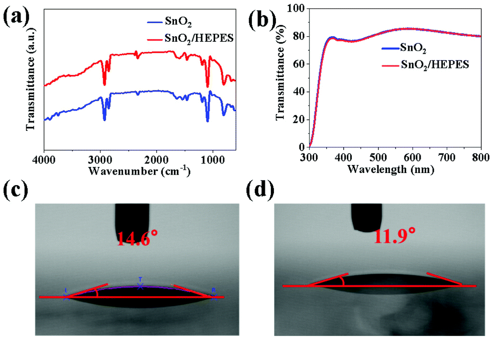 | ||
| Fig. 2 (a) Fourier transform infrared spectra, (b) UV-Vis transmittance spectra of SnO2 and SnO2/HEPES films. Water contact angles of SnO2 (c) and SnO2/HEPES (d) substrates. | ||
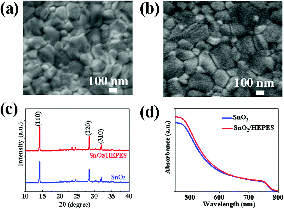
Scanning electron microscopy (SEM) and atomic force microscopy (AFM) were used to further characterize the surface morphology of the substrate before and after passivation. The results are shown in Fig. 3. The SEM images show that the SnO2 nanocrystals are densely arranged and completely covered the ITO surface (Fig. 3a). Due to the thin passivation layer of HEPES, there is almost no obvious effect on the morphology of the substrate after covering the SnO2 surface (Fig. 3b). The 2D and 3D AFM images (Fig. 3c–f) show that the surface roughness of the SnO2/HEPES film is 1.23 nm, which is lower than the 1.57 nm on a bare SnO2 substrate. This result shows that HEPES is beneficial to the growth of the perovskite crystal.27
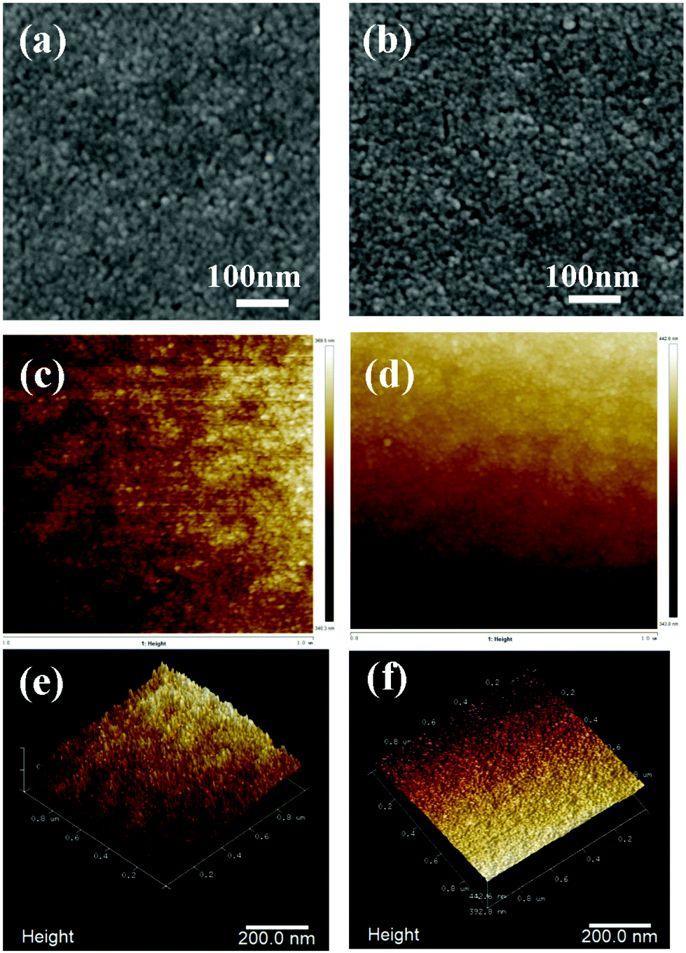 | ||
| Fig. 3 Top-view scanning electron microscopy images of SnO2 layers without (a), and with (b) HEPES. Atomic force microscopy images of SnO2 without (c and e), and with (d and f) HEPES. | ||
The perovskite thin films were prepared on SnO2 and SnO2/HEPES ETL using a one-step anti-solvent method. The morphology of the perovskite films was studied by FE-SEM. In Fig. 4a and b, the perovskite crystal on the SnO2/HEPES substrate is more uniform and denser than that on the SnO2 substrate, and the grain size is also increased. The statistical results of the grain size are shown in Fig. S4 (ESI†). The average size of perovskite crystal on SnO2/HEPES substrate reached 310 nm, which is higher than the 190 nm on the control. The effect of the substrate on the crystal structure of perovskite was determined by X-ray diffraction (XRD). As shown in Fig. 4c, the XRD patterns of perovskite films on SnO2 and SnO2/HEPES substrates show peaks of 14.1° (110), 28.4° (220) and 31.9° (310), which can be indexed as a methylammonium lead triiodide (MAPbI3)tetragonal crystal structure.28,29 Compared with the crystal deposited on the SnO2 substrate, the crystal grown on the SnO2/HEPES substrate has a higher crystal strength and a smaller full width at half maximum (FWHM) (Fig. S5, ESI†), which indicates that the crystallinity of MAPbI3 on SnO2/HEPES is better. The UV-Vis absorption spectrum of the perovskite film is shown in Fig. 4d. The results show that the perovskite films with an SnO2/HEPES underlayer have a higher absorption in the visible range, which is mainly due to the better crystallinity and smoother surface.30 Subsequently, the electron-only devices with a structure of ITO/ETL/perovskite/PCBM/Ag (Fig. 5a) was adopted for space-charge-limited current (SCLC) measurements to test the defect density of the MAPbI3 films deposited on different ETL substrates.31 The J–V curves tested in the dark state are shown in Fig. 5b and c, which includes the ohmic region (linear current–voltage response) at a low bias voltage range and a trap-filling limited region as the current increased significantly. Eqn (1) is used to calculate the trap density (Nt):32,33
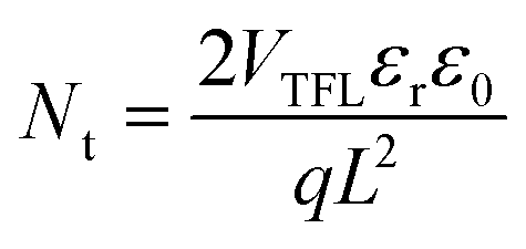 | (1) |
 | ||
| Fig. 4 The SEM images of the perovskite film deposited on SnO2 (a), and on SnO2/HEPES (b) substrate. (c) The XRD, and (d) UV-Vis patterns for perovskite films on different substrates. | ||
 | ||
| Fig. 5 (a) A schematic diagram of electron-only devices with a structure of ITO/ETL/perovskite/PCBM/Ag. (b) and (c) Space-charge-limited current versus voltage of SnO2 and SnO2/HEPES based devices, respectively. | ||
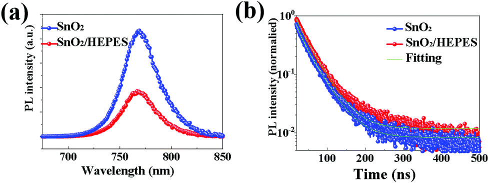
Steady state photoluminescence (PL) and time-resolved photoluminescence (TRPL) were measured to investigate the effect of the HEPES interface layer on the charge extraction and electron transport behavior. As shown in Fig. 6a, the PL intensity of the perovskite film grown on SnO2/HEPES substrate is significantly weaker than that grown on bare SnO2, which indicated that MAPbI3 film grown on SnO2/HEPES substrate exhibits more effective PL quenching than that on the SnO2 substrate. The rapid quenching of the PL indicates that the interface layer of HEPES makes the carrier transport between perovskite and ETL more efficient. Fig. 6b shows the TRPL spectra of perovskite films on SnO2 and SnO2/HEPES substrates. The bi-exponential function eqn (2) is used to fit the PL decay curves.34,35 The fitting parameters are summarized in Table S1 (ESI†).
 | (2) |
 | ||
| Fig. 6 Photoluminescence spectra (a), and time-resolved photoluminescence curves (b) of perovskite film based on different ETLs. | ||
Perovskite solar cells with the structure ITO/ETL/MAPbI3/Spiro-OMeTDA/Ag were prepared using SnO2 and SnO2/HEPES as electron transport layers. The device structure and energy level arrangement of each functional layer as shown in Fig. 7a and b. The SEM image of the cross section of the cell is shown in Fig. 7c, the thickness of the perovskite active layer is about 550 nm. The photovoltaic performance of the cells was measured under one standard simulated sunlight (AM1.5, 100 mW cm−2). Fig. 7d shows the J–V curves of the control and HEPES modified cells. The detailed parameters are listed in Table S2 (ESI†). The PCE of the control reached 18.43% with an open circuit voltage (VOC) of 1.06 V, a short circuit current density (JSC) of 22.57 mA cm−2, and a fill factor (FF) of 76.69%. While JSC and PCE increased to 23.59 mA cm−2 and 20.22%, respectively, for HEPES modified best device. Fig. 7e shows the incident-photon-to-current-efficiency (IPCE) curve of monochromatic light incidence. The integrated current of the HEPES modified cells increased from 21.69 to 23.01 mA cm−2. This shows the superiority of the charge injection and collection of the HEPES modified devices. In order to further study the effect of the HEPES interface layer on the performance of the solar cell, the J–V curves of the cell in the dark were measured. As shown in Fig. S6 (ESI†), the dark current density of the HEPES modified device is lower than that of the control device, which indicates that the current leakage phenomenon is effectively suppressed after the interface modification. This is consistent with the measurement results of the steady-state PL and TRPL. It further shows that the surface modification layer of HEPES obviously reduced the charge recombination. Next the electrochemical impedance spectroscopy (EIS) of the operational SnO2 and SnO2/HEPES based perovskite solar cells were measured under dark conditions and the Nyquist plots (bias = 0.8 V) are shown in Fig. 7f. For the two devices, we applied an equivalent circuit model to fit the series resistance (Rs) and recombination resistance (Rrec) and the fitting parameters are summarized in Table S3 (ESI†), and the equivalent circuit model is shown in the inset of Fig. 7f. Based on the fitting results, the Rs was found to decrease from 43 Ω (for the SnO2-based device) to 32 Ω (for the SnO2/HEPES device), which is consistent with the improved electron extraction at the cathode interface. The Rrec increases from 733 Ω (for the SnO2-based device) to 1053 Ω (for the SnO2/HEPES device), indicating the effectively suppressed carrier recombination in the perovskite solar cells with the inserted HEPES layer.
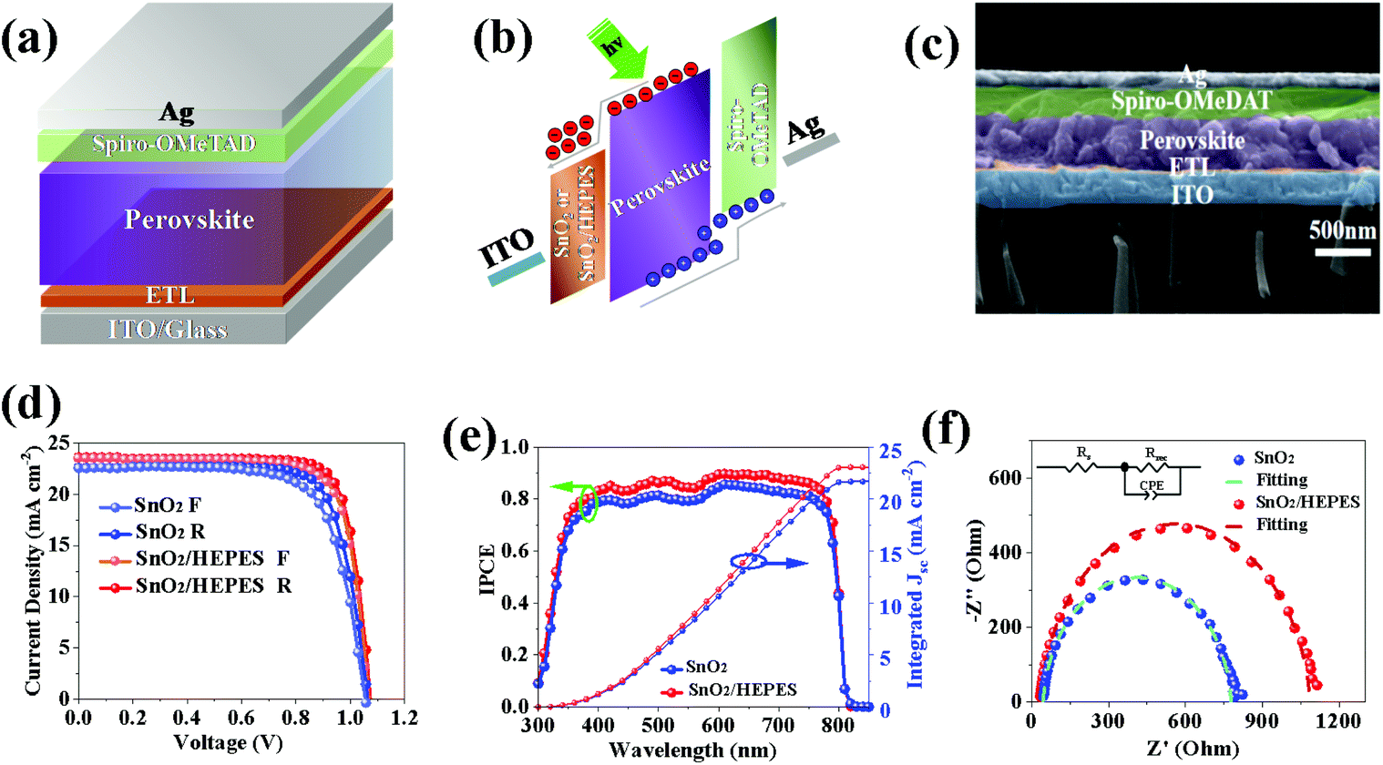 | ||
| Fig. 7 (a) Device structure of the p-i-n PSCs, (b) corresponding energy-level diagram of the structure shown in (a), (c) cross-sectional SEM image of the device, (d) the J–V curves of the best PSCs under reverse and forward scans, (e) the IPCE spectra, and integrated Jsc of the corresponding devices, and (f) the Nyquist plot of the impedance spectroscopy of SnO2 and SnO2/HEPES based perovskite solar cells measured in the dark at 0.6 V, together with the fitting results with an equivalent circuit model (inset). | ||
Long-term stability is another key indicator to evaluate the performance of the perovskite solar cells. The long-term stability of perovskite solar cells stored under ambient conditions without encapsulation is tested further. As shown in Fig. S7 (ESI†), for the normalized PCE decay versus storage time, 86% of the initial PCE is maintained for the SnO2/HEPES based sample after 30 d of storage in an ambient environment (T ≈25 °C, RH ≈50%), whereas the control device only retains 74% of the initial efficiency after one month. Considering the improvement of film quality, in particular for the compact perovskite with large grains for the SnO2/HEPES sample, the probability of water molecules diffusing into the internal region of the perovskite film will be reduced. Therefore, under the same environment (T ≈25 °C, RH ≈50%), the decomposition of perovskite deposited on SnO2/HEPES is minimized, and finally the stability of the device is improved.
The transient photocurrent (TPC) decay and transient photovoltage (TPV) decay are important means to study the charge transfer performance of the solar cell devices. As Fig. 8a shows, compared to the SnO2-based sample, the SnO2/HEPES based device gave a reduced TPC response, showing that charge extraction and transmission is more effective than that in the control device. In Fig. 8b, the TPV response of the SnO2/HEPES sample exhibits a longer lifetime than that of the control solar cell, which proves that carrier recombination is effectively suppressed in the SnO2/HEPES based device.37 The charge transport characteristics show that HEPES effectively passivates the ETL/perovskite interface, promotes the formation of high-quality perovskite, reduces the perovskite defect density, and promotes the carrier transport of the device, which enhances the PCE of the PSCs.
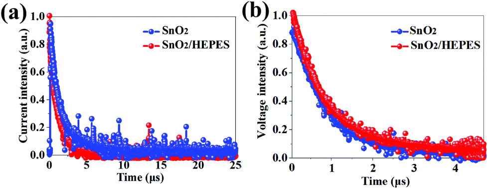 | ||
| Fig. 8 Normalized transient photocurrent (a), and transient optical-voltage (b) for PSCs without and with a HEPES layer. | ||
Conclusions
In conclusion, HEPES is used to passivate the surface of the SnO2 film. The results show that high quality perovskite thin films with improved crystallinity are obtained on the SnO2/HEPES substrates. In addition, HEPES can passivate SnO2 surface defects and improve the efficiency of the electron transport. The results showed that the PCE of HEPES modified PSCs was up to 20.22%. The improvement of device performance is mainly due to the introduction of the HEPES interface layer to adjust the interface energy level, improve the crystallinity of the perovskite film and reduce the interface defects. The EIS and TPV/TPC results further indicate that the HEPES modified PSCs have a lower carrier transfer resistance, lower leakage current density, and lower interface charge accumulation.Conflicts of interest
There are no conflicts to declare.Acknowledgements
This work was supported by the Natural Science Foundation of Henan Province (No. 202300410073) and the China Postdoctoral Science Foundation (2021M690907).Notes and references
- A. Kojima, K. Teshima, Y. Shirai and T. Miyasaka, Organometal halide perovskites as visible-light sensitizers for photovoltaic cells, J. Am. Chem. Soc., 2009, 131, 6050–6051 CrossRef CAS PubMed.
- J. Jeong, M. Kim, J. Seo, H. Z. Lu, P. Ahlawat, A. Mishra, Y. G. Yang, M. A. Hope, F. T. Eickemeyer, M. Kim, Y. J. Yoon, I. W. Choi, B. P. Darwich, S. J. Choi, Y. Jo, J. H. Lee, B. Walker, S. M. Zakeeruddin, L. Emsley, U. Rothlisberger, A. Hagfeldt, D. S. Kim, M. Grätzel and J. Y. Kim, Pseudo-halide anion engineering for α-FAPbI3 perovskite solar cells, Nature, 2021, 59, 2381 Search PubMed.
- E. T. Hoke, D. J. Slotcavage, E. R. Dohner, A. R. Bowring, H. I. Karunadasa and M. McGehee, Reversible photo-induced trap formation in mixed-halide hybrid perovskites for photovoltaics, Chem. Sci., 2015, 6, 613–617 RSC.
- S.-H. Jeong, J. Park, T.-H. Han, F. Zhang, K. Zhu, J. S. Kim, M.-H. Park, M. O. Reese, S. Yoo and T.-W. Lee, Characterizing the efficiency of perovskite solar cells and light-emitting diodes, Joule, 2020, 4, 1206–1235 CrossRef CAS.
- T. Matsushima, S. Hwang, A. S. Sandanayaka, C. Qin, S. Terakawa, T. Fujihara, M. Yahiro and C. Adachi, Solution–processed organic-inorganic perovskite field-effect transistors with high hole mobilities, Adv. Mater., 2016, 28, 10275–10281 CrossRef CAS PubMed.
- Q. Dong, Y. Fang, Y. Shao, P. Mulligan, J. Qiu, L. Cao and J. Huang, Electron-hole diffusion lengths >175 μm in solution-grown CH3NH3PbI3 single crystals, Science, 2015, 347, 967–970 CrossRef CAS PubMed.
- A. Perulli, A. Balena, M. Fernandez, G. Nedelcu, A. Cretí, M. V. Kovalenko, M. Lomascolo and M. Anni, Full-color tuning in binary polymer: perovskite nanocrystals organic-inorganic hybrid blends, Appl. Phys. Lett., 2018, 112, 171904 CrossRef.
- N. Zibouche and M. Islam, Structure-electronic property relationships of 2D ruddlesden-popper tin-and lead-based iodide perovskites, ACS Appl. Mater. Interfaces, 2020, 12, 15328–15337 CrossRef CAS PubMed.
- J. Wang, K. Datta, C. H. Weijtens, M. M. Wienk and R. A. Janssen, Insights into fullerene passivation of SnO2 electron transport layers in perovskite solar cells, Adv. Funct. Mater., 2019, 29, 1905883 CrossRef CAS.
- Y. Lee, S. Lee, G. Seo, S. Paek, K. T. Cho, A. J. Huckaba, M. Calizzi, D. W. Choi, J. S. Park and D. J. Lee, Efficient planar perovskite solar cells using passivated tin oxide as an electron transport layer, Adv. Sci., 2018, 5, 1800130 CrossRef PubMed.
- Q. Jiang, X. Zhang and J. You, SnO2: a wonderful electron transport layer for perovskite solar cells, Small, 2018, 14, 1801154 CrossRef PubMed.
- Y. Ai, W. Liu, C. Shou, J. Yan, N. Li, Z. Yang, W. Song, B. Yan, J. Sheng and J. Ye, SnO2 surface defects tuned by (NH4)2S for high-efficiency perovskite solar cells, Sol. Energy, 2019, 194, 541–547 CrossRef CAS.
- S. Zhang, H. Si, W. Fan, M. Shi, M. Li, C. Xu, Z. Zhang, Q. Liao, A. Sattar and Z. J. Kang, Graphdiyne: bridging SnO2 and perovskite in planar solar cells, Angew. Chem., Int. Ed., 2020, 59, 11573–11582 CrossRef CAS PubMed.
- D. Yang, R. Yang, K. Wang, C. Wu, X. Zhu, J. Feng, X. Ren, G. Fang, S. Priya and S. F. Liu, High efficiency planar-type perovskite solar cells with negligible hysteresis using EDTA-complexed SnO2, Nat. Commun., 2018, 9, 1–11 CrossRef.
- Q. Liu, X. Zhang, C. Li, H. Lu, Z. Weng, Y. Pan, W. Chen, X.-C. Hang, Z. Sun and Y. J. Zhan, Effect of tantalum doping on SnO2 electron transport layer via low temperature process for perovskite solar cells, Appl. Phys. Lett., 2019, 115, 143903 CrossRef.
- X. Ren, D. Yang, Z. Yang, J. Feng, X. Zhu, J. Niu, Y. Liu, W. Zhao and S. F. Liu, Solution-processed Nb: SnO2 electron transport layer for efficient planar perovskite solar cells, ACS Appl. Mater. Interfaces, 2017, 9, 2421–2429 CrossRef CAS PubMed.
- J. Ma, G. Yang, M. Qin, X. Zheng, H. Lei, C. Chen, Z. Chen, Y. Guo, X. Zhao and G. J. Fang, MgO nanoparticle modified anode for highly efficient SnO2-based planar perovskite solar cells, Adv. Sci., 2017, 4, 1700031–1700031 CrossRef.
- Z. Zhu, Y. Bai, X. Liu, C. Chueh, S. Yang and A. K. Jen, Enhanced efficiency and stability of inverted perovskite solar cells using highly crystalline SnO2 nanocrystals as the robust electron–transporting layer, Adv. Mater., 2016, 28, 6478–6484 CrossRef CAS PubMed.
- P. Zhu, S. Gu, X. Luo, Y. Gao, S. Li, J. Zhu and H. Tan, Simultaneous contact and grain–boundary passivation in planar perovskite solar cells using SnO2−KCl composite electron transport layer, Adv. Energy Mater., 2020, 10, 1903083 CrossRef CAS.
- C. Li, H. Li, Z. N. Zhu, N. Y. Cui, Z. A. Tan and R. S. Yang, Perovskite passivation strategies for efficient and stable solar cells, Sol. RRL, 2021, 5, 2000579 CrossRef CAS.
- K. Liu, S. Chen, J. Wu, H. Zhang, M. Qin, X. Lu, Y. Tu, Q. Meng and X. J. E. Zhan, Fullerene derivative anchored SnO2 for high-performance perovskite solar cells, Energy Environ. Sci., 2018, 11, 3463–3471 RSC.
- Y. Dong, W. Li, X. Zhang, Q. Xu, Q. Liu, C. Li and Z. Bo, Highly efficient planar perovskite solar cells via interfacial modification with fullerene derivatives, Small, 2016, 12, 1098–1104 CrossRef CAS.
- P.L. Qin, T. Wu, Z. C. Wang, X. L. Zheng, X. L. Yu, G. J. Fang and G. Li, Vitrification transformation of poly(ethylene oxide) activating interface passivation for high-efficiency perovskite solar cells, Sol. RRL, 2019, 3, 1900134 CrossRef CAS.
- W. J. Yin, T. Shi and Y. Yan, Unusual defect physics in CH3NH3PbI3 perovskite solar cell absorber, Appl. Phys. Lett., 2014, 104, 063903 CrossRef.
- W. Ke, G. Fang, Q. Liu, L. Xiong, P. Qin, H. Tao, J. Wang, H. Lei, B. Li and J. Wan, Low-temperature solution-processed tin oxide as an alternative electron transporting layer for efficient perovskite solar cells, J. Am. Chem. Soc., 2015, 137, 6730–6733 CrossRef CAS.
- P. Zhang, F. Yang, M. A. Kamarudin, C. H. Ng, G. Kapil, T. Ma and S. Hayase, Performance enhancement of mesoporous TiO2-based perovskite solar cells by SbI3 interfacial modification layer, ACS Appl. Mater. Interfaces, 2018, 10, 29630–29637 CrossRef CAS PubMed.
- M. Zhang, F. Wu, D. Chi, K. Shi and S. Huang, High-efficiency perovskite solar cells with poly (vinylpyrrolidone)-doped SnO2 as an electron transport layer, Mater. Adv., 2020, 1, 617–624 RSC.
- Q. Guo, F. L. Yuan, B. Zhang, S. J. Zhou, J. Zhang, Y. M. Bai, L. Z. Fan, T. Hayat, A. Alsaedi and Z. A. Tan, Passivation of the grain boundaries of CH3NH3PbI3 using carbon quantum dots for highly efficient perovskite solar cells with excellent environmental stability, Nanoscale, 2019, 11, 115–124 RSC.
- D. Yang, R. Yang, X. Ren, X. Zhu, Z. Yang, C. Li and S. Liu, Hysteresis-suppressed high-efficiency flexible perovskite solar cells using solid-state ionic-liquids for effective electron transport, Adv. Mater., 2016, 28, 5206–5213 CrossRef CAS PubMed.
- F. Yang, P. Zhang, M. A. Kamarudin, G. Kapil, T. Ma and S. Hayase, Addition effect of pyreneammonium iodide to methylammonium lead halide perovskite-2D/3D heterostructured perovskite with enhanced stability, Adv. Funct. Mater., 2018, 28, 1804856 CrossRef.
- H. Su, J. Zhang, Y. Hu, X. Du, Y. Yang, J. You, L. Gao and S. Liu, Fluoroethylamine Engineering for effective passivation to attain 23.4% efficiency perovskite solar cells with superior stability, Adv. Energy Mater., 2021, 23, 2101454 CrossRef.
- H. Jiang, X. Qu, L. He, Z. Lv, D. Li, F. Wang, L. Fan, J. Yang, L. Yang and Y. Yan, A design strategy of additive molecule for PSCs: anchoring intrinsic properties of functional groups by suppressing long-range conjugation effect, J. Energy Chem., 2021, 131676 Search PubMed.
- S. Yang, Q. Han, L. Wang, Y. Zhou, F. Yu, C. Li, X. Cai, L. Gao, C. Zhang and T. Ma, Over 23% Power Conversion Efficiency of Planar Perovskite Solar Cells via Bulk Heterojunction Design, Chem. Eng. J., 2021, 131838 CrossRef CAS.
- X. Li, W. Li, Y. Yang, X. Lai, Q. Su, D. Wu, G. Li, K. Wang, S. Chen and X. W. Sun, Defects passivation with dithienobenzodithiophene–based π–conjugated polymer for enhanced performance of perovskite solar cells, Sol. RRL, 2019, 3, 1900029 CrossRef.
- Z. Zhu, Y. Bai, H. K. H. Lee, C. Mu, T. Zhang, L. Zhang, J. Wang, H. Yan, S. K. So and S. Yang, Polyfluorene derivatives are high–performance organic hole-transporting materials for inorganic-organic hybrid perovskite solar cells, Adv. Funct. Mater., 2014, 24, 7357–7365 CrossRef CAS.
- Y. Yang, J. Wu, X. Wang, Q. Guo, X. Liu, W. Sun, Y. Wei, Y. Huang, Z. Lan and M. Huang, Suppressing vacancy defects and grain boundaries via ostwald ripening for high–performance and stable perovskite solar cells, Adv. Mater., 2020, 32, 1904347 CrossRef CAS.
- W. Chen, Y. Wu, Y. Yue, J. Liu, W. Zhang, X. Yang, H. Chen, E. Bi, I. Ashraful and M. Grätzel, Efficient and stable large-area perovskite solar cells with inorganic charge extraction layers, Science, 2015, 350, 944–948 CrossRef CAS.
Footnote |
| † Electronic supplementary information (ESI) available. See DOI: 10.1039/d1nr05939d |
| This journal is © The Royal Society of Chemistry 2022 |