
 Open Access Article
 This Open Access Article is licensed under a
 Creative Commons Attribution 3.0 Unported Licence
Size selection and thin-film assembly of MoS2 elucidates thousandfold conductivity enhancement in few-layer nanosheet networks†
Sean P.
Ogilvie
 *a,
Matthew J.
Large
a,
Hannah J.
Wood
a,
Aline
Amorim Graf
a,
Frank
Lee
a,
Jonathan P.
Salvage
b,
Alice A. K.
King
a and
Alan B.
Dalton
*a
*a,
Matthew J.
Large
a,
Hannah J.
Wood
a,
Aline
Amorim Graf
a,
Frank
Lee
a,
Jonathan P.
Salvage
b,
Alice A. K.
King
a and
Alan B.
Dalton
*a
aUniversity of Sussex, Brighton, BN1 9RH, UK. E-mail: s.ogilvie@sussex.ac.uk; a.b.dalton@sussex.ac.uk
bUniversity of Brighton, Brighton, BN2 4GJ, UK
First published on 17th December 2021
Abstract
Printed electronics based on liquid-exfoliated nanosheet networks are limited by inter-nanosheet junctions and thick films which hinder field-effect gating. Here, few-layer molybdenum disulfide nanosheets are assembled by Langmuir deposition into thin films, and size selection is shown to lead to a thousandfold conductivity enhancement with potential applicability to all nanosheet networks.
Printed electronic devices such as thin-film transistors require solution-processable materials which are sufficiently thin to allow field-effect gating while retaining measurable device resistances. Liquid-exfoliated two-dimensional (2D) nanosheet networks have shown much promise for printed electronics1–3 but significant challenges remain for the development of practical devices based on networks of semiconducting nanosheet such as molybdenum disulfide (MoS2). Firstly, network mobility and thereby conductivity are limited by inter-nanosheet junctions. Furthermore, random networks exhibit further-reduced conductivity below a critical thickness,4 meaning that thicker films are required to achieve measurable device resistances. Low mobilities and thick films have hampered efforts to realise field-effect gating of semiconducting nanosheet networks, with electrolyte gating required for practical devices.2,5,6 By contrast, electrochemical exfoliation of MoS2 has been demonstrated to yield large few-layer nanosheets with improved junctions for high-performance field-effect transistors,7 albeit with a compromise between performance, scalability and printability.8 In addition, this approach has enabled devices to be prepared from thin films assembled at liquid–liquid interfaces.9 It would therefore be desirable to realise such performance enhancements with scalable printable liquid-exfoliated nanosheets. To this end, this study explores size selection of liquid-exfoliated MoS2 to assemble networks of few-layer nanosheets and utilises Langmuir deposition as a route to achieve thin dense-packed networks with potential for device applications.
Langmuir deposition is a film formation technique capable of assembling monolayers of particulates at the air–water interface. While this technique has been applied to a range of 2D nanosheets,10–16 its potential for pristine semiconducting thin films remains unexplored. This is likely because of the challenge of identifying appropriate solvents for exfoliation and deposition. As illustrated in Fig. 1a, the need for low boiling point precludes prototypical exfoliating solvent N-methyl-2-pyrrolidone (NMP), while the need for surface energy and Hansen parameter matching for exfoliation precludes common Langmuir solvents such as chloroform. Based on these requirements and previous work on solvent spreading at the air–water interface,17 we have identified cyclopentanone (CPO) as an ideal solvent for exfoliation and Langmuir deposition of MoS2. In practice, exfoliation in CPO by ultrasonication and size selection by centrifugation yields few-layer nanosheet dispersions with high concentration to facilitate Langmuir deposition.
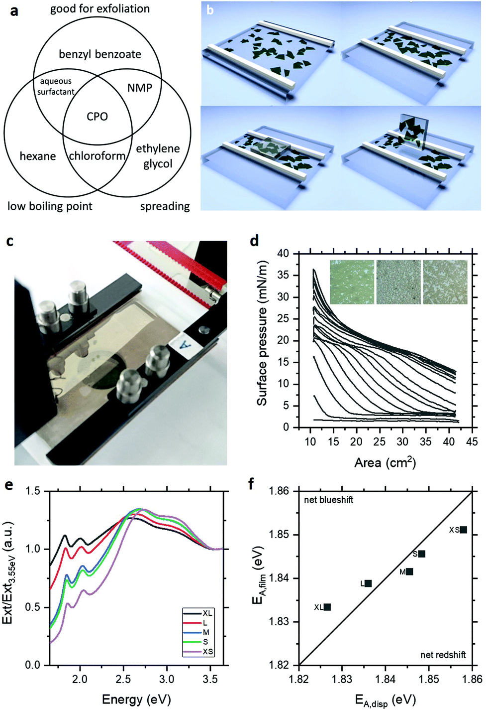 | ||
| Fig. 1 (a) Venn diagram illustrating solvent selection criteria for Langmuir deposition. (b) Schematic illustrating Langmuir deposition of nanosheet networks. (c) Photograph of dense-packed MoS2 film on water subphase. (d) Surface pressure-area isotherms for increasing volumes of deposited material and inset micrographs showing film compression. (e) Extinction spectra of size-selected MoS2 in CPO dispersions showing A-exciton redshift with increasing layer number to energies below those in established metrics due to solvatochromism. (f) Comparison of A-exciton energy in dispersion and film showing net blueshift for some largest nanosheets on reduction on solvatochromic effects after deposition. | ||
As illustrated schematically in Fig. 1b, these nanosheets can be assembled at the air–water interface to form floating films which can be compressed into dense-packed networks and deposited by horizontal Langmuir–Schaefer (L–S) deposition. Fig. 1c shows a typical Langmuir film of MoS2 with the green colouration highlighting the few-layer nature of the assembled nanosheets and the appreciable optical absorbance indicating that the films are formed of more than a single nanosheet's thickness. This latter point is consistent with observation of islands of nanosheets forming during assembly, which is well-understood for hydrophobic materials.16 This film formation is also evident in the surface pressure-area isotherms shown in Fig. 1d acquired during Langmuir assembly with sequential deposition and cycling of MoS2, where surface pressure increases in response to the connectivity of the islands, shown in the inset micrographs. These films can be deposited onto sputtered gold electrodes on glass or, preferably, polyethylene terephthalate (PET) by horizontal L–S transfer to yield semi-transparent (T ∼ 40%) coatings over large areas, indicating an area-averaged thickness of <10 monolayers given the ∼85% monolayer absorbance of MoS2.18 This semitransparency enables UV-visible extinction spectroscopy to be performed in transmission for direct comparison to their starting dispersions. To examine these changes as a function of MoS2 nanosheet thickness, liquid cascade centrifugation19 was used to prepare size-selected samples with a range of average layer numbers and lateral sizes.20 The extinction spectra for Langmuir films deposited from these dispersions are shown in Fig. 1e, with the spectra for the dispersions in the ESI Fig. S3.† Both the films and dispersion spectra show the expected blueshift of the A-exciton peak with decreasing layer number. Interestingly, the dispersions exhibit systematic peak shifts at longer wavelengths than those observed previously21 and, as a result, the films of the largest nanosheets exhibit a net blueshift relative to the starting dispersion as shown in Fig. 1f. Since this would suggest unphysical reduction of layer number on deposition and nanosheets do not restack with the atomic registry required to modulate optical properties,22 these effects are attributed to solvatochromism of the excitonic peaks in the CPO dispersions which are eliminated to vary degrees in the deposited films. Indeed, ketone solvents are known to result in solvatochromic red shifts in the photoluminescence of single-flake MoS2 of up to 16 meV.23 This corresponds to a factor of two increase in layer number using the established spectroscopic metrics and highlights the potential of solvatochromic effects to influence measurements of nanosheet properties (see ESI†).
Having demonstrated that few-layer nanosheets can be assembled into dense-packed thin films, atomic force microscopy (AFM) was employed for direct measurement of morphology and film thickness. Fig. 2a shows an AFM height image of a representative film edge with nanosheets forming a uniform film over tens of microns, despite local disorder typical of nanosheet networks. Fig. 2b shows an AFM height image of a representative dense-packed region of the film where individual and overlapping nanosheets and the substrate can be resolved. Importantly, the film thickness is in the range 20–50 nm, as shown by the line sections in Fig. 2c and d. This indicates that Langmuir deposition can indeed assemble dense-packed films of few-layer nanosheets with thicknesses which may be compatible with field-effect gating. Scanning electron microscopy (SEM), shown in Fig. 2e, indicates the film uniformity over large length scales and suggests appreciable network conductivity.
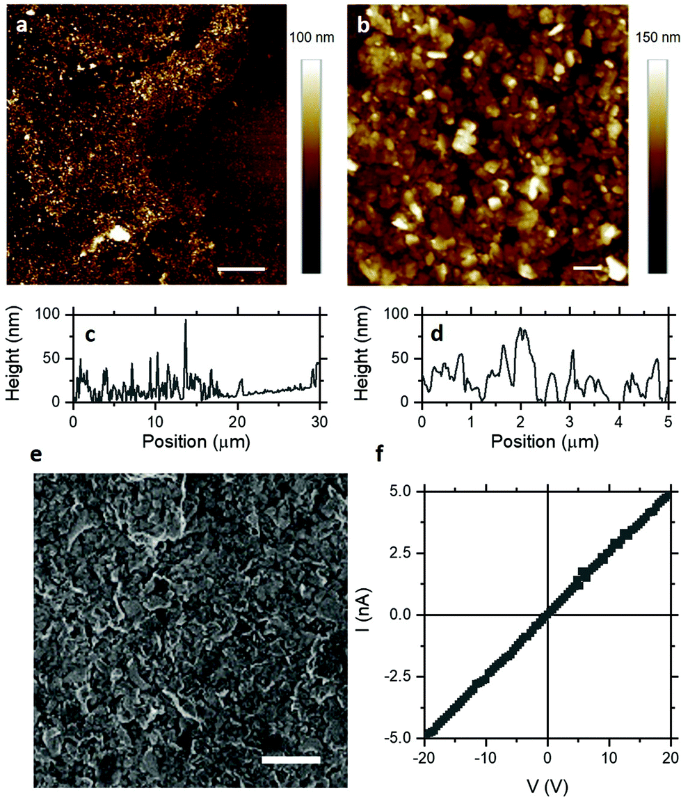 | ||
| Fig. 2 (a) AFM image, scale bar 5 μm, showing edge of film with dense-packed nanosheets, shown in (b), scale bar 500 nm and thin film formation with line sections in (c) and (d). (e) SEM image indicating film uniformity and non-negligible conductivity, scale bar 1 μm (f) Representative I–V characteristic for MoS2 thin films showing ∼GΩ sq−1 sheet resistance in thin films of single centrifugation nanosheets, indicating network conductivity of ∼10−3 S m−1. | ||
Electrical properties of MoS2 Langmuir films can be studied by measuring I–V characteristics such as that shown in Fig. 2e. These I–V characteristics exhibit excellent Ohmic behaviour, with improved linearity even relative to previously-reported MoS2 nanosheet networks with good Ohmic contracts.24,25 This has been attributed to reduction in the Schottky barrier at the MoS2–gold interface for multilayers26,27 and eliminated for monolayers.28–30 The electrical conductivity of liquid-exfoliated MoS2 nanosheet networks has been reported to be in the range 10−6–10−5 S m−1.2,4,25,31,32 At the thicknesses of these Langmuir films, such conductivities would result in sheet resistances >1 TΩ sq−1, which would likely require high aspect ratio channels to achieve measurable device resistance. Fig. 2e shows a representative I–V characteristic for the MoS2 Langmuir films studied here for a square channel (l/w ∼ 1), with sheet resistance of ∼4 GΩ sq−1. Significantly, this yields an electrical conductivity of ∼10−3 S m−1 – two to three orders of magnitude higher than previously reported for MoS2 nanosheet networks. This suggests that some aspect of the particular processing employed improves charge transport in these films, which may enable subsequent applications in electronic devices.
It is therefore important to consider the processing and properties to those of previously-reported MoS2 nanosheet networks. Fig. 3a shows a plot of sheet resistance and thickness to allow comparison of both practical applicability and absolute conductivity, with the latter forming contours in the plot. Nanosheet networks from the literature were prepared by exfoliation in NMP and deposited variously by vacuum filtration,31 thick-film Langmuir-type assembly,25 or inkjet printing,2,4 yielding films with thicknesses between 100 nm and 2 μm and sheet resistances corresponding to conductivity clustered around 10−6 S m−1. By contrast, MoS2 Langmuir films prepared by exfoliation in CPO have thicknesses as low as 20 nm and conductivity as high as 10−3 S m−1. While this discrepancy could be attributed to the different solvent and/or deposition process, additional few-layer dispersions were prepared using the same conditions in NMP and aqueous Triton X-100 and films prepared by vacuum filtration and spray deposition respectively. As shown in Fig. 3a, these samples are consistent with the increased conductivity of the CPO-exfoliated MoS2 Langmuir films, suggesting the enhancement to be the result of a general and transferable modification of MoS2 nanosheets or networks or both.
 | ||
| Fig. 3 (a) Sheet resistance vs film thickness showing thinner films and higher conductivities for Langmuir films and other MoS2 networks in this work compared to literature values. (b) Conductivity vs average nanosheet length showing exponent decay with length, for both size-selected few-layer networks and larger thicker nanosheets reported in literature. | ||
As such, the outstanding difference between the nanosheet networks previously reported (∼10−6 S m−1) and those reported here (∼10−3 S m−1) is the size selection procedure. Previous studies either performed no size selection or preferentially removed smaller thinner nanosheets, variously to prevent negative photoconductivity4,25 or charge traps due to band gap mismatch.2 By contrast, this work has focused on small few-layer nanosheets to allow application of spectroscopic metrics and thin film formation. To investigate the effect of this size selection, a further centrifugation cascade was performed, exfoliating in surfactant solution to maximise yield and allow film formation from all fractions. Electrical conductivity as a function of nanosheet length is shown in Fig. 3b, with network conductivity increasing from 10−6 to 10−3 S m−1 with decreasing nanosheet size, with the literature conductivities also described by this size dependence. This continuous scaling suggests the enhanced conductivity to be an emergent rather than anomalous effect which is predominantly dictated by nanosheet size and thickness.
These emergent effects can potentially be related to the structure and properties as nanosheet size and thickness is reduced. Small nanosheets inherently have an increased fraction of edge sites21 which can comprise vacancies or functional groups. In MoS2 in particular, sulfur vacancies are formed very readily33,34 and contribute a state very close to the conduction band. The effect of this is to pin the Fermi level close the conduction band edge, resulting in n-type conduction in MoS2.35 As such, the increased density of edge vacancies could contribute an increased density of dopant states and increase the carrier density of the network. Additionally, functionalisation at edge sites has the potential to modify properties through formation of oxides to which MoS2 nanosheets are known to be susceptible, with improved hydrogen evolution catalysis with both increasing oxide content36 and decreasing nanosheet size,37 potentially related through an underlying conductivity increase. While MoS2 can be easily oxidised to conductive MoO2, subsequent oxidation to insulating MoO3![[thin space (1/6-em)]](https://www.rsc.org/images/entities/char_2009.gif) 36,38 and the absence of strong oxide peaks in the Raman suggest there is limited influence of edge functionalisation on the overall nanosheet properties. Furthermore, any doping of the nanosheets could only increase the network conductivity by a corresponding factor, suggesting increases in carrier density alone would be insufficient to account for the thousandfold conductivity increase. It is therefore likely that network mobility, understood to be dictated by transport-limiting junctions and network structure, is also significantly increased with decreasing nanosheet size. This is consistent with recent work which has observed increased conductivity for smaller nanosheets of others materials,39,40 suggesting this may be a general phenomenon likely related to modification of network structure and junction resistance for thinner, more flexible nanosheets.
36,38 and the absence of strong oxide peaks in the Raman suggest there is limited influence of edge functionalisation on the overall nanosheet properties. Furthermore, any doping of the nanosheets could only increase the network conductivity by a corresponding factor, suggesting increases in carrier density alone would be insufficient to account for the thousandfold conductivity increase. It is therefore likely that network mobility, understood to be dictated by transport-limiting junctions and network structure, is also significantly increased with decreasing nanosheet size. This is consistent with recent work which has observed increased conductivity for smaller nanosheets of others materials,39,40 suggesting this may be a general phenomenon likely related to modification of network structure and junction resistance for thinner, more flexible nanosheets.
Conclusions
Exfoliation and size selection of MoS2 in CPO yields few-layer nanosheets which facilitate interfacial Langmuir film formation. These thin films exhibit conductivities of ∼10−3 S m−1, a thousandfold enhancement over MoS2 nanosheet networks reported in the literature. By extending to other exfoliating solvents and deposition techniques, this enhancement is attributed to the size selection of few-layer small nanosheets with reduced junction resistance and potentially enhanced network mobility. This highlights the potential of size selection and Langmuir deposition to improve transport properties and reduce film thickness for printed electronic devices.Author contributions
The study was devised by SPO and ABD. Experimental work was performed by SPO, MJL, HJW, AAG, FL, JPS and AAKK. SPO wrote the manuscript with assistance from MJL and ABD.Conflicts of interest
There are no conflicts to declare.References
- T. Carey, S. Cacovich, G. Divitini, J. Ren, A. Mansouri, J. M. Kim, C. Wang, C. Ducati, R. Sordan and F. Torrisi, Nat. Commun., 2017, 8, 1202 CrossRef PubMed.
- A. G. Kelly, T. Hallam, C. Backes, A. Harvey, A. S. Esmaeily, I. Godwin, J. Coelho, V. Nicolosi, J. Lauth, A. Kulkarni, S. Kinge, L. D. A. Siebbeles, G. S. Duesberg and J. N. Coleman, Science, 2017, 356, 69–73 CrossRef CAS PubMed.
- R. Worsley, L. Pimpolari, D. McManus, N. Ge, R. Ionescu, J. A. Wittkopf, A. Alieva, G. Basso, M. Macucci, G. Iannaccone, K. S. Novoselov, H. Holder, G. Fiori and C. Casiraghi, ACS Nano, 2019, 13, 54–60 CrossRef CAS PubMed.
- D. J. Finn, M. Lotya, G. Cunningham, R. J. Smith, D. McCloskey, J. F. Donegan and J. N. Coleman, J. Mater. Chem. C, 2014, 2, 925–932 RSC.
- T. M. Higgins, S. Finn, M. Matthiesen, S. Grieger, K. Synnatschke, M. Brohmann, M. Rother, C. Backes and J. Zaumseil, Adv. Funct. Mater., 2018, 1804387 Search PubMed.
- S. Ippolito, A. G. Kelly, R. Furlan de Oliveira, M.-A. Stoeckel, D. Iglesias, A. Roy, C. Downing, Z. Bian, L. Lombardi, Y. A. Samad, V. Nicolosi, A. C. Ferrari, J. N. Coleman and P. Samorì, Nat. Nanotechnol., 2021, 1–7 Search PubMed.
- Z. Lin, Y. Liu, U. Halim, M. Ding, Y. Liu, Y. Wang, C. Jia, P. Chen, X. Duan, C. Wang, F. Song, M. Li, C. Wan, Y. Huang and X. Duan, Nature, 2018, 562, 254 CrossRef CAS PubMed.
- T. Carey, A. Arbab, L. Anzi, H. Bristow, F. Hui, S. Bohm, G. Wyatt-Moon, A. Flewitt, A. Wadsworth, N. Gasparini, J. M. Kim, M. Lanza, I. McCulloch, R. Sordan and F. Torrisi, Adv. Electron. Mater., 2021, 7, 2100112 CrossRef CAS.
- J. Neilson, M. P. Avery and B. Derby, ACS Appl. Mater. Interfaces, 2020, 12, 25125–25134 CrossRef CAS PubMed.
- L. J. Cote, F. Kim and J. Huang, J. Am. Chem. Soc., 2009, 131, 1043–1049 CrossRef CAS PubMed.
- R. Y. N. Gengler, A. Veligura, A. Enotiadis, E. K. Diamanti, D. Gournis, C. Józsa, B. J. van Wees and P. Rudolf, Small, 2010, 6, 35–39 CrossRef CAS PubMed.
- Q. Zheng, W. H. Ip, X. Lin, N. Yousefi, K. K. Yeung, Z. Li and J.-K. Kim, ACS Nano, 2011, 5, 6039–6051 CrossRef CAS PubMed.
- H. Kim, C. Mattevi, H. J. Kim, A. Mittal, K. A. Mkhoyan, R. E. Riman and M. Chhowalla, Nanoscale, 2013, 5, 12365–12374 RSC.
- A. Fahimi, I. Jurewicz, R. J. Smith, C. S. Sharrock, D. A. Bradley, S. J. Henley, J. N. Coleman and A. B. Dalton, Carbon, 2013, 64, 435–443 CrossRef CAS.
- Y. Zhang, L. Xu, W. R. Walker, C. M. Tittle, C. J. Backhouse and M. A. Pope, J. Mater. Chem. C, 2017, 5, 11275–11287 RSC.
- A. Kalosi, M. Demydenko, M. Bodik, J. Hagara, M. Kotlar, D. Kostiuk, Y. Halahovets, K. Vegso, A. Marin Roldan, G. S. Maurya, M. Angus, P. Veis, M. Jergel, E. Majkova and P. Siffalovic, Langmuir, 2019, 35, 9802–9808 CrossRef CAS PubMed.
- M. J. Large, S. P. Ogilvie, A. A. K. King and A. B. Dalton, Langmuir, 2017, 33, 14766–14771 CrossRef CAS PubMed.
- H.-L. Liu, C.-C. Shen, S.-H. Su, C.-L. Hsu, M.-Y. Li and L.-J. Li, Appl. Phys. Lett., 2014, 105, 201905 CrossRef.
- C. Backes, B. M. Szydlowska, A. Harvey, S. Yuan, V. Vega-Mayoral, B. R. Davies, P. Zhao, D. Hanlon, E. Santos, M. I. Katsnelson, W. J. Blau, C. Gadermaier and J. N. Coleman, ACS Nano, 2016, 10, 1589–1601 CrossRef CAS PubMed.
- S. P. Ogilvie, M. J. Large, M. A. O’Mara, P. J. Lynch, C. L. Lee, A. A. K. King, C. Backes and A. B. Dalton, 2D Mater., 2019, 6(3), 031002 CrossRef CAS.
- C. Backes, R. J. Smith, N. McEvoy, N. C. Berner, D. McCloskey, H. C. Nerl, A. O'Neill, P. J. King, T. Higgins, D. Hanlon, N. Scheuschner, J. Maultzsch, L. Houben, G. S. Duesberg, J. F. Donegan, V. Nicolosi and J. N. Coleman, Nat. Commun., 2014, 5, 4576 CrossRef CAS PubMed.
- C. Backes, K. Paton, D. Hanlon, S. Yuan, M. Katsnelson, J. Houston, R. Smith, D. McCloskey, J. Donegan and J. N. Coleman, Nanoscale, 2016, 8, 4311–4323 RSC.
- N. Mao, Y. Chen, D. Liu, J. Zhang and L. Xie, Small, 2013, 9, 1312–1315 CrossRef CAS PubMed.
- G. Cunningham, U. Khan, C. Backes, D. Hanlon, D. McCloskey, J. F. Donegan and J. N. Coleman, J. Mater. Chem. C, 2013, 1, 6899–6904 RSC.
- G. Cunningham, D. Hanlon, N. McEvoy, G. S. Duesberg and J. N. Coleman, Nanoscale, 2014, 7, 198–208 RSC.
- K. Lee, H.-Y. Kim, M. Lotya, J. N. Coleman, G.-T. Kim and G. S. Duesberg, Adv. Mater., 2011, 23, 4178–4182 CrossRef CAS PubMed.
- W. Choi, M. Y. Cho, A. Konar, J. H. Lee, G.-B. Cha, S. C. Hong, S. Kim, J. Kim, D. Jena, J. Joo and S. Kim, Adv. Mater., 2012, 24, 5832–5836 CrossRef CAS PubMed.
- B. Radisavljevic, A. Radenovic, J. Brivio, V. Giacometti and A. Kis, Nat. Nanotechnol., 2011, 6, 147–150 CrossRef CAS PubMed.
- S. Das, H.-Y. Chen, A. V. Penumatcha and J. Appenzeller, Nano Lett., 2013, 13, 100–105 CrossRef CAS PubMed.
- S. McDonnell, R. Addou, C. Buie, R. M. Wallace and C. L. Hinkle, ACS Nano, 2014, 8, 2880–2888 CrossRef CAS PubMed.
- G. Cunningham, M. Lotya, N. McEvoy, G. S. Duesberg, P. van der Schoot and J. N. Coleman, Nanoscale, 2012, 4, 6260–6264 RSC.
- A. G. Kelly, C. Murphy, V. Vega-Mayoral, A. Harvey, A. S. Esmaeily, T. Hallam, D. McCloskey and J. N. Coleman, 2D Mater., 2017, 4, 041006 CrossRef.
- W. Zhou, X. Zou, S. Najmaei, Z. Liu, Y. Shi, J. Kong, J. Lou, P. M. Ajayan, B. I. Yakobson and J.-C. Idrobo, Nano Lett., 2013, 13, 2615–2622 CrossRef CAS PubMed.
- H.-P. Komsa, J. Kotakoski, S. Kurasch, O. Lehtinen, U. Kaiser and A. V. Krasheninnikov, Phys. Rev. Lett., 2012, 109, 035503 CrossRef PubMed.
- D. Liu, Y. Guo, L. Fang and J. Robertson, Appl. Phys. Lett., 2013, 103, 183113 CrossRef.
- A. Amorim Graf, M. J. Large, S. P. Ogilvie, Y. Rong, P. J. Lynch, G. Fratta, S. Ray, A. Shmeliov, V. Nicolosi, R. Arenal, A. A. K. King and A. B. Dalton, Nanoscale, 2019, 11, 15550–15560 RSC.
- E. Varrla, C. Backes, K. R. Paton, A. Harvey, Z. Gholamvand, J. McCauley and J. N. Coleman, Chem. Mater., 2015, 27, 1129–1139 CrossRef CAS.
- J. B. Boland, A. Harvey, R. Tian, D. Hanlon, V. Vega-Mayoral, B. Szydlowska, A. Griffin, T. Stimpel-Lindner, S. Jaskaniec, V. Nicolosi, G. Duesberg and J. N. Coleman, Nanoscale Adv., 2019, 1, 1560–1570 RSC.
- M. J. Large, S. P. Ogilvie, A. A. Graf, P. J. Lynch, M. A. O'Mara, T. Waters, I. Jurewicz, J. P. Salvage and A. B. Dalton, Adv. Mater. Technol., 2020, 5, 2000284 CrossRef CAS.
- C. P. Gabbett, Thesis, Trinity College Dublin. School of Physics. Discipline of Physics, 2021.
Footnote |
| † Electronic supplementary information (ESI) available. See DOI: 10.1039/d1nr05815k |
| This journal is © The Royal Society of Chemistry 2022 |