
 Open Access Article
 This Open Access Article is licensed under a
 Creative Commons Attribution 3.0 Unported Licence
Electrostatic Fermi level tuning in large-scale self-assembled monolayers of oligo(phenylene–ethynylene) derivatives†
Xintai
Wang‡
*ab,
Ali
Ismael‡
 *cd,
Shanglong
Ning‡
a,
Hanan
Althobaiti‡
ce,
Alaa
Al-Jobory‡
cf,
Jan
Girovsky
a,
Hippolyte P. A. G.
Astier
a,
Luke J.
O'Driscoll
g,
Martin R.
Bryce
g,
Colin J.
Lambert
*c and
Christopher J. B.
Ford
*a
*cd,
Shanglong
Ning‡
a,
Hanan
Althobaiti‡
ce,
Alaa
Al-Jobory‡
cf,
Jan
Girovsky
a,
Hippolyte P. A. G.
Astier
a,
Luke J.
O'Driscoll
g,
Martin R.
Bryce
g,
Colin J.
Lambert
*c and
Christopher J. B.
Ford
*a
aDepartment of Physics, Cavendish Laboratory, University of Cambridge, Cambridge, CB3 0HE, UK
bSchool of Information Science and Technology, Dalian Maritime University, Dalian, China
cPhysics Department, Lancaster University, Lancaster, LA1 4YB, UK. E-mail: c.lambert@lancaster.ac.uk
dDepartment of Physics, College of Education for Pure Science, Tikrit University, Tikrit, Iraq
eDepartment of Physics, College of Science, Taif-University, Taif, Saudi Arabia
fDepartment of Physics, College of Science, University of Anbar, Anbar, Iraq
gDepartment of Chemistry, Durham University, Lower Mountjoy, Stockton Road, Durham, DH1 3LE, UK
First published on 26th July 2022
Abstract
Understanding and controlling the orbital alignment of molecules placed between electrodes is essential in the design of practically-applicable molecular and nanoscale electronic devices. The orbital alignment is highly determined by the molecule–electrode interface. Dependence of orbital alignment on the molecular anchor group for single molecular junctions has been intensively studied; however, when scaling-up single molecules to large parallel molecular arrays (like self-assembled monolayers (SAMs)), two challenges need to be addressed: 1. Most desired anchor groups do not form high quality SAMs. 2. It is much harder to tune the frontier molecular orbitals via a gate voltage in SAM junctions than in single molecular junctions. In this work, we studied the effect of the molecule–electrode interface in SAMs with a micro-pore device, using a recently developed tetrapodal anchor to overcome challenge 1, and the combination of a single layered graphene top electrode with an ionic liquid gate to solve challenge 2. The zero-bias orbital alignment of different molecules was signalled by a shift in conductance minimum vs. gate voltage for molecules with different anchoring groups. Molecules with the same backbone, but a different molecule–electrode interface, were shown experimentally to have conductances that differ by a factor of 5 near zero bias. Theoretical calculations using density functional theory support the trends observed in the experimental data. This work sheds light on how to control electron transport within the HOMO–LUMO energy gap in molecular junctions and will be applicable in scaling up molecular electronic systems for future device applications.
New conceptsSelf-assembled monolayers (SAMs) are known as an excellent platform for molecular electronic investigations because they form well-ordered arrays and exclude the conformational variation issue arising from single molecule junctions. The anchor group greatly determines the electronic properties of SAMs. Most well studied SAMs have utilised thiol anchors which have been found to exhibit HOMO dominated (p-type) properties. LUMO dominated (n-type) SAMs, anchored with thioether or pyridine functionalities, have been studied by AFM or STM, but difficulties arise at device scale as these anchors afford relatively poor SAM quality. In this work, we use a tetrapodal anchor to prepare LUMO dominated SAMs at device scale. These SAMs are compared with HOMO dominated SAMs with thiol anchors and SAMs with unsymmetrical anchors which exhibit ambipolar behaviour. The electronic and electrostatic behaviour of these SAMs is visualised using a graphene based micro-electrode device via ionic liquid gating. This advance will aid in the design of real molecular electronic devices with technologically relevant functionality. |
Introduction
The field of molecular electronics, which aims to use molecules as basic building blocks for electronic devices, is of considerable current interest due to its potential for designing logic gates, sensors, memory devices and thermoelectric energy harvesters on the nanometer scale.1–16 The testbeds for molecular-electronic measurements are either single-molecule junctions or large-scale molecular thin films formed from self-assembled monolayers (SAMs).17–29 The central challenge for single-molecule electronics is the uncertainty in the binding geometry of single molecules located between two electrodes. This uncertainty is reduced in SAMs, because molecules are fixed in specific conformations due to intermolecular forces between neighbouring molecules.24,27,30–34 Recent studies have demonstrated that electron transport properties of molecular wires can be controlled by chemically varying the anchor groups used to contact the electrodes, which causes a shift of molecular orbital alignment.4,21,35–43 Most studies of molecular orbital alignment in molecular junctions involve tuning their energy levels via a back gate. This is difficult to achieve in SAMs, because SAM-based junctions are bottom-up designs, and the bottom metal electrode could screen out the electric field produced by a back gate.17,19,31,44–46 On the other hand, graphene as a conductive material offers a possibility for gating SAMs via a top gate,47–49 because although it is electrically conductive (resistivity measured to be 1.1 × 10⁻⁵ to 2.5 × 10⁻⁶ Ω cm in this work), the ultra-thin nature of single-layer graphene (SLG) allows an applied electric field to penetrate through vertically, thereby allowing SAM-based molecular metal-oxide-semiconductor field-effect transistor like behaviour (MMOS-FET).50–52The purpose of this work is to probe orbital alignment of molecules assembled between electrodes based on both varying the anchor groups and the application of an ionic liquid as a gate electrode. This study extends the range of molecules that can be assembled and characterised in this type of platform.48,53 Specifically, we have demonstrated that thiolate and pyridine anchors can be used and the resulting SAMs can be gated to determine if their transport is HOMO or LUMO dominated. We are not aware of any previous demonstration of LUMO dominated SAMs via this gating protocol. The most intensively studied molecule–electrode interface, gold-thiolate, normally has the HOMO closer to the electrode Fermi energy than the LUMO and thus behaves like a p-type MMOS-FET. In order to realise applicable logic circuits, n-type MMOS-FETs are also desired. This has proven challenging to achieve using SAMs. Although recent studies proved that some anchoring groups, such as pyridine, have the potential to exhibit n-type MMOS-FET like behaviour (Fermi energy close to LUMO),4,54,55 they are not suitable for large-scale device fabrication because the relatively low quality of SAMs would easily result in a short circuit between top and bottom electrodes.
In this work, a series of oligo(arylene ethynylene) (OAE) molecules was designed to compare different molecule–electrode interfaces at both the gold and graphene electrodes of the proposed devices. Molecules 1–4 were designed to afford Au|S-SAM-X|graphene architectures, where X = benzene (1), para-pyridine (2), meta-pyridine (3) and para-(acetylthio)benzene (4). Molecule 1 has no dedicated second anchor group. Molecules 2 and 3 enable investigation of the role of terminal pyridine units in the electronic behaviour of molecular junctions, and for the effects of structural isomerism to be probed; meta-pyridine (3) is likely to interact more weakly with the top electrode than para-pyridine (2).56 Molecule 4 has a symmetrical design commonly employed in single-molecule studies and can be used to test the applicability of such systems in the current platform. To gain preliminary data on the length dependence of the studied systems, molecule 5, which is an analogue of molecule 4 with an additional phenylene–ethynylene unit, was also studied. It was also desirable to investigate a Au|pyridine-SAM-pyridine|graphene architecture. However, simple pyridine-terminated OAEs do not form good-quality SAMs. Therefore, we used a tetrapodal analogue (molecule 6) with supporting thiomethyl anchoring functionality. The tetrapodal anchor is known to form high quality SAMs on gold, but with negligible electronic coupling of the OAE backbone to the electrode.57 The thiomethyl-functionalised carbazole units contribute to the surface binding of the tetrapod but have negligible impact on the conductance properties.
Results and discussion
Fig. 1 shows the experimental setup of the device platform used in this work, in which molecules were assembled on to a gold substrate. A micro-well-based design using Al2O3 as insulating layer58–60 was used to define the junction area (fabrication process shown in Fig. S1–S3, ESI†), after which CVD SLG characterized by Raman spectroscopy (Fig. S10, ESI†) was transferred on to the device and patterned as explained in the experimental section. A small drop of diethylmethylammonium bis(trifluoromethylsulfonyl)imide (DEME-TFSI) ionic liquid was used as a top gate. The electric field generated by a layer of ions penetrated the graphene and tuned the energy levels of the molecules beneath.47,48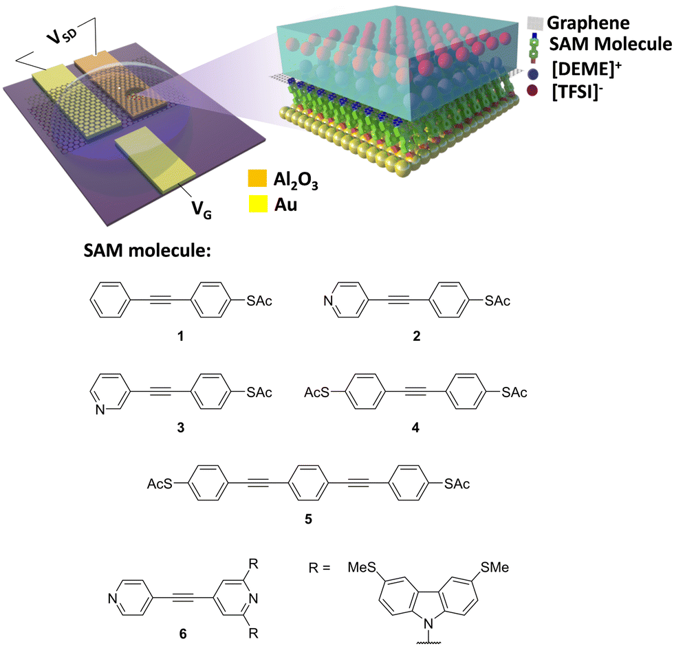 | ||
| Fig. 1 Experimental setup (top) and molecules measured in this work (bottom) (synthesis and characterizations of 1–3 and 6 were reported previously,57 synthesis and characterizations of 4 and 5 are reported in the ESI†). | ||
The current leakage through the ionic liquid was checked by measuring the I–V characteristic between drain and gate (IDG). Results indicate that in the scanning range between −1.1 V and +2 V, due to the advantage of the double-layer capacitor property of ionic liquids,61 the leakage current IDG is negligible compared with the source–drain current ISD. (Fig. S4, ESI†). Beyond this range, the leakage current increases exponentially and therefore the gate voltage used in this work was kept below this value. Furthermore, the leakage current was found to increase with time under ambient conditions, and therefore to avoid significant leakage, all measurements were carried out within 48 hours of depositing the ionic liquid.
To investigate the effect of the SAM/electrode interface on electron transport properties, 6 different molecules with OAE backbones were used for SAM fabrication (Fig. 1, bottom panel). This family of molecules have been intensively investigated because of the small gap between the highest occupied and lowest unoccupied molecular orbitals (the HOMO–LUMO gap) and their rigid unidimensional structure.62,63 Molecule 1 has an acetyl-protected thiol (SAc) terminal group at one end and is benzene terminated at the other end. Thiols are known to have strong affinity with gold, whereas benzene has negligible affinity to gold.64,65 Molecules 2 and 3 are SAc terminated at one end and have a para- or meta-connected terminal pyridine group, respectively, at the other end. Pyridine is known to have affinity to gold in either of these connectivities.4,37,66 Molecules 4 and 5 are symmetrical designs, with SAc terminal groups at both ends (in para positions). Molecule 5 contains an additional PE repeat unit compared to the other species in this study. Molecule 6 has a pyridine group at each end in the para position, and a methyl thioether (SMe)-based tetrapodal group at one end, which was used to assist self-assembly.57 Previous research has shown this tetrapodal group does not participate significantly in electron transport,57 and therefore the transmission coefficient of molecule 6 should be near-identical to an OAE terminated with two pyridines in para-positions, assuming similar backbone geometry.
The composition and assembly properties of deposited SAMs were characterized by X-ray photoelectron spectroscopy (XPS). The gold substrate was treated in the same way as for device fabrication, except that a shadow mask was not used during the lithography process. Fig. 2 shows the S2p spectra of SAMs 1–4 and 6 (the S2p spectrum for SAM 5 was identical to 4). SAM 1 can be fitted by a single doublet peak (blue curve), with S2p2/3 at 162.3 eV, which is the typical feature for a thiolate group bonded to Au.67–69 SAMs 2–4 showed features from two types of sulfur, which were fitted by two doublet peaks (blue and red). The blue curve with S2p2/3 at 162.3 (±0.03) eV indicated the thiolate bound to gold, and the red curve with S2p2/3 at 164.5 (±0.07) eV was a sign of protected thiol group not bound to the surface.64,68 The possibility of non-covalently bound (protected) thiol for SAM 1 and SAM 2 should be identical if thiol is the only anchor in each case. However, comparing the XPS results for SAM 1 and SAM 2 shows that a second set of S peaks appear only for SAM 2, thus we assign them as unbound protected thiols rather than non-covalently bound species. Based on the ratio between these two types of sulfur, we estimated the different binding motifs present within the SAMs on Au (Fig. 2, right panel). For SAM 1, only type 1 S (blue curve, S bonded to Au) was observed, which means all the molecules had grown on Au with motif a (right panel, SAM 1). For SAM 4, type 1 S and type 2 S (red curve, S non-bonded) have a ratio of 1![[thin space (1/6-em)]](https://www.rsc.org/images/entities/char_2009.gif) :1, which means all the molecules are attached to the Au substrate in a significantly tilted conformation relative to the surface normal (right panel, SAM 4), as expected with one sulfur bonded to the bottom gold and the other sulfur located at the top of the SAM in SAc form. SAMs 2 and 3 contain two functional groups capable of binding with Au, namely the S group (deprotected SAc) group and the pyridine group.64,66 For SAM 2, type 1 and type 2 S are in the ratio ∼1:1, indicating that half of the molecules in SAM 2 were bound to gold through the thiolate moiety (motif a, SAM 2) and half through the pyridine moiety (motif b, SAM 2). For a flat gold surface, this ratio is unexpected, because the thiol group has a higher binding affinity than pyridine. However, it is widely acknowledged that the pyridine binding energy to gold increases significantly if the gold surface is not flat, due to the presence of adatoms or step edges,54,55,70 as in the case of the multi-crystalline gold used here. This ratio was ∼3:1 for SAM 3, with 3/4 molecules bonded to gold by the thiolate (motif a, SAM 3) and 1/4 by pyridine (motif b, SAM 3). SAM 6 shows a single sulfur type with a position similar to SAM 1, corresponding to a SMe group bound to gold, as SMe and thiolate-based SAMs have a similar sulfur signal in XPS.71
:1, which means all the molecules are attached to the Au substrate in a significantly tilted conformation relative to the surface normal (right panel, SAM 4), as expected with one sulfur bonded to the bottom gold and the other sulfur located at the top of the SAM in SAc form. SAMs 2 and 3 contain two functional groups capable of binding with Au, namely the S group (deprotected SAc) group and the pyridine group.64,66 For SAM 2, type 1 and type 2 S are in the ratio ∼1:1, indicating that half of the molecules in SAM 2 were bound to gold through the thiolate moiety (motif a, SAM 2) and half through the pyridine moiety (motif b, SAM 2). For a flat gold surface, this ratio is unexpected, because the thiol group has a higher binding affinity than pyridine. However, it is widely acknowledged that the pyridine binding energy to gold increases significantly if the gold surface is not flat, due to the presence of adatoms or step edges,54,55,70 as in the case of the multi-crystalline gold used here. This ratio was ∼3:1 for SAM 3, with 3/4 molecules bonded to gold by the thiolate (motif a, SAM 3) and 1/4 by pyridine (motif b, SAM 3). SAM 6 shows a single sulfur type with a position similar to SAM 1, corresponding to a SMe group bound to gold, as SMe and thiolate-based SAMs have a similar sulfur signal in XPS.71
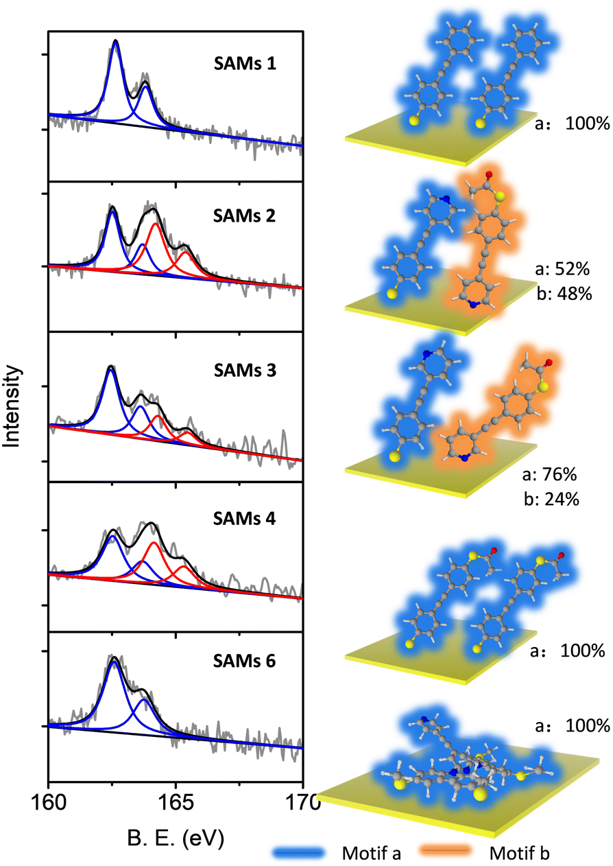 | ||
| Fig. 2 Comparison of XPS S2p spectra measured for SAMs of molecules 1–4 and 6 (5 showed identical features to 4) (left). Different binding motifs present within the SAMs on Au (right). | ||
Oxygen spectra were also recorded for all the SAMs. Oxygen signals were detected for SAMs 2–5, but not for SAMs 1 and 6. It can therefore be concluded that the oxygen signals derive from the acetyl protecting group, as SAMs 2–5 contain a SAc group not bound to the surface. This contrasts with SAM 1, where an absence of oxygen signals indicates that all S atoms from SAc groups were bound to Au and all acetate groups were cleaved during surface assembly64,72 (Fig. S7(a), ESI†). The nitrogen spectra for SAMs 1, 2 and 6 are also shown in the ESI† (Fig. S7(b and c)). SAM 1 showed no nitrogen signal as expected. SAM 2 showed a tailing nitrogen peak, which can be separated into two peaks corresponding to bound and non-bond nitrogen. SAM 6 showed two distinct peaks, with one at 399 eV corresponding to nitrogen in pyridine, and the other at 401.5 eV corresponding to nitrogen in the tetrapod anchor. The binding angle between the molecule and substrate was estimated based on the film thickness and molecular length64,73 (Table 1 and Table S4, ESI†). XPS spectra of a gold substrate with no molecular growth (treated in the same way as a device but immersed in solvent with no molecules) were also recorded as a reference (Fig. S5, ESI†) to confirm that there is no S or N contamination from photoresist or solvent.
| SAM | Tilt Angle (°) | Expt. (10−9G/G0) | Standard deviation (10−9G/G0) | Theory (10−9G/G0) EF − EDFTF = ±0.25 |
|---|---|---|---|---|
| a 42° corresponds to motif a and 68° and 16° to motif b (2 and 3, respectively). | ||||
| 1 | 42 | 5.9 | 0.37 | 9.5, 12 × 104 |
| 2 | 42/68a | 2.2 | 0.56 | 1.0, 2.7 × 10³ |
| 3 | 42/16a | 6.7 | 0.89 | 3.9, 1.9 × 10⁴ |
| 4 | 43 | 4.1 | 0.53 | 5.5, 5.0 × 10³ |
| 5 | 45 | 1.2 | 0.57 | 1.0, 1.1 × 10² |
| 6 | 40 | 1.3 | 0.15 | 4.0, 8.2 × 10² |
The electrical transport properties of the molecules were obtained from the graphene-based micro-well devices (Fig. 3a). The wells were covered with gold for SAM growth (Fig. 3b). The size of the wells was estimated by counting pixels from optical images, and further verified by atomic force microscopy (AFM) data (Table S3, ESI†). Details of the relationship between conductance and junction area are shown in Fig. S9(a–f) (ESI†), and a positive relationship between measured conductance and well area was observed. The electrodes labelled as c1 and c2 in Fig. 3 were contacts common to all junctions, as they were protected by photoresist during SAM growth and, therefore, were not covered by molecules and made good contact directly to the graphene. The in-plane conductance of graphene (GGr) was measured by applying a voltage between two common contacts, and the conductance of a SAM (GSAM) was measured by applying a voltage between the gold finger underneath the SAM in a micro-well and its nearest common contact. The junction was only considered ‘intact’ if GSAM was significantly lower than GGr, otherwise it was counted as a ‘short’. The success rate of different SAMs is listed in Table S1 (ESI†). Of the 6 molecules, SAMs of molecules 1, 3, 4 and 5 show comparable survival rates (∼55% among all junctions), and almost all the non-functioning junctions are short circuits (∼45% among all junctions). The short circuits are expected to be the result of the pin-holes and poor-quality regions in the SAMs, such as exposed gold regions, which touch with graphene directly and lead to high current flow. SAMs of molecule 2 show much lower probability of short circuits (∼23%). This could be because molecule 2 in motif b has a larger tilt angle (because the lone pair of nitrogen is orthogonal to the conjugated ring), and thus has a smaller molecular occupation area. This property helped the molecule to form highly packed SAMs and decreased the possibility of shorts. SAMs of molecule 6 show high short-circuit probabilities (65%). This was because the gold used in this work was polycrystalline and therefore the four SMe anchors of molecule 6 would not interact with gold in a uniform geometry, resulting in low SAM quality.
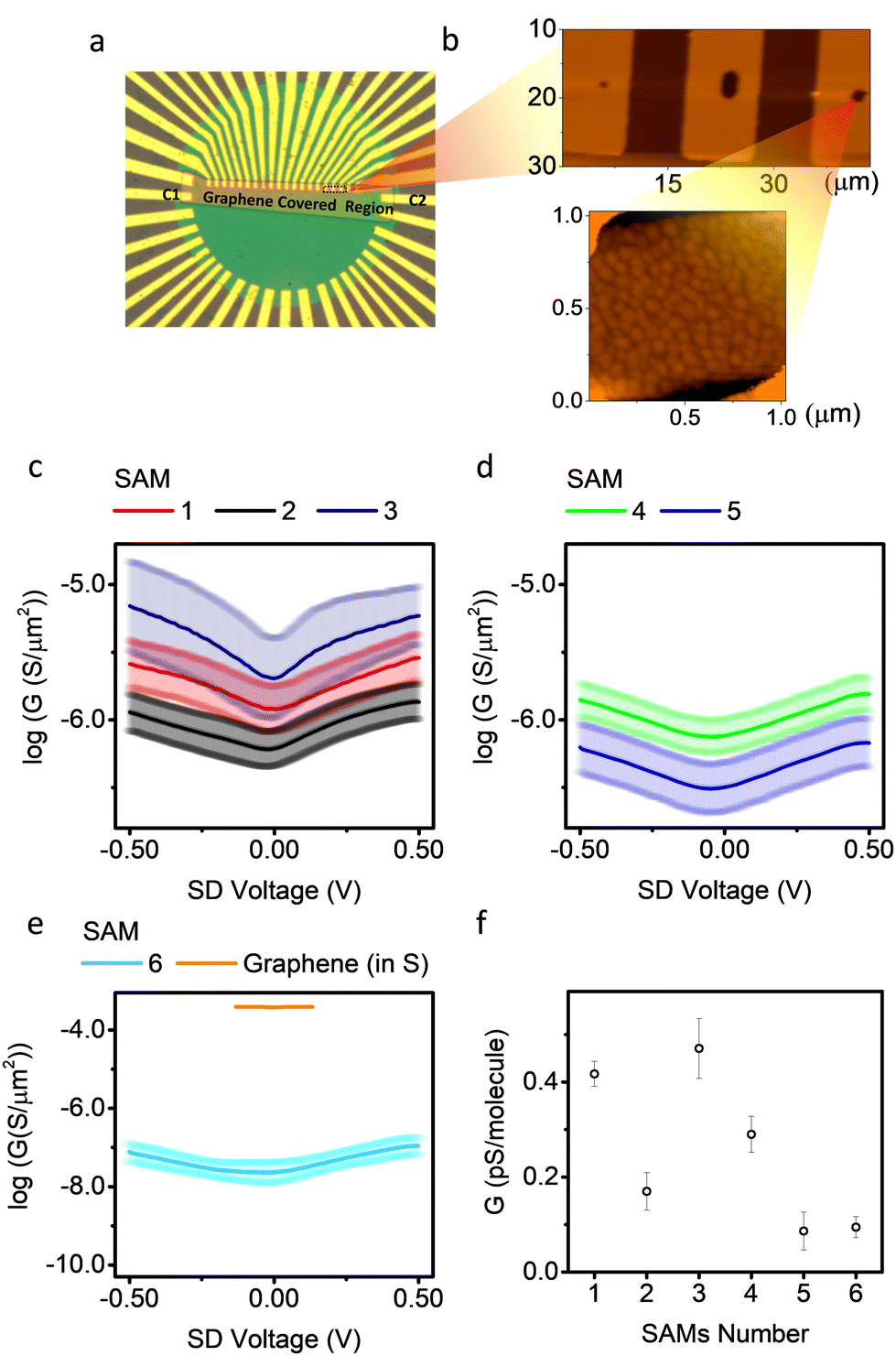 | ||
| Fig. 3 (a and b) Optical micrographs of a typical micro-well-based device used in this work. (c–e) Conductance G on a log scale vs. applied source–drain voltage for SAMs 1–5, and in-plane conductance across graphene. (f) Zero-bias conductance of molecules 1–6. | ||
Fig. 3(c) shows G–V plots on a log scale for SAMs 1, 2 and 3. SAM 1 and 2 have similar tunnelling length, but different molecule–electrode interfaces. The G–V curve of SAM 2 is the combined electric behaviour motifs a and b. Theory shows (Fig. S33, ESI†) that the junction conductance for molecule 2 with motif a is about an order of magnitude higher than motif b. This is because the coupling of thiol/Au (motif a) is stronger than pyridine/Au (motif b), resulting in a broader HOMO–LUMO gap, which increases the transmission probability around Fermi region.74 Furthermore, instead of releasing acetyl group and form thiol/Au coupling like motif a, the acetyl group for motif b was not released and remained in physical contact with the graphene top electrode. This increased the tunnelling length for motif b and decreased its conductance. SAM 1 has only one configuration similar to motif a of SAM 2 (the high conductance motif), and showed higher electrical conductance.
This increased the tunnelling length for motif b and decreased its conductance. SAM 1 has only one configuration similar to motif a of SAM 2 (the high conductance motif), and showed higher electrical conductance.
SAM 3 showed higher conductance compared with SAMs 1 and 2, with small asymmetry (rectification ratio ∼1.2). This might be due to the lower quality of SAM 3 complicating the molecule–electrode interface, because some molecule binds to Au substrate in motif b regime with small tilt angle and large occupation area thus decreasing the packing density of the SAMs. The smaller film thickness of SAM 3 compared with SAM 1 and 2 confirms this argument. Fig. 3(d) shows similar plots for SAMs 4 and 5, which have the same SAM-electrode contact but different tunnelling lengths. SAM 5 has a lower conductance than SAM 4, as expected, because SAM 5 has a longer tunnelling length. Although this β value is preliminary as it is obtained from only two data points, we note that this value is comparable to experimental values72 and theoretical predictions75 for similar junctions, where β is normally in the range 1.5–1.9 nm−1. The measured conductance for molecule 5 was (2.6 ± 1.2) × 105 S m−2 This is comparable to the reported value on similar Au/OAE3/Graphene junctions with a micro-well design (∼1.6 × 10⁵ S m−2), but using multi-layered reduced graphene oxide (rGO) as top electrode instead of single-layered CVD graphene as used here.76Fig. 3e shows the G–V plots of SAMs 6 and graphene only. The measured conductance of SAMs 1–5 were significantly higher than that of SAM 6, because the molecular occupation area for SAM 6 was significantly higher than SAM 1–5.57 All G–V curves except for SAM 3 were highly symmetrical, and plots of normalised differential conductance (NDC) versus gate voltage for SAMs 1–6 are shown in Fig. S42 (ESI†). The NDC curves for SAMs 1, 2, 4, and 5 were almost identical, which means they have similar transport behaviour. The NDC curve for SAM 6 was a parabolic shape and clearly different from SAMs 1–5. This can be explained because the large tetrapodal anchor of 6 effectively separates the molecular wires from their neighbours, thus avoiding cross talk between molecules in the SAMs which could smear out some molecular features. Fig. 3f shows a comparison of conductance of all measured SAMs, calibrated to single molecular occupation area (mean conductance per molecule) at zero bias, with the assumption that the molecular occupation area for molecules 1–5 was 0.35 nm2 and for molecule 6 was 2.6 nm2.27,57,65 Detailed conductance data with a comparison to theory are listed in Table 1. Molecules with the same backbone, but different contacts, were shown experimentally to have conductances that differ by a factor of 5 at near zero bias.
The experimentally measured mean conductance per molecule after area calibration was significantly lower than the theoretically predicted value (Table 1). We attribute this to the difference between the geometrical contact area (Ageo) and effective electrical contact area (Aelec).77–79 In this work, Ageo was used to calibrate the mean conductance per molecule. However, previous studies have reported that for large-scale molecular junctions, Aelec is normally much smaller than Ageo, with the ratio, 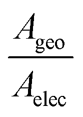 , varying from 101 to 104.77–79 In this work, a fishing method was used to transfer graphene onto the SAMs, and there is no chemical interaction between them, thus the distance between graphene and the SAMs was not well defined. It is likely that most SAM molecules will physically contact, but not electrically contact, with the graphene electrode. It is also important to notice that this work was performed on a large-scale junction. The defects induced by roughness of bottom electrode and impurities may significantly affect the electrical behaviour of SAM-based junctions.80,81 In this work thermally evaporated gold was used as a bottom electrode for SAMs growth, with relatively high surface roughness (about 1.2 nm, Fig. S15, ESI†). The “mean conductance per molecule” used in the work was averaged over a large quantity of molecules, assembled in a μm2 scale with pinholes and defects, which result in over-estimation of conductance value.
The gate dependence of different SAM-based junctions is revealed by plots of logG as a function of VG and VSD, as shown in Fig. 4. For molecules 1, 3, 4 and 5 the conductance decreases monotonically as the gate voltage is swept toward positive values in the scanned region (−0.7 V to +1.4 V). Sweeping the gate in this direction increases the density of positively charged ions next to the junction, attracting electrons to the graphene and SAM. These lower both the Fermi energy in the graphene and the molecular orbital energies, which pushes the Fermi level of the graphene closer to the LUMO resonance of the junction. The decrease in conductance implies that at zero gate voltage the Fermi level of graphene is closer to the HOMO resonance of the junction, and the Fermi level is shifted towards the off-resonance region as the molecular orbitals move down in energy. This is expected because molecules 1, 3, 4 and 5 are anchored (or mostly anchored) on gold by the thiolate group, and the lone pairs of thiolate anchors are coplanar with the π channel of the wire. Thus, the Au-lone-pair transport is π-dominated, and conductance principally occurs through the HOMO (Fig. S45, ESI†).82
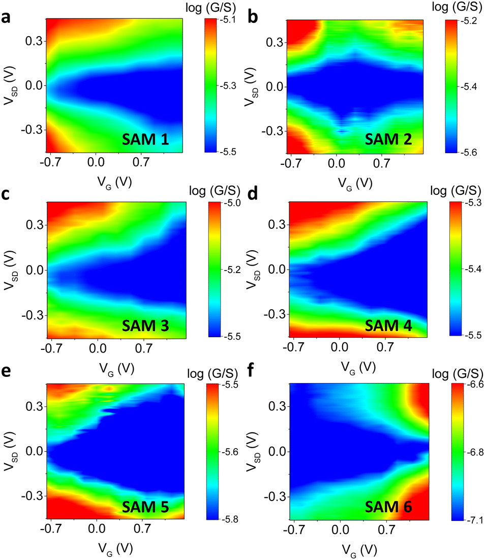 | ||
| Fig. 4 Experimental plots of logG vs. VG and VSD for SAMs 1–6 (a–f, respectively). | ||
Molecule 6 shows the opposite trend, in which the conductance increases as the gate voltage is swept from negative to positive. This means that the Fermi level is closer to the LUMO for this type of junction. In this case, the lone pair of nitrogen in pyridine is orthogonal to the π channel of the wire, so that coupling to the π* orbital is more significant and the transport is LUMO-dominated.
Molecules 2 and 5 showed an ambipolar trend, in which the molecular conductance first decreased as the gate voltage was scanned towards positive values. It then reached a minimum at a certain gate voltage (Vmin), and after that, the conductance increased, forming a diamond structure. In this case, both the HOMO and LUMO were involved in the electron transport. For molecule 2, Vmin ≈ 0.22 V, and we interpret this small value as resulting from the heterogeneity of SAMs with two different motifs (Fig. 2, SAM 2, motif a and b). It has been reported that the heterogeneous SAMs sometime have electronic structure and electric property significantly different from pure SAMs.83,84 In SAM 2, motif has Au/thiol lone-pair transport, which is π-dominated, and motif b has Au/pyridine lone-pair transport, which is π*-dominated. When combined, the net transport behaviour may not be equal to the linear sum of two types of pure motifs, but with a new energy state created,85 which results in the observed ambipolar behaviour. Vmin for molecule 5 was 1.05 V, which is consistent with a smaller HOMO–LUMO gap due to the increased length of the conjugation.
A plot of logG vs. VG and VSD for a Au/graphene/Au junction with no SAM grown on it is shown in Fig. S11 (ESI†). The result indicates that the graphene is p-doped, and the behaviour of the junction with and without a SAM is significantly different. Fig. S12 (ESI†) shows other sets of representative data of log (G) vs. VG and VSD, with details listed in Table S2 (ESI†).
Theoretical transport calculations
The transport properties of the six types of junction were modelled using a combination of density functional theory (DFT) and quantum transport theory. To calculate the electrical transport through SAMs 1–6, we modelled the three-terminal junction shown in the top panels of Fig. S31–S37 (for more details see Section 2.7 in the ESI†). The optimal binding distances between the electrodes and the different anchor groups were obtained by calculating their binding energies as a function of distance, as shown in Fig. S23–S28 (ESI†). The data are summarized in Table S5 (ESI†). The resulting transmission coefficients are shown in Fig. S32–S37 (ESI†). The results show that the transmission coefficients near the DFT-predicted Fermi energies for 1–5 are HOMO-dominated, whereas 6 is LUMO-dominated (Fig. S38, ESI†). For 2 and 3, the relative position of EF depends on whether the gold is flat or possesses a gold cluster at the molecule-gold contact (Fig. S39 and S40, ESI†), demonstrating that 2 and 3 (which have pyridyl anchors) are sensitive to the shape of the electrode. Fig. S44 (ESI†) shows the theoretical two-dimensional plots of dI/dVDvs. VG and VD for the six molecules, which are in a qualitative agreement with the experimental plots of Fig. 4. These reveal whether transport is HOMO-dominated (1, 3, 5), LUMO-dominated (3, 6) or close to the mid-gap (2), as shown in Fig. S40 (ESI†).Conclusions
In summary, we have demonstrated new procedures for gating of large-scale molecular junctions with a Au/molecules/SLG architecture by using an ionic liquid as a top gate. By applying an external gate to different types of OAE-based molecules, the tuning of the orbital alignments by altering the SAM/electrode interface and the SAM backbone structure is visualized through conductance maps varying source–drain and gate voltages. The data shed new light on the fundamental nature of electron transport within the HOMO–LUMO energy gap in molecular junctions and will be important in scaling up molecular electronic systems. The assembly and gating procedures should be versatile for junctions comprising a wide range of molecules with tailored functionality. Furthermore, this study opens new ideas for designing electronic and thermoelectric devices based on molecular thin films with potential practical applications. For example, the fact that the gate voltage can penetrate through SLG and affect the molecules beneath offers new possibilities of using graphene as a bottom electrode for SAMs with pyrene85,86 or amine87 growth, and using a back gate to realize Fermi level control.Author contributions
C. J. L., C. F., M. R. B., X. W. and A. K. I conceived the research. A. K. I., H. A. and A. A. carried out the calculations. X. W., S. N., H. A. and J. G. performed device design, fabrication and measurements. L. J. O. synthesised the molecules. All co-authors assisted in writing the manuscript. X. W., A. K. I, C. F., M. R. B. and C. J. L. supervised the research and provided essential contributions to interpreting the results and drafting the manuscript.Conflicts of interest
We declare that we have no conflict of interest.Acknowledgements
This work was supported by the UK EPSRC (grants EP/P027156/1, EP/P027172/1 and EP/P027520/1). A. K. I. acknowledges the Leverhulme Trust for Early Career Fellowship ECF-2020-638. A. K. I and C. J. L. acknowledge financial support from the UK EPSRC (grants EP/M014452/1 and EP/N03337X/1). This work was additionally funded by the European Commission FET Open projects 767187-QuIET and 766853-EFINED, and the EU project Bac-to-Fuel. H. A. is grateful for financial assistance from Taif-University (Saudi Arabia), and the Saudi Ministry of Education. A. K. I. and A. A. are grateful for financial assistance from Tikrit and Anbar Universities (Iraq), and the Iraqi Ministry of Higher Education (SL-20).References
- S. V. Aradhya and L. Venkataraman, Nat. Nanotechnol., 2013, 8, 399–410 CrossRef CAS PubMed.
- A. K. Ismael, A. Al-Jobory, I. Grace and C. J. Lambert, J. Chem. Phys., 2017, 146, 064704 CrossRef PubMed.
- C. J. Lambert, Chem. Soc. Rev., 2015, 44, 875–888 RSC.
- A. Ismael, X. T. Wang, T. L. R. Bennett, L. A. Wilkinson, B. J. Robinson, N. J. Long, L. F. Cohen and C. J. Lambert, Chem. Sci., 2020, 11, 6836–6841 RSC.
- A. J. Bergren, R. L. McCreery, S. R. Stoyanov, S. Gusarov and A. Kovalenko, J. Phys. Chem. C, 2010, 114, 15806–15815 CrossRef CAS.
- F. Evers, R. Korytár, S. Tewari and J. M. van Ruitenbeek, Rev. Mod. Phys., 2020, 92, 035001 CrossRef CAS.
- M. T. González, A. K. Ismael, M. Garcia-Iglesias, E. Leary, G. Rubio-Bollinger, I. Grace, D. Gonzalez-Rodriguez, T. Torres, C. J. Lambert and N. Agrait, J. Phys. Chem. C, 2021, 125, 15035–15043 CrossRef.
- G. J. Ashwell, B. Urasinska, C. S. Wang, M. R. Bryce, I. Grace and C. J. Lambert, Chem. Commun., 2006, 45, 4706–4708 RSC.
- A. Aviram and M. A. Ratner, Bull. Am. Phys. Soc., 1974, 19, 341 Search PubMed.
- S. Naghibi, A. K. Ismael, A. Vezzoli, M. K. Al-Khaykanee, X. Zheng, I. M. Grace, D. Bethell, S. J. Higgins, C. J. Lambert and R. J. Nichols, J. Phys. Chem. Lett., 2019, 10, 6419–6424 CrossRef CAS PubMed.
- C. J. Lambert, Quantum Transport in Nanostructures and Molecules, IOP Publishing, 2021 Search PubMed.
- S. Park, H. R. Kim, J. Kim, B. H. Hong and H. J. Yoon, Adv. Mater., 2021, 33, 2103177 CrossRef CAS PubMed.
- S. Park and H. J. Yoon, Nano Lett., 2018, 18, 7715–7718 CrossRef CAS PubMed.
- M. Carlotti, S. Soni, S. Kumar, Y. Ai, E. Sauter, M. Zharnikov and R. C. Chiechi, Angew. Chem., Int. Ed., 2018, 57, 15681–15685 CrossRef CAS PubMed.
- F. B. Meng, Y. M. Hervault, Q. Shao, B. H. Hu, L. Norel, S. Rigaut and X. D. Chen, Nat. Commun., 2014, 5, 3023 CrossRef PubMed.
- S. Kumar, M. Merelli, W. Danowski, P. Rudolf, B. L. Feringa and R. C. Chiechi, Adv. Mater., 2019, 31, 1807831 CrossRef PubMed.
- N. Xin, X. X. Li, C. C. Jia, Y. Gong, M. L. Li, S. P. Wang, G. Y. Zhang, J. L. Yang and X. F. Guo, Angew. Chem., Int. Ed., 2018, 57, 14026–14031 CrossRef CAS PubMed.
- X. Wang, A. Ismael, A. Almutlg, M. Alshammari, A. Al-Jobory, A. Alshehab, T. L. Bennett, L. A. Wilkinson, L. F. Cohen and N. J. Long, Chem. Sci., 2021, 12, 5230–5235 RSC.
- N. Xin, J. X. Guan, C. G. Zhou, X. J. N. Chen, C. H. Gu, Y. Li, M. A. Ratner, A. Nitzan, J. F. Stoddart and X. F. Guo, Nat. Rev. Phys., 2019, 1, 211–230 CrossRef.
- X. K. Qiu, V. Ivasyshyn, L. Qiu, M. Enache, J. J. Dong, S. Rousseva, G. Portale, M. Stohr, J. C. Hummelen and R. C. Chiechi, Nat. Mater., 2020, 19, 330–337 CrossRef CAS PubMed.
- C. A. Martin, D. Ding, J. K. Sorensen, T. Bjornholm, J. M. van Ruitenbeek and H. S. J. van der Zant, J. Am. Chem. Soc., 2008, 130, 13198–13199 CrossRef CAS PubMed.
- A. K. Ismael, L. Rincón-García, C. Evangeli, P. Dallas, T. Alotaibi, A. A. Al-Jobory, G. Rubio-Bollinger, K. Porfyrakis, N. Agraït and C. J. Lambert, Nanoscale Horiz., 2022, 7, 616–625 RSC.
- T. Hines, I. Diez-Perez, J. Hihath, H. M. Liu, Z. S. Wang, J. W. Zhao, G. Zhou, K. Muellen and N. J. Tao, J. Am. Chem. Soc., 2010, 132, 11658–11664 CrossRef CAS PubMed.
- J. C. Love, L. A. Estroff, J. K. Kriebel, R. G. Nuzzo and G. M. Whitesides, Chem. Rev., 2005, 105, 1103–1169 CrossRef CAS PubMed.
- M. A. Reed, C. Zhou, C. J. Muller, T. P. Burgin and J. M. Tour, Science, 1997, 278, 252–254 CrossRef CAS.
- A. Markin, A. K. Ismael, R. J. Davidson, D. C. Milan, R. J. Nichols, S. J. Higgins, C. J. Lambert, Y.-T. Hsu, D. S. Yufit and A. Beeby, J. Phys. Chem. C, 2020, 124, 6479–6485 CrossRef CAS.
- M. Carlotti, A. Kovalchuk, T. Wachter, X. K. Qiu, M. Zharnikov and R. C. Chiechi, Nat. Commun., 2016, 7, 13904 CrossRef CAS PubMed.
- A. K. Ismael, I. Grace and C. J. Lambert, Nanoscale, 2015, 7, 17338–17342 RSC.
- M. K. Al-Khaykanee, A. K. Ismael, I. Grace and C. J. Lambert, RSC Adv., 2018, 8, 24711–24715 RSC.
- A. K. Ismael, I. Grace and C. J. Lambert, Phys. Chem. Chem. Phys., 2017, 19, 6416–6421 RSC.
- Y. X. Zhang, Z. Y. Zhao, D. Fracasso and R. C. Chiechi, Isr. J. Chem., 2014, 54, 513–533 CrossRef CAS.
- N. Nerngchamnong, L. Yuan, D. C. Qi, J. Li, D. Thompson and C. A. Nijhuis, Nat. Nanotechnol., 2013, 8, 113–118 CrossRef CAS PubMed.
- A. J. Kronemeijer, H. B. Akkerman, T. Kudernac, B. J. van Wees, B. L. Feringa, P. W. M. Blom and B. de Boer, Adv. Mater., 2008, 20, 1467–1473 CrossRef CAS.
- A. K. Ismael and C. J. Lambert, J. Mater. Chem. C, 2019, 7, 6578–6581 RSC.
- O. A. Al-Owaedi, D. C. Milan, M. C. Oerthel, S. Bock, D. S. Yufit, J. A. K. Howard, S. J. Higgins, R. J. Nichols, C. J. Lambert, M. R. Bryce and P. J. Low, Organometallics, 2016, 35, 2944–2954 CrossRef CAS.
- L. Herrer, A. Ismael, S. Martin, D. C. Milan, J. L. Serrano, R. J. Nichols, C. Lambert and P. Cea, Nanoscale, 2019, 11, 15871–15880 RSC.
- A. Ismael, A. Al-Jobory, X. T. Wang, A. Alshehab, A. Almutlg, M. Alshammari, I. Grace, T. L. R. Benett, L. A. Wilkinson, B. J. Robinson, N. J. Long and C. Lambert, Nanoscale Adv., 2020, 2, 5329–5334 RSC.
- V. Kaliginedi, A. V. Rudnev, P. Moreno-Garcia, M. Baghernejad, C. C. Huang, W. J. Hong and T. Wandlowski, Phys. Chem. Chem. Phys., 2014, 16, 23529–23539 RSC.
- C. H. He, Q. Zhang, Y. Q. Fan, C. Z. Zhao, C. Zhao, J. Y. Ye, Y. J. Dappe, R. J. Nichols and L. Yang, Chem. Phys. Chem., 2019, 20, 1830–1836 CrossRef CAS PubMed.
- I. L. Herrer, A. K. Ismael, D. C. Milan, A. Vezzoli, S. Martín, A. González-Orive, I. Grace, C. Lambert, J. L. Serrano and R. J. Nichols, J. Phys. Chem. Lett., 2018, 9, 5364–5372 CrossRef CAS PubMed.
- R. Frisenda, S. Tarkuc, E. Galan, M. L. Perrin, R. Eelkema, F. C. Grozema and H. S. J. van der Zant, Beilstein J. Nanotechnol., 2015, 6, 1558–1567 CrossRef CAS PubMed.
- A. K. Ismael and C. J. Lambert, Nanoscale Horiz., 2020, 5, 1073–1080 RSC.
- F. Chen, X. L. Li, J. Hihath, Z. F. Huang and N. J. Tao, J. Am. Chem. Soc., 2006, 128, 15874–15881 CrossRef CAS PubMed.
- V. Meded, A. Bagrets, A. Arnold and F. Evers, Small, 2009, 5, 2218–2223 CrossRef CAS PubMed.
- Y. Q. Li, M. Buerkle, G. F. Li, A. Rostamian, H. Wang, Z. X. Wang, D. R. Bowler, T. Miyazaki, L. M. Xiang, Y. Asai, G. Zhou and N. J. Tao, Nat. Mater., 2019, 18, 357–363 CrossRef CAS PubMed.
- A. W. Ghosh, T. Rakshit and S. Datta, Nano Lett., 2004, 4, 565–568 CrossRef CAS.
- M. Famili, C. C. Jia, X. S. Liu, P. Q. Wang, I. M. Grace, J. Guo, Y. Liu, Z. Y. Feng, Y. L. Wang, Z. P. Zhao, S. Decurtins, R. Haner, Y. Huang, S. X. Liu, C. J. Lambert and X. F. Duan, Chemistry, 2019, 5, 474–484 CrossRef CAS.
- C. C. Jia, M. Famili, M. Carlotti, Y. Liu, P. Q. Wang, I. M. Grace, Z. Y. Feng, Y. L. Wang, Z. P. Zhao, M. N. Ding, X. Xu, C. Wang, S. J. Lee, Y. Huang, R. C. Chiechi, C. J. Lambert and X. F. Duan, Sci. Adv., 2018, 4, eaat8237 CrossRef CAS PubMed.
- G. Wang, Y. Kim, M. Choe, T. W. Kim and T. Lee, Adv. Mater., 2011, 23, 755–760 CrossRef CAS PubMed.
- L. Britnell, R. V. Gorbachev, R. Jalil, B. D. Belle, F. Schedin, A. Mishchenko, T. Georgiou, M. I. Katsnelson, L. Eaves, S. V. Morozov, N. M. R. Peres, J. Leist, A. K. Geim, K. S. Novoselov and L. A. Ponomarenko, Science, 2012, 335, 947–950 CrossRef CAS PubMed.
- T. Georgiou, R. Jalil, B. D. Belle, L. Britnell, R. V. Gorbachev, S. V. Morozov, Y. J. Kim, A. Gholinia, S. J. Haigh, O. Makarovsky, L. Eaves, L. A. Ponomarenko, A. K. Geim, K. S. Novoselov and A. Mishchenko, Nat. Nanotechnol., 2013, 8, 100–103 CrossRef CAS PubMed.
- T. Tian, P. Rice, E. J. G. Santos and C. J. Shih, Nano Lett., 2016, 16, 5044–5052 CrossRef CAS PubMed.
- P. Q. Wang, C. C. Jia, Y. Huang and X. F. Duan, Matter, 2021, 4, 552–581 CrossRef CAS.
- R. Stadler, K. S. Thygesen and K. W. Jacobsen, Phys. Rev. B: Condens. Matter Mater. Phys., 2005, 72, 241401 CrossRef.
- S. M. Hou, J. X. Zhang, R. Li, J. Ning, R. S. Han, Z. Y. Shen, X. Y. Zhao, Z. Q. Xue and Q. Wu, Nanotechnology, 2005, 16, 239–244 CrossRef CAS PubMed.
- D. Z. Manrique, C. Huang, M. Baghernejad, X. T. Zhao, O. A. Al-Owaedi, H. Sadeghi, V. Kaliginedi, W. J. Hong, M. Gulcur, T. Wandlowski, M. R. Bryce and C. J. Lambert, Nat. Commun., 2015, 6, 6389 CrossRef CAS PubMed.
- L. J. O'Driscoll, X. T. Wang, M. Jay, A. S. Batsanov, H. Sadeghi, C. J. Lambert, B. J. Robinson and M. R. Bryce, Angew. Chem., Int. Ed., 2020, 59, 882–889 CrossRef PubMed.
- T. Li, M. Jevric, J. R. Hauptmann, R. Hviid, Z. M. Wei, R. Wang, N. E. A. Reeler, E. Thyrhaug, S. Petersen, J. A. S. Meyer, N. Bovet, T. Vosch, J. Nygard, X. H. Qiu, W. P. Hu, Y. Q. Liu, G. C. Solomon, H. G. Kjaergaard, T. Bjornholm, M. B. Nielsen, B. W. Laursen and K. Norgaard, Adv. Mater., 2013, 25, 4164–4170 CrossRef CAS PubMed.
- Z. R. Wang, H. L. Dong, T. Li, R. Hviid, Y. Zou, Z. M. Wei, X. L. Fu, E. J. Wang, Y. G. Zhen, K. Norgaard, B. W. Laursen and W. P. Hu, Nat. Commun., 2015, 6, 8237 CrossRef PubMed.
- Y. Jang, H. Jeong, D. Kim, W. T. Hwang, J. W. Kim, I. Jeong, H. Song, J. Yoon, G. C. Yi, H. Jeong and T. Lee, Nanotechnology, 2016, 27, 145301 CrossRef PubMed.
- U. Ulissi, G. A. Elia, S. Jeong, F. Mueller, J. Reiter, N. Tsiouvaras, Y. K. Sun, B. Scrosati, S. Passerini and J. Hassoun, ChemSusChem, 2018, 11, 229–236 CrossRef CAS PubMed.
- Y. Li, J. Zhao and G. Yin, Comput. Mater. Sci., 2007, 39, 775–781 CrossRef CAS.
- L. J. O'Driscoll and M. R. Bryce, Nanoscale, 2021, 10668–10711 RSC.
- Z. M. Wei, T. Li, K. Jennum, M. Santella, N. Bovet, W. P. Hu, M. B. Nielsen, T. Bjornholm, G. C. Solomon, B. W. Laursen and K. Norgaard, Langmuir, 2012, 28, 4016–4023 CrossRef CAS PubMed.
- Z. M. Wei, T. Hansen, M. Santella, X. T. Wang, C. R. Parker, X. B. Jiang, T. Li, M. Glyvradal, K. Jennum, E. Glibstrup, N. Bovet, X. W. Wang, W. P. Hu, G. C. Solomon, M. B. Nielsen, X. H. Qiu, T. Bjornholm, K. Norgaard and B. W. Laursen, Adv. Funct. Mater., 2015, 25, 1700–1708 CrossRef CAS.
- Z. Y. Ma, F. Rissner, L. J. Wang, G. Heimel, Q. K. Li, Z. G. Shuai and E. Zojer, Phys. Chem. Chem. Phys., 2011, 13, 9747–9760 RSC.
- T. B. Creczynski-Pasa, M. A. D. Millone, M. L. Munford, V. R. de Lima, T. O. Vieira, G. A. Benitez, A. A. Pasa, R. C. Salvarezza and M. E. Vela, Phys. Chem. Chem. Phys., 2009, 11, 1077–1084 RSC.
- C. Vericat, M. E. Vela, G. Benitez, P. Carro and R. C. Salvarezza, Chem. Soc. Rev., 2010, 39, 1805–1834 RSC.
- T. Ishida, N. Nishida, S. Tsuneda, M. Hara, H. Sasabe and W. Knoll, Jpn. J. Appl. Phys., Part 2, 1996, 35, L1710–L1713 CrossRef CAS.
- S. Y. Quek, M. Kamenetska, M. L. Steigerwald, H. J. Choi, S. G. Louie, M. S. Hybertsen, J. B. Neaton and L. Venkataraman, Nat. Nanotechnol., 2009, 4, 230–234 CrossRef CAS PubMed.
- M. S. Inkpen, Z. F. Liu, H. Li, L. M. Campos, J. B. Neaton and L. Venkataraman, Nat. Chem., 2019, 11, 351–358 CrossRef CAS PubMed.
- H. Valkenier, E. H. Huisman, P. A. van Hal, D. M. de Leeuw, R. C. Chiechi and J. C. Hummelen, J. Am. Chem. Soc., 2011, 133, 4930–4939 CrossRef CAS PubMed.
- C. D. Bain and G. M. Whitesides, J. Phys. Chem., 1989, 93, 1670–1673 CrossRef CAS.
- G. Berdiyorov and H. Hamoudi, J. Mater. Res. Technol., 2021, 12, 193–201 CrossRef CAS.
- H. M. Liu, N. Wang, J. W. Zhao, Y. Guo, X. Yin, F. Y. C. Boey and H. Zhang, Chem. Phys. Chem., 2008, 9, 1416–1424 CrossRef CAS PubMed.
- T. Li, J. R. Hauptmann, Z. M. Wei, S. Petersen, N. Bovet, T. Vosch, J. Nygard, W. P. Hu, Y. Q. Liu, T. Bjornholm, K. Norgaard and B. W. Laursen, Adv. Mater., 2012, 24, 1333–1339 CrossRef CAS PubMed.
- S. K. Karuppannan, E. H. L. Neoh, A. Vilan and C. A. Nijhuis, J. Am. Chem. Soc., 2020, 142, 3513–3524 CrossRef CAS PubMed.
- S. Mukhopadhyay, S. K. Karuppannan, C. L. Guo, J. A. Fereiro, A. Bergren, V. Mukundan, X. K. Qiu, O. E. C. Ocampo, X. P. Chen, R. C. Chiechi, R. McCreery, I. Pecht, M. Sheves, R. R. Pasula, S. Lim, C. A. Nijhuis, A. Vilan and D. Cahen, iScience, 2020, 23, 101099 CrossRef CAS PubMed.
- F. C. Simeone, H. J. Yoon, M. M. Thuo, J. R. Barber, B. Smith and G. M. Whitesides, J. Am. Chem. Soc., 2013, 135, 18131–18144 CrossRef CAS PubMed.
- C. S. Sangeeth, L. Jiang and C. A. Nijhuis, RSC Adv., 2018, 8, 19939–19949 RSC.
- X. Chen, H. Hu, J. Trasobares and C. A. Nijhuis, ACS Appl. Mater. Interfaces, 2019, 11, 21018–21029 CrossRef CAS PubMed.
- T. A. Su, M. Neupane, M. L. Steigerwald, L. Venkataraman and C. Nuckolls, Nat. Rev. Mater., 2016, 1, 16002 CrossRef CAS.
- F. Rissner, D. A. Egger, L. Romaner, G. Heimel and E. Zojer, ACS Nano, 2010, 4, 6735–6746 CrossRef CAS PubMed.
- G. D. Kong, S. E. Byeon, S. Park, H. Song, S. Y. Kim and H. J. Yoon, Adv. Electron. Mater., 2020, 6, 1901157 CrossRef CAS.
- H. Sadeghi, S. Sangtarash and C. Lambert, Nano Lett., 2017, 17, 4611–4618 CrossRef CAS PubMed.
- B. Limburg, J. O. Thomas, G. Holloway, H. Sadeghi, S. Sangtarash, I. C. Y. Hou, J. Cremers, A. Narita, K. Mullen, C. J. Lambert, G. A. D. Briggs, J. A. Mol and H. L. Anderson, Adv. Funct. Mater., 2018, 28, 1803629 CrossRef.
- P. Song, C. S. S. Sangeeth, D. Thompson, W. Du, K. P. Loh and C. A. Nijhuis, Adv. Mater., 2016, 28, 631–639 CrossRef CAS PubMed.
Footnotes |
| † Electronic supplementary information (ESI) available. See DOI: https://doi.org/10.1039/d2nh00241h |
| ‡ These authors contributed equally to this work. |
| This journal is © The Royal Society of Chemistry 2022 |