DOI:
10.1039/D2NH00229A
(Review Article)
Nanoscale Horiz., 2022,
7, 1029-1046
Performance optimization strategies of halide perovskite-based mechanical energy harvesters
Received
6th May 2022
, Accepted 14th June 2022
First published on 15th June 2022
Abstract
Halide perovskites, possessing unique electronic and photovoltaic properties, have been intensively investigated over the past decade. The excellent polarization, piezoelectricity, dielectricity and photoelectricity of halide perovskites provide new opportunities for the applications of mechanical energy harvesting. Although various studies have been conducted to develop halide perovskite-based triboelectric and piezoelectric nanogenerators, strategies for their electrical performance optimization are rarely mentioned. In this review, we systematically introduce the recent research progress of halide perovskite-based mechanical energy harvesters and summarize the different optimization strategies for improving both the piezoelectric and triboelectric output of the devices, bringing some inspiration to guide future material and structure design for halide perovskite-based energy devices. A summary of the current challenges and future perspectives is also presented, offering some possible directions for development in this emerging field.

Feng Jiang
| Feng Jiang is pursuing a PhD Degree at the School of Materials Science and Engineering, Nanyang Technological University (Singapore). He received his MS Degree in Chemical Engineering from Xiamen University (Xiamen, Fujian, China) in 2020. His main research interests are the design and fabrication of halide perovskite-based energy harvesters. |

Pooi See Lee
| Professor Lee Pooi See is the Dean, Graduate College and Associate Provost (Graduate Education) at Nanyang Technological University (NTU), Singapore. Her current research focuses on soft electronics, mechanical energy harvesters, human-machine interfaces, sensors and actuators, wearable technology, and hybrid materials for soft robotics. She has received many accolades such as the National Research Foundation Investigatorship, Nanyang Research Award, SNIC-AsCA2019 Distinguished Woman Chemist Award 2022. She was elected the National Academy of Inventors Fellow in 2020 and MRS Fellow 2022. |
1. Introduction
With the demanding requirements of environmental protection and low carbon emission, sustainable and clean energy, such as hydrogen, solar, water and geothermal energy, is highly desirable to serve as the main power source to accommodate the various activities of human beings, which can prominently alleviate environmental pollution and global warming. Among different forms of energy, mechanical energy is a prospective one due to its diverse sources (wind, rain, tidal energy and human motion) and flexible utilization modes. As promising techniques for collecting mechanical energy from the environment and human bodies, piezoelectric and triboelectric nanogenerators (PENGs and TENGs) are good candidates to realize self-powered functions for small electronic devices, providing a portable and flexible power source for wearable electronics and smart sensors.1–5 PENGs generate electricity via a piezoelectric effect where the charge will accumulate in response to the external stress, while TENGs transform the mechanical energy into electricity through triboelectrification and electrostatic induction effects.6,7 Both techniques are effective power sources to achieve the demands of green and sustainable energy.
Recently, halide perovskites, emerging as star materials in the field of solar cells,8 light-emitting diodes9 (LEDs) and photodetectors,10 have displayed attractive performance such as high power conversion efficiency, external quantum efficiency and photoluminescence quantum yield, due to their excellent charge carrier mobility, long carrier diffusion length, high adsorption coefficient, tunable bandgap as well as simple solution-based processing methods.11–13 Apart from these applications, halide perovskites also exhibit outstanding piezoelectric and triboelectric properties in view of their special structural and electronic properties, spontaneous polarization, as well as remarkable dielectric features.14,15 Therefore, developing halide perovskite-based mechanical energy harvesters is a promising direction for portable power sources and flexible electronics.
Some representative review papers about halide perovskite-based PENGs have previously been reported.16–18 For these reviews, emphasis has been placed on the fundamental properties, materials synthesis, energy harvesting applications and various impact factors on the output performance of halide perovskites. However, a systematic strategy for materials design and performance optimization of halide perovskite-based mechanical energy harvesters, not only on piezoelectric but including triboelectric, has not been proposed, which is significant to guide the future design of high-performance halide perovskite-based mechanical energy harvesters. In this review, we not only present the state-of-art progress in halide perovskite-based PENG and TENG devices but also pay more attention to their performance optimization strategies. The current challenges and future perspectives of halide perovskite-based mechanical energy harvesters are also discussed, offering possible directions for improving the electric performance and extending the applications of the halide perovskite-based multifunctional energy devices.
2. Crystal structure of halide perovskites
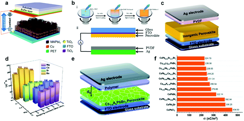
Perovskite, a term derived from Count Lev Aleksevich von Perovski who discovered the structure of calcium titanate (CaTiO3) mineral, represents a class of compounds with similar crystal structures in the form of ABX3.19 For typical three-dimensional (3D) halide perovskites, A is the monovalent cation, such as Cs+, CH3NH3+ (MA+) and CH(NH2)2+ (FA+), and B denotes the divalent cation, such as Pb2+, Sn2+, Cu2+, Ge2+ and Mn2+, while X represents the halide anions including Cl−, Br−, and I−. As shown in Fig. 1a, for a single unit cell, B cation is connected with six X anions to form a [BX6]4− octahedra structure, while the A cation will be incorporated into the body center of the cubic structure, coordinating with twelve neighboring X anions.20 The crystal formation and stability of 3D halide perovskites are usually estimated by the Goldschmidt tolerance factor t and octahedral factor μ described in the following equations:21,22| |  | (1) |
| |  | (2) |
where rA, rB, and rX represent the radii of ionic A, B and X. To maintain a stable perovskite structure, t and μ should distribute in the range of 0.81–1.11 and 0.44–0.90, respectively.21,22 In particular, the calculated t range for the ideal cubic structure of perovskites is determined to be 0.9–1, while the crystal geometry will transform to distorted (e.g. orthorhombic, tetragonal and rhombohedral) or hexagonal structures when t is lower than 0.9 or higher than 1.21–23
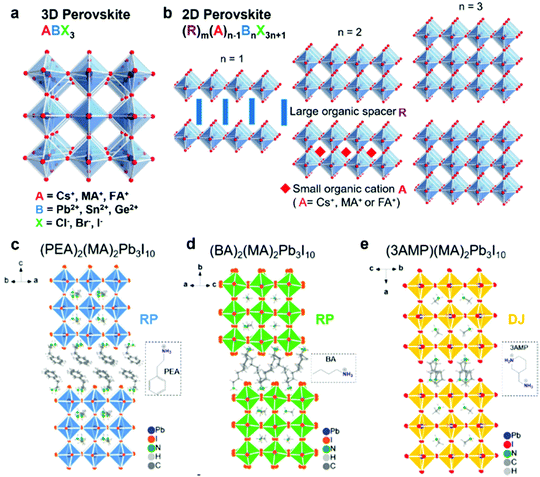 |
| | Fig. 1 Schematic illustration of 3D and 2D halide perovskite structures. (a) Schematic illustration of the typical 3D halide perovskite structure (ABX3). (b) Schematic illustration of a 2D halide perovskite structure (RmAn−1BnX3n+1) with a different number of stacked octahedral layers. Typical RP perovskites of (c) (PEA)2(MA)2Pb3I10 and (d) (BA)2(MA)2Pb3I10 (n = 3), and DJ perovskite of (e) (3AMP)2(MA)2Pb3I10 (n = 3). Reproduced with permission from ref. 20. Copyright 2019, American Chemical Society. | |
Recently, two-dimensional (2D) halide perovskites have attracted tremendous interest because they are structurally “encapsulated” by the large organic cations, preventing the invasion of ambient moisture and oxygen and thus enhancing the environmental stability compared to the traditional 3D perovskties.24,25 Notably, 2D halide perovskites break the restrictions of the Goldschmidt tolerance factor and allow large cations to be embedded into the crystal structure.20 They are considered as the structures of one or few layers exfoliated from a specific plane of their parent 3D framework, which can be described as RmAn−1BnX3n+1, where R is the large organic cation spacer; m equals 1 or 2 when R is divalent or monovalent cation; n indicates the number of stacked octahedral layers; and A, B and X represent the same ions with the previous 3D halide perovskites. Generally, a pure 2D halide perovskite will form when n equals 1 and it will transform to a standard 3D structure when n equals to ∞. The quasi-2D perovskite will be constructed when n is between 1 and ∞.20 Among different 2D perovskites, Ruddlesden–Popper (RP) and Dion–Jacobson (DJ) phase types are the most popular ones which have been extensively investigated.26,27 For RP phase perovskites, they contain two long-chain monovalent cations (m = 2) with hydrophobic groups, which can separate different perovskite layers. The various layers will connect through van der Waals interactions and the large organic cations will play an imperative function in dielectric and insulating performance, enabling perovskites with improved electronic properties and stability.28,29 In contrast to RP phase perovskites, the R site of DJ phase perovskites is replaced by a divalent cation spacer (m = 1), which can form stronger hydrogen bonding among different layers, leading to better carrier transfer properties and structural stability.30 2D halide perovskites enormously expand the types and flexibility of the current crystal structures, bringing new opportunities to molecular design and structural engineering.31
3. Halide perovskite-based piezoelectric nanogenerators
3.1. Introduction
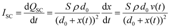
Piezoelectricity, discovered by Jacques and Pierre Curie in 1880, describes a phenomenon of electrical charge accumulation in certain materials induced by applying an external force, representing a coupling effect between mechanical and electric fields. In general, the prerequisite for piezoelectricity is that the material structures should be non-centrosymmetric, meaning the centers of the positive and negative ions should not coincide under the applied force. Therefore, a net dipole will form along a specific direction, leading to the accumulated charge. The piezoelectricity of the materials can be evaluated by their piezoelectric strain coefficient (d33). Typically, d33 can be obtained using piezoresponse force microscopy (PFM) or a static piezoelectric constant measuring system, and it quantifies the strain of a piezoelectric material under an electric field (d33 = S/E, where S and E represent the strain and electric field in the perpendicular direction). Piezoelectric voltage coefficient (g33) is another important parameter that can reflect the voltage and energy output of a piezoelectric material under a mechanical force, as shown in eqn (3).32where ε0 and εr are the vacuum permittivity and dielectric permittivity, respectively. Both d33 and g33 are significant parameters to determine the electrical output of piezoelectric nanogenerators, as illustrated in eqn (4)–(6).32,33| | 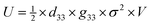 | (6) |
where Voc, σ, l, Isc, F, t, U and V represent the output voltage, stress in the perpendicular direction, device thickness, output current, applied force, time, output energy, and volume of the piezoelectric material, respectively. From these equations, the output voltage of the PENGs should increase with the reduction of dielectric constant. However, some experimental results also showed that the piezoelectric materials with a large dielectric constant could exhibit a high voltage output.34–37 This is because the increase of d33 is typically associated with the enhancement of dielectric constant, which is also the reason why it is challenging to simultaneously obtain piezoelectric materials with high d33 and g33 values.38–40 In addition, it is believed that the dielectric constant is also related to the piezoelectric polarization,41 microstructure,42 and the electromechanical coupling effect of the materials,41 so more efforts should be made to investigate the relationship among these parameters to construct a more comprehensive theory on how to achieve the high d33 and g33, simultaneously.
PENG was firstly discovered in zinc oxide nanowires by Wang et al. in 2006.6 Since then, tremendous studies have been investigated to explore the material space, structural engineering, working principle, and performance enhancement of PENG devices.43–45 Halide perovskites, as a new class of piezoelectric materials, exhibit marvelous ferroelectric and piezoelectric performance, which are comparable to the inorganic piezoelectric ceramics, such as lead zirconate titanate (PZT) and barium titanate (BTO).46 Kim et al. reported the first flexible halide perovskite-based PENG (HP-PENG) by using a MAPbI3 thin film sandwiched between two electrode-coated polyethylene terephthalate (PET) substrates through polydimethylsiloxane (PDMS) adhesion.47 The piezoelectricity of the perovskite has been proved by the ferroelectric polarization–electric field (P–E) hysteresis loop and PFM. Under the poling electrical field of 80 V μm−1, the PENG device displayed an electrical output of 2.7 V and 140 nA cm−2, which were almost three times higher than the non-poled device. The working mechanism of HP-PENG can be explained in Fig. 2a.47 The device would maintain a neutral state when no pressure was applied to it. As an external force was induced to the device, the halide perovskites would deform, rendering the charges to accumulate on the surface, so a piezoelectric potential would form between the two electrodes. To balance the electrical potential, the electrons would flow from the bottom to the top electrode via an external load, generating the instantaneous current. When the force was released, the piezoelectric potential would vanish, so the accumulated electrons would flow back and generate the current in the opposite direction. The continuous current can be produced by repeating these procedures. Notably, the piezoelectric output was small for a non-poled device because the polarization domains were randomly distributed at the initial state, so the piezoelectric performance was low under the applied force. On the contrary, all the polarization domains would align along the electrical field under the high poling voltage, leading to more charge accumulation on the surface, thus the piezoelectric output will be eminently enhanced. Xiong's group reported a manganese-based halide perovskite TMCM-MnCl3 with a d33 of 185 pm V−1 as shown in Fig. 2c, which is comparable or even better than most conventional piezoelectric materials (Fig. 2b and c).48 Then they designed a new perovskite (TMFM)x(TMCM)1–xCdCl3 with extremely high d33 that is up to ∼1540 pm V−1 (Fig. 2d), which was the highest value among halide perovskites for now.46 Despite the promising progress, the design strategies for improving HP-PENG are rarely mentioned, so a systematic theoretical model should be constructed to guide the possible optimization directions. Based on the Maxwell's displacement current, Wang's group built up a reliable model to reflect the factors affecting the electrical output of PENG.49,50 When no external electrical field is applied and the polarization is along the perpendicular direction, the output voltage and current of PENG can be described as follows:
| |  | (8) |
where
z,
σp and
ε represent the strain in the perpendicular direction, the density of the piezoelectric polarization charges on the material, and the dielectric constant of the piezoelectric material. From the equations, the density of polarization charges is the most important factor that contributes to both piezoelectric voltage and current, while the strain is another property that can enhance the electrical performance. In this case, some possible boosting methods, such as halide perovskite composition optimization, synergetic electrical enhancement by mixing with piezoelectric polymers, morphological regulation and multiaxial ferroelectric perovskite design, are promising strategies that can improve both polarization and mechanical strain.
 |
| | Fig. 2 The working mechanism of HP-PENGs and two typical halide perovskites with high piezoelectricity. (a) The working mechanism of the MAPbI3-based PENG device under non-poled and poled conditions. Reproduced with permission from ref. 47. Copyright 2016, Royal Society of Chemistry. (b) A comparison of piezoelectric strain coefficients for different piezoelectric materials. (c) Crystal structure of TMCM-MnCl3 at its ferroelectric phase. Reproduced with permission from ref. 48. Copyright 2017, American Association for the Advancement of Science. (d) Crystal structure of (TMFM)0.26(TMCM)0.74CdCl3 at its ferroelectric phase. Reproduced with permission from ref. 46. Copyright 2019, American Association for the Advancement of Science. | |
3.2. Composition optimization of halide perovskites
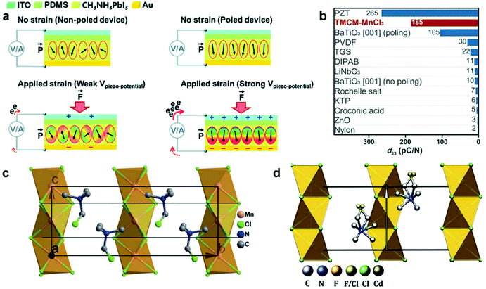
Perovskite composition is of great significance to affect the dielectricity, morphology, crystallinity and piezoelectricity of the halide perovskites. Taking the MAPbI3-based PENG device as an example, the piezoelectric performance can be improved by doping or replacing the different sites of the crystal structure, including the halogen anions as well as the organic and metal cations.14,35,51–53 Normally, the spontaneous polarization of halide perovskites is considered to be the origin of piezoelectricity, which is attributed to the permanent dipoles of the molecular cations.54,55 It has been reported that tetragonal MAPbI3 has switchable polar domains56 and the piezoelectric property has been proved by the PFM, P–E hysteresis loop and electrical measurements.47 However, the pristine MAPbI3 has a relatively low electrical output (2.7 V and 140 nA cm−2),47 which hinders the practical applications of HP-PENG devices. Jella et al. systematically investigated the fine-tuning effects of the halide composition on the morphology, dielectricity and piezoelectricity of the MAPbI3 perovskite thin films.51 The corresponding flexible PENG device was shown in Fig. 3a, and the piezoelectric performance was greatly enhanced by incorporating a suitable amount of chloride or bromide.51 The halide composition adjustment not only makes the perovskite surface more smooth and compact with better crystallite size but also enables the HP-PENG with a smaller leakage current compared with a pure MAPbI3 device. In addition, the remanent polarization (Pr) was also intensified by increased structural distortion and interfacial polarization. After halide content optimization, the maximum electrical output of the device can reach ∼5.9 V and ∼0.61 μA cm−2 for the 4Cl-MAPbI3-based thin film, which was higher than the undoped one. Zhang et al. also adopted a halide optimization strategy to improve the piezoelectricity of their perovskites (FMTMA)PbX3 (X = Cl, Br, I).57 As shown in Fig. 3b, they developed the first organometallic-based halide perovskite using (ferrocenylmethhyl)trimethylammonium as the organic cation.57 Through the anionic composition tuning, the crystal structure of the metal skeleton was subtly changed but with excellent piezoelectric enhancement. By doping the halogen from Br to Cl, the centers of Pb2+ and X− will not coincide and the deviation degree will gradually increase, so the PbX6 octahedra structure will become more distorted, resulting in the change of molecular dipole moment and stronger polarization of the crystal structure. After elaborate optimization of the halogen ratio, the d33 value has been raised from 10.6 to 20.6 pm V−1, where the structure has been changed from (FMTMA)PbI3 to (FMTMA)PbCl2I. The final (FMTMA)PbCl2I-based PENG device displayed a stable voltage output around 4 V, indicating its good potential in self-powered electronic applications.
 |
| | Fig. 3 Crystal and device structure of different piezoelectric halide perovskites. (a) Schematic diagram of the Cl/Br-MAPbI3-based PENG device. Reproduced with permission from ref. 51. Copyright 2020, American Chemical Society. (b) The crystal structure of the (FMTMA)PbCl2I perovskite. Reproduced with permission from ref. 57. Copyright 2020, American Chemical Society. (c) Schematic illustration of the device structure of FAPbBr3–PDMS composite-based piezoelectric nanoenerators. Reproduced with permission from ref. 58. Copyright 2016, John Wiley and Sons. (d) Schematic diagram of the non-centrosymmetry and soft phonon modes of FASnI3 contributing to the high piezoelectricity. Reproduced with permission from ref. 52. Copyright 2019, American Chemical Society. (e) Schematic illustration of the flexible CsPbBr3-based PENG for different human motion sensing. (f) Schematic illustration of the lattice distortion with Pb-centered Br6 cage rotations. Reproduced with permission from ref. 14. Copyright 2020, Royal Society of Chemistry. (g) Schematic diagram of the MAPb1−xFexI3-based PENG device. Reproduced with permission from ref. 35. Copyright 2018, Elsevier. (h) Schematic diagram of the MASnBr3-based PENG device. Reproduced with permission from ref. 66. Copyright 2020, American Chemical Society. (i) Crystal structure of TMCM2SnCl6 perovskites and the corresponding halogen bonding interactions. The purple arrow pointing from Cl to N illustrates the dipole direction of TMCM+ cations. Reproduced with permission from ref. 32. Copyright 2021, American Chemical Society. | |
Apart from the halogen anion doping, the design of organic or inorganic cation is also important to strengthen the piezoelectricity of halide perovskites. As shown in Fig. 3c, Ding et al. replaced the methylammonium with formamidinium to fabricate a flexible FAPbBr3-based PENG with higher electrical output (8.5 V and 3.8 μA cm−2).58 The piezoelectricity of FAPbBr3 has been confirmed by the PFM measurements and COMSOL simulation. This result was consistent with the previous theoretical calculations that the formamidimium-based halide perovskite would have large cation sizes, so larger polar deformations in the PbI3− cage could be induced, leading to better piezoelectric polarization than with the methylammonium-based perovskite.54 Stability is another advantage of formamidimium-based perovskites, which have a more rigid crystal structure due to the stronger hydrogen bonding between FA+ and the inorganic framework, empowering the perovskite with high thermal and moisture resistivity.59,60 In addition to the distorted octahedral structure and increased polarization, the incorporation of the formamidinium group can also change the crystal structure and induce the specific phonon modes to the perovskites (Fig. 3d), which has been determined by both density functional theory (DFT) calculation and experimental results.52 The piezoresponse could be heightened from 5 pm V−1 to 38 pm V−1 when the perovskite structure transformed from the tetragonal MAPbI3 to the cubic FASnI3, providing a novel method to design high-performance piezoelectric perovskites according to the soft phonon modes of materials. Aside from the organic cations, some inorganic cations such as cesium ions (Cs+) also attract great attention due to their better structural and environmental stability. Kim et al. reported the first HP-PENG based on an all-inorganic CsPbBr3 perovskite with a high d33 of ∼40.3 pm V−1, which has been used for mechanical energy harvesting and human motion sensing (Fig. 3e).14 After optimization of perovskite concentration and poling electrical field, an excellent electrical output of ∼16.4 V and ∼604 nA can be achieved, which is derived from the extended distortion of PbBr6 octahedra and crystal structural changes. As shown in Fig. 3f, the bonding angles of Pb–Br–Pb and Br–Pb–Pb were extended under the electrical field, accompanied by dipole rotations and polar domain alignment. With the increased poling electric field, the bonding angles gradually expanded along the poling direction, suggesting the octahedra structure would be distorted and align parallel to the electrical field, which was responsible for the enhanced net polarization and large dipole moments, giving rise to the high piezoelectricity.
Although composition tuning of halogen anions and organic cations is vital to the piezoelectric performance of perovskites, the toxicity of the lead is also an inevitable challenge which should be paid more attention. The lead-based perovskites may cause potential threats to both human health and environmental safety, inhibiting their further applications for wearable electronics and smart sensors. It has been reported that the lead element is a strong human toxin owing to its capacity to inhibit or damage some important antioxidant enzymes.61 Additionally, the release of lead halide compounds from the halide perovskites would easily reside and accumulate on human organs, such as the kidney, liver and nervous system, resulting in the destruction of heme activity in the blood and signal transduction throughout the central nervous system.62,63 Furthermore, heavy metal lead is also a huge concern for the environmental pollution, ranging from air and water pollution to agricultural soils and food chain pollution.64 Therefore, reducing the toxicity of halide perovskites by doping non-toxic elements or using lead-free perovskites is crucial for the future development of biocompatible and eco-friendly HP-PENG. Ippili et al. demonstrated a Fe2+ doped halide perovskite MAPb1−xFexI3 (x = 0.01–0.50) with high remanent polarization up to 1.6 μC cm−2,35 which was higher than most MA-based perovskites as depicted in Table 3. Through the partial substitution of Pb2+ with Fe2+, the toxicity of the perovskite was reduced. In addition, the surface morphology, crystallinity, dielectricity and polarization were also promoted by tuning the amount of doped iron ions. After the ratio optimization of Fe2+, the MAPb0.93Fe0.07I3-based PENG (Fig. 3g) displayed the maximum electrical output reaching ∼7.29 V and ∼0.88 μA cm−2 under the poling electrical field at 30 V μm−1, which was larger than the non-doped one. It has been reported that tin-based perovskite could attain a larger polarization and the d33 value of MASnI3 even exceeded 100 pm V−1, which was extensively higher than the corresponding lead-based perovskite.65 Therefore, eco-friendly MASnBr3 perovskites were utilized to fabricate the pure lead-free perovskite-based PENG by mixing them with polydimethylsiloxane (PDMS).66 The HP-PENG structure was shown in Fig. 3h, which manifested an excellent piezoelectric output voltage of ∼18.8 V and a current density of ∼13.76 μA cm−2. After concentration optimization, a maximum power density of ∼74.52 μW cm−2 could be achieved under a periodic pressure of 0.5 MPa, beating all the other HP-PENG devices, which was summarized in Table 1. Moreover, the device also revealed outstanding stability that can sustain the electrical properties over 120 days due to the protection of PDMS layers, breaking the instable restrictions of Sn-based perovskites, which offered an opportunity to realize safe PENGs for human-machine interface and biological sensors. Similarly, a lead-free perovskite of TMCM2SnCl6 was also reported with an extremely high d33 of 137 pm V−1, attributed to the halogen-bonding-mediated atomic movements in the [SnCl6]2− octahedron structure and molecular rotation of organic cations (Fig. 3i).32 Due to the distinguished piezoelectricity, the TMCM2SnCl6 showed a high Ps of 8.7 μC cm−2 and a low coercive field of 0.6 kV cm−1. The optimized HP-PENG device exhibited an output voltage and current of 81 V and 2 μA under the testing conditions of 4.9 N and 40 Hz, indicating that the eco-friendly and safe halide perovskites are promising materials for future high-performance self-powered devices.
Table 1 Summary of halide perovskite-based PENG devices
| Perovskite |
Device structure |
Device active size |
Voltage |
Current density |
Power density |
d
33
|
Ref. |
| MAPbI3 film |
PET/FTO/PDMS/MAPbI3/Au-Ti/PET |
1 × 1 cm2 |
2.7 V (poling: 80 V μm−1) |
0.14 μA cm−2 |
— |
5.12 pm V−1 |
47
|
| MAPbI3 film |
PET/ITO/Cu2O-IDE/MAPbI3/ZnO/ITO/PET |
1.5 × 1.5 cm2 |
1.47 V (poling: 12 V μm−1) |
0.25 μA cm−2 |
— |
— |
53
|
| MAPb1−xFexBr3 film |
PET/ITO/MAPb1−xFexBr3/PDMS/Au–Ti/PI |
1 × 1 cm2 |
7.29 V (poling: 30 V μm−1) |
0.88 μA cm−2 |
— |
17 pm V−1 |
35
|
| 4Cl-MAPbI3 film (Cl doping) |
PI/Au/PDMS/4Cl-MAPbI3/Au/PI |
1 × 1 cm2 |
5.90 V (poling: 50 V μm−1) |
0.61 μA cm−2 |
1.3 μW cm−2 |
— |
51
|
| 6Br-MAPbI3 film (Br doping) |
PI/Au/PDMS/6Br-MAPbI3/Au/PI |
1 × 1 cm2 |
4.45 V (poling: 50 V μm−1) |
0.37 μA cm−2 |
0.6 μW cm−2 |
— |
51
|
| MAPbI3-PVDF film |
PET/ITO/MAPbI3(25 vol%)-PVDF/Au–Ti/PI |
1 × 1 cm2 |
45.6 V (poling: 80 V μm−1) |
4.7 μA cm−2 |
— |
— |
42
|
| MAPbI3-PVDF film |
Glass/electrode/MAPbI3(10 wt%)-PVDF/electrode |
— |
1.8 V (no poling) |
37.5 nA |
2.5 μW cm−2 |
— |
67
|
| MAPbBr3–PVDF nanofibers |
PET/Cu–Ni/MAPbBr3(1 wt%)-PVDF/Cu–Ni/PET |
1.5 × 2.4 cm2 |
5 V (no poling) |
16.67 nA cm−2 |
— |
— |
68
|
| MAPbI3–PVDF nanofibers |
Cu–Ni/MAPbI3(0.5 wt%)-PVDF/Cu–Ni |
1.5 × 2.9 cm2 |
2 V (no poling) |
0.115 nA cm−2 |
0.8 mW m−2 |
∼19.7 pm V−1 |
76
|
| FAPbI3-PDMS film |
PET/ITO/FAPbI3(35 wt%) – PDMS/Al |
1 × 1 cm2 |
8.5 V (poling: 50 V μm−1) |
3.8 μA cm−2 |
12 μW cm−2 |
25 pm V−1 |
58
|
| FAPbBr3–PVDF film |
PET/Au–Cr/FAPbBr3(12 wt%)-PVDF/Au–Cr/PET |
1.2 × 1.4 cm2 |
30 V (poling: 50 V μm−1) |
6.2 μA cm−2 |
27.4 μW cm−2 |
25 pm V−1 |
41
|
| FAPbBr2I–PVDF film |
PET/Cu/FAPbBr2I(20 wt%)-PVDF/Cu/PET |
3.8 × 3.8 cm2 |
42.5 V (poling: 50 V μm−1) |
1.04 μA cm−2 |
10 μW cm−2 |
23 pm V−1 |
69
|
| CsPbBr3 film |
PET/ITO/PDMS/CsPbBr3/ITO/PET |
∼5 cm2 |
16.4 V (poling: 25 V μm−1) |
0.12 μA cm−2 |
— |
40.3 pm V−1 |
14
|
| CsPbBr3–PVDF film |
Al/CsPbBr3 (5 wt%)-PVDF/Al |
— |
120 V (no poling) |
35 μA |
4.24 μW |
62.7 pm V−1 |
37
|
| CsPbBr3–PVDF-TrFE film |
Au/CsPbBr3(0.3 wt%)-PVDF-TrFE/Au |
1 × 1 cm2 |
2.4 V (poling: 50 V μm−1) |
0.17 μA cm−2 |
2.1 μW cm−2 |
24.5 pm V−1 |
70
|
| (FMTMA)PbCl2I film |
Electrode/(FMTMA)PbCl2I/Electrode |
— |
4 V (no poling) |
— |
— |
20.6 pm V− |
57
|
| (ATHP)2PbBr2Cl2–PDMS |
PET/Cu/(ATHP)2PbBr2Cl2(40wt%)-PDMS/ITO/PET |
— |
90 V (poling: 16 V μm−) |
1.625 μA cm−2 |
1.7 μW cm−2 |
64.2 pm V−1 |
77
|
| [MeNCH2CH2OH]CdCl3-PDMS film |
PET/ITO/[MeNCH2CH2OH]CdCl3(15 wt%)-PDMS/Al/PET |
2 × 2 cm2 |
55.2 V (no poling) |
4 μA cm−2 |
70.9 μW cm−2 |
3 pm V−1 |
74
|
| TMCM2SnCl6–PDMS |
Cu/TMCM2SnCl6(18 wt%)-PDMS/Cu |
∼10 cm2 |
81 V (poling: 16 V μm−1) |
0.2 μA cm−2 |
2.5 μW cm−2 |
137 pm V−1 |
32
|
| MASnBr3–PDMS film |
PET/ITO/MASnBr3 (15 wt%)-PDMS/Au–Cr/PI |
3 × 3 cm2 |
18.8 V (poling: 55 V μm−1) |
13.76 μA cm−2 |
74.52 μW cm−2 |
2.7 pm V−1 |
66
|
| MASnI3–PVDF film |
PET/ITO/PDMS/MASnI3/PVDF/Au–Ti/PI; |
1 × 1 cm2 |
12 V (poling: 60 V μm−1) |
4 μA cm−2 |
21.6 μW cm−2 |
20.8 pm V−1 |
78
|
| FASnI3–PVDF film |
PET/Au–Cr/FASnI3(50 vol%)-PVDF/Au–Cr/PET |
2 × 2 cm2 |
23 V (poling: 60 V μm−1) |
6.15 μA cm−2 |
35.05 μW cm−2 |
73 pm V−1 |
52
|
3.3. Electrical properties enhancement by mixing with piezoelectric polymers
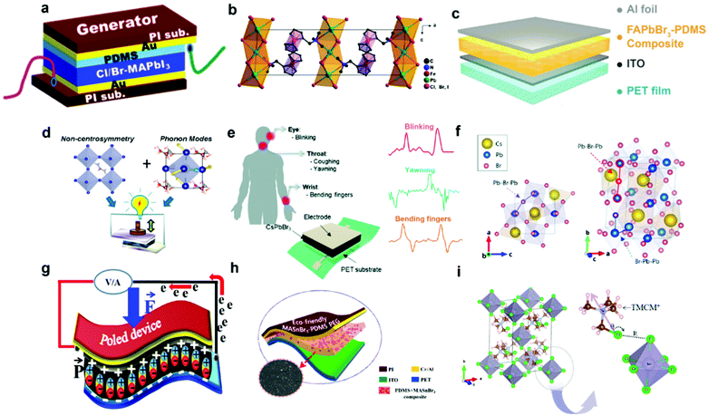
Despite the exciting progress of composition optimization for halide perovskites, an inevitable problem impeding the practical applications of HP-PENG is the intrinsic rigidity and brittleness of perovskites, causing incompatible issues toward irregular mechanical deformations and flexible applications. A prospective solution is to mix the halide perovskites with piezoelectric polymers or embed the perovskite particles into the polymer matrix to form a uniform composite film, which not only endows the HP-PENG device with remarkable flexibility and stability but also strengthens the piezoelectric output via a synergetic enhancement effect. Poly(vinylidene fluoride) (PVDF) and its copolymers are commonly used piezoelectric polymers with many different phases, including α, β, γ, δ and amorphous phases. Among these different phases, β phase is the most important polar phase that mainly contributes to the piezoelectricity, hence increasing the proportion of β phase is vital to improve the electrical properties of PVDF. Sultana et al. prepared a MAPbI3-incorporated PVDF composite film by a drop-casting method, and the composite film was sandwiched by two electrodes for fabricating the HP-PENG device (Fig. 4a).67 The boosting mechanism of the perovskite is illustrated in Fig. 4b, and the PbI3− inorganic framework possessed strong electronegative iodine atoms, so the dense negative charge would electrostatically interact with the –CH2 dipoles in the PVDF, leading to more nucleation of the electroactive phases and increased piezoelectric phase proportion. However, the piezoelectric output is quite low, with an output voltage of 1.8 V and a current of 37.5 nA, impeding the practical applications of HP-PENG. To further increase the electrical output, they adopted the electrospinning method to fabricate the MAPbBr3-PVDF nanofiber composite.68 The electrospinning technique not only endows the film with good flexibility and breathability but also realizes in situ electrical poling and mechanical stretching, benefiting the electroactive phase formation. The incorporation of halide perovskites provided the local coulomb force during the electrospinning process, which induced more charge accumulation on the film surface as shown in Fig. 4c, promoting more transformation from amorphous phases to polar β phases, thus a higher electrical output (5 V, 60 nA) can be obtained.
 |
| | Fig. 4 Device structure of the halide perovskite–piezoelectric polymer composite based PENG and the interactions between halide perovskites and polymers. (a) Device structure of the MAPbI3-PVDF composite film-based PENG. (b) The enhanced piezoelectric mechanism of the formation of the electrostatic phase in the MAPbI3-PVDF composite film. Reproduced with permission from ref. 67. Copyright 2018, American Chemical Society. (c) Schematic illustration of the function of perovskite in the polar β phase formation during the electrospinning process. Reproduced with permission from ref. 68. Copyright 2018, Elsevier. (d) The device structure of FAPbBr3–PVDF composite film-based PENG. The inset is the crystal structure of FAPbBr3. (e) Schematic representation of the vertical stress applied on FAPbBr3–PVDF composite nanogenerators. Reproduced with permission from ref. 41. Copyright 2017, Elsevier. (f) Structure illustration of (i) PVDF chain, (ii) CsPbBr3 structure, and (iii) the interaction between CsPbBr3 and PVDF. Reproduced with permission from ref. 37. Copyright 2020, Elsevier. | |
Jella et al. further optimized the piezoelectricity of HP-PENG by tuning the porosity of MAPbI3–PVDF composite films.42 As the volume ratio of perovskites increased, the pore size of the film would gradually expand in view of the fast crystallization of MAPbI3 compared to PVDF during the annealing process, resulting in the formation of the pores with various densities and sizes. When the perovskite volume ratio reaches 25%, the MAPbI3–PVDF film-based PENG demonstrated the maximum piezoelectric performance (45.6 V and 4.7 μA cm−2) with the largest dielectric constant and polarization (Pr = 0.83 μC cm−2), which was ascribed to the strong dipolar interactions between methylammonium cation and fluorine atoms of PVDF in the presence of micro-sized pores, leading to the superior interface compatibility. Further increment of MAPbI3 volume ratio will cause the agglomeration of perovskite particles, resulting in the formation of more interfacial defects and larger holes, impairing the piezoelectricity of HP-PENG.
Considering the better stability and polarization of formamidinium cation, FA-based perovskites were also utilized to fabricate the perovskite/polymer composite film for HP-PENG devices. FAPbBr3 particles were utilized to uniformly disperse in the PVDF to prepare the composite film for HP-PENG as shown in Fig. 4d.41 The piezoelectric performance (30 V, 6.2 μA cm−2) obtained from the composite film-based PENG was higher than the FAPbBr3–PDMS one (8.5 V, 3.8 μA cm−2), indicating that the PVDF layer not just served as a flexible matrix to bind the perovskite particles, but also played an important function in enhancing the piezoelectric signals. In addition, the stiff PVDF matrix also strengthened the local stress to the FAPbBr3 nanoparticles considering the high Young's modulus of PVDF. As illustrated in Fig. 4e, the nanoparticles can function as stress concentration centers when external force is applied, leading to stronger local deformations of PVDF segments and larger piezoelectric potential. Through the porosity and halogen adjustment, the FAPbBr2I–PVDF nanocomposite film was further optimized by increasing the bulk strain, providing a ∼5-fold amplification of strain-induced piezoelectric potential and ∼15-fold enhancement of output current up to 30 μA.69 All inorganic perovskite CsPbBr3 was also adopted to form a composite film with PVDF and its co-polymer series.37,70 The incorporation of CsPbBr3 into PVDF enabled the nucleation of more β phases (>90%), which originated from the bonding between the PVDF chain and CsPbBr3 surface through physisorption as displayed in Fig. 4f.37 The Pb atom of the perovskite would bond with the F atom of the PVDF, which was confirmed by the DFT calculation. The addition of perovskites endowed the film with excellent dielectric permittivity and crystallinity, generating the highest piezoelectric output voltage of 120 V and current of 35 μA.
3.4. Multiaxial ferroelectric perovskite design
Ferroelectric halide perovskites are materials with both non-centrosymmetric properties and spontaneous polarization, and this polarization can be reversed under the opposite electrical field, so they also belong to piezoelectric materials. Generally, ferroelectricity can be characterized by the ferroelectric hysteresis loop and PFM, which can determine the Pr and ferroelectric domains of materials. Multiaxial ferroelectric perovskites are highly desirable for excellent piezoelectricity because multidirectional polarization will synergistically contribute to piezoelectricity. For example, our previously mentioned TMCM-MnCl3 perovskite displayed six polar axes,48 leading to twelve different polarization directions (Fig. 5a), which has been proved by the crystallographic analysis and PFM measurements. Due to this multiaxial ferroelectric feature, the perovskite exhibited outstanding piezoelectric performance with an extremely high d33 value of 185 pm V−1. Nonetheless, designing or tuning multiaxial ferroelectric perovskites with the desired piezoelectric properties is still a huge challenge. Given this problem, Xiong's group developed the “quasi-spherical theory” based on the Curie symmetry principle,71 which can serve as a guideline for the design of multiaxial ferroelectric perovskites via the chemical design of organic cations. Briefly, a slight modification of perovskite structures by introducing some chemical groups to the spherical cations could regulate the symmetry of the perovskites, prompting the variation of dipole moment and rotational energy barrier, which could acquire the multiaxial ferroelectric phases. According to this theory, a series of multiaxial ferroelectric perovskites with high piezoresponse, such as [(CH3)3NCH2Cl]CdBr3 (d33 = 139 pm V−1)72 and [(CH3)3NCH2X]MnBr3 (d33 = ∼90 pm V−1),73 have been successfully synthesized as shown in Fig. 5b and c. Deswal et al. also designed a 1D ferroelectric perovskite of [Me3NCH2CH2OH]CdCl3 (Fig. 5d) where the hydroxyl group of the [Me3NCH2CH2OH]+ cation would coordinate with the anionic framework, which empowered the perovskite with unique zwitterionic properties and intramolecular O–H⋯Cl hydrogen bonding, leading to the effective long-range order and strong polarization.74 The [Me3NCH2CH2OH]CdCl3-based PENG displayed high electrical performance with an output voltage of 55.2 V and power density of 70.9 μW cm−2.74
 |
| | Fig. 5 Different structures of multiaxial ferroelectric halide perovskites. (a) Demonstration of twelve different polarization directions of the TMCM-MnCl3 perovskite and the corresponding experimental evidence from PFM measurements. Reproduced with permission from ref. 48. Copyright 2017, American Association for the Advancement of Science. (b) Crystal structure of [(CH3)3NCH2Cl]CdBr3 in the ferroelectric phase. The dashed lines represent the Cl-Br interactions. Reproduced with permission from ref. 72. Copyright 2018, American Chemical Society. (c) Crystal structure of [(CH3)3NCH2X]MnBr3 in the ferroelectric phase. Reproduced with permission from ref. 73. Copyright 2017, American Chemical Society. (d) Crystal structure of [Me3NCH2CH2OH]CdCl3 with the edge-sharing CdCl5O octahedra structure. The cations are coordinated alternatively above and below the perovskite framework. Reproduced with permission from ref. 74. Copyright 2020, American Chemical Society. (e) Crystal structure of (TMCM)FeBr4 and the corresponding six equivalent polarization directions. (f) Crystal structure of (TMIM)FeBr4 and the corresponding twelve equivalent polarization directions. Reproduced with permission from ref. 75. Copyright 2020, Elsevier. | |
Another scheme for designing ferroelectric perovskites is the “momentum matching theory” depending on the matching degree between the cations and anions. Specifically, in the process of phase transition, the interaction between the anion and cation would function as a rope, impeding the molecular rotation and generating the multiaxial ferroelectricity to a certain extent. Combining the “quasi-spherical theory” and “momentum matching theory” together, Zhang et al. utilized quasi-spherical FeBr4− anions to match the quasi-spherical TMFM+ cations for designing a multiaxial ferroelectric, (TMFM)FeBr4 (TMFM = trimethylfluoromethylammonium), possessing twelve different polarization directions.75 By tuning the halogen atoms in the organic cation, a series of multiaxial ferroelectric structures, such as (TMCM)FeBr4 (TMCM = trimethylchloromethylammonium) and (TMIM)FeBr4 (TMIM = trimethyliodomethylammonium), can be obtained with multidirectional polarization and good piezoelectricity, as demonstrated in Fig. 5e and f. Although these structures did not belong to perovskites, this design strategy offered an interesting direction that could excite some inspiration for the synthesis and optimization of multiaxial ferroelectric perovskites. A summary of the piezoelectric performance of different HP-PENG devices as well as the ferroelectric properties of halide perovskites are listed in Tables 1 and 2, respectively.
Table 2 Summary of the ferroelectric properties of halide perovskites
| Perovskite |
Remnant polarization (Pr, μC cm−2) |
Coercive field (Ec, kV cm−1) |
d
33 (pm V−1) |
Electrical output |
Ref. |
| MAPbI3 |
0.15 |
36 |
5.12 |
2.7 V, 0.14 μA cm−2 |
47
|
| MAPbI3–PVDF |
0.83 |
30.5 |
— |
45.6 V, 4.7 μA cm−2 |
42
|
| MAPb1−xFexBr3 |
1.6 |
18 |
17 |
7.29 V, 0.88 μA cm−2 |
35
|
| MASnI3 |
0.22 |
10 |
20.8 |
3.8 V, 0.35 μA cm−2 |
78
|
| CsPbBr3 |
0.03 |
40 |
40.3 |
16.4 V, 0.12 μA cm−2 |
14
|
| 4Cl-MAPbI3 |
0.56 |
30 |
— |
5.9 V, 0.61 μA cm−2, 1.3 μW cm−2 |
51
|
| (FMTMA)PbCl2I |
0.511 |
— |
20.6 |
4 V |
57
|
| (FMTMA)PbBr2I |
0.354 |
— |
15.4 |
— |
57
|
| (FMTMA)PbI3 |
0.005 |
— |
10.6 |
— |
57
|
| [MeNCH2CH2OH]CdCl3 |
17.1 |
1.01 |
3 |
55.2 V, 4 μA cm−2, 70.9 μW cm−2 |
74
|
| TMCM2SnCl6 |
8.7 |
0.6 |
137 |
81 V, 0.2 μA cm−2, 2.5 μW cm−2 |
32
|
| (ATHP)2PbBr2Cl2 |
5.4 |
— |
64.2 |
90 V, 6.5 μA cm−2, 1.7 μW cm−2 |
77
|
4. Halide perovskite-based triboelectric nanogenerators
4.1. Introduction
The triboelectric effect, derived from ancient Greek times, is a phenomenon where the electric charges will transfer from one substance to another one when two different materials are in contact.79 However, this effect has long been considered a negative impact on human activities and industrial manufacture as it will cause energy loss and static electricity damage. To make full use of this effect, Wang et al. developed the first TENG device to transform the irregular mechanical energy into electricity, depending on the coupling contribution of the triboelectric effect and electrostatic induction.7 Since then, numerous investigations have been conducted to optimize the structure and performance of TENG devices, and various applications have been explored from self-powered electronic devices to wearable smart sensors.80–82 To obtain the high-performance TENG, material selection is the primary concern for device fabrication. To date, tremendous materials, ranging from 2D materials to functional polymers, have been investigated to enhance the triboelectric performance.83 Among different triboelectric materials, halide perovskites, serving as emerging materials with unique optical and electronic properties, have been recognized as prospective candidates for future TENG materials. The first halide perovskite-based TENG (HP-TENG) was developed in a self-powered photodetector by combining the triboelectric and photoelectric effects.84 As shown in Fig. 6a, the HP-TENG was composed of two separate parts where the MAPbI3 film with mesoporous TiO2 particles acted as the triboelectric negative layer and the copper attached to the PET substrate played a role in both the triboelectric positive layer and electrodes. Taking this HP-TENG device as an example, the working mechanism of the vertical contact-separation mode can be explained in the following steps. Firstly, the opposite charges with equal amounts will generate at the surface of perovskites and copper when they have contacts. Then a triboelectric potential will be produced between the MAPbI3 and copper during the separation process of the two materials, so the free electrons will flow from one electrode to the other one to balance the electrical potential.
 |
| | Fig. 6 Device structures of different HP-TENGs and a summary of the triboelectric charge density of inorganic halide perovskites with different ion doping. (a) Device structure of the MAPbI3-based self-powered photodetector. Reproduced with permission from ref. 84. Copyright 2015, American Chemical Society. (b) Schematic illustration of (i) the fabrication process of CsPbBr3 thin films using a solvent-etching assisted spin-coating deposition method and (ii) CsPbBr3-based TENG structure. Reproduced with permission from ref. 86. Copyright 2020, Elsevier. (c) Device structure of Ba2+ doped CsPbBr3-based TENG. Reproduced with permission from ref. 89. Copyright 2020, Elsevier. (d) The open-circuit voltage of HP-TENG based on CsPb1−xMxBr3 (M = Mg2+, Ca2+, Sr2+ and Ba2+, x = 0–1) with different doping contents. Reproduced with permission from ref. 87. Copyright 2020, Elsevier. (e) Device structure of Cs1−xAxPbBr3 (A = Li+, Na+, K+ and Ru+, x = 0–1)-based TENG. (f) Summary of the triboelectric charge density of inorganic halide perovskites with different ion doping. Reproduced with permission from ref. 90. Copyright 2020, Royal Society of Chemistry. | |
When the separation distance is far enough, the triboelectric potential will vanish and the total charges will maintain a balanced state. By repeating the above procedures through periodically applied pressure, continuous and stable triboelectric signals will be generated. In addition, the photo-induced charges will also affect the electrical signals under the illumination state, which can function as efficient photodetectors within a broad spectrum range from UV to visible regions. Therefore, developing HP-TENG is promising for the development of multifunctional electronic devices and human–machine interface applications.
To better understand what factors affect the performance of HP-TENGs, a solid theoretical model should be constructed. In fact, Wang's group has built a model to reveal the relationship among output voltage (Vout), transferred charge (Q), and the separation displacement between two triboelectric layers (x), for both dielectric-to-dielectric and conductor-to-dielectric contact-mode TENGs.85 Their relationship is shown in the following equation:
| |  | (9) |
where
S,
x(
t),
d0 and
ρ represent the effective contact area size, the distance between the two triboelectric layers (a function of time), the effective thickness constant, and the surface charge density. For this equation,
d0 is defined as

for the dielectric-to-dielectric contact mode and

for the conductor-to-dielectric contact mode (
d1,
d2,
εr1 and
εr2 are the thickness of material 1 (dielectric or conductive material) and material 2 (dielectric material), and the dielectric constant of material 1 and material 2).
Under open-circuit (OC) conditions, there is no charge transfer (Q = 0) for both dielectric-to-dielectric contact and conductor-to-dielectric contact modes, so Voc is given by:
| |  | (10) |
Under short-circuit (SC) conditions (V = 0), the transferred charges and current can be described as follows:
| |  | (11) |
| |  | (12) |
From these equations, it is known that Voc is only related to surface charge density and the relative distance between two triboelectric layers, while Qsc and Isc are also affected by the effective contact area, dielectric property, and the thickness of materials. According to this theoretical model, increasing the surface charge density is vital to improve the triboelectric output, including the voltage, current, and transferred charge. Hence, charge trapping capacity optimization and photo-induced charge contribution are promising strategies to enhance the triboelectric performance of HP-TENGs. Another optimization method to increase the triboelectric output is to tune the thickness and dielectricity of halide perovskites, which can improve the output current and transferred charge. Hence, the composition optimization can play a crucial function in improving the dielectric constant of halide perovskites. Based on the theoretical analysis and recent experimental progress, the different optimization strategies for enhancing the electrical performance of HP-TENGs will be introduced in this section.
4.2. Composition optimization of halide perovskites
Similar to the strategy of HP-PENG, composition optimization is also crucial to the triboelectric performance viewing the improved dielectricity and morphology.86–88 Du et al. systematically investigated the halide ion doping effects on the triboelectric behaviors of inorganic CsPbX3 (X = Cl, Br, I) perovskites via a solvent-etching assisted spin-coating deposition method (Fig. 6b).86 In general, the HP-TENG performance was mainly determined by the transferred charge between two triboelectric layers, relying on the charge density concerned with the surface morphology as well as the material polarization associated with charge affinity. By doping the Cl− and I− ions to the CsPbBr3 perovskite, the polarity and [PbBr6]4− octahedral structure were distinctly regulated, promoting the surface morphology and dielectric permittivity improvement. Compared with the Cl-doping one, I-containing perovskite TENG exhibited higher electric output because of the lattice expansion. After precise ratio optimization, the best performance with an output voltage of 192 V, current of 16.7 μA and power density of 1.2 W m−2 can be obtained.
Metal ion doping is also essential to surface morphology and dielectricity optimization. As illustrated in Fig. 6c, Wang et al. established a HP-TENG device using a Ba2+ doped CsPbBr3 film and PVDF as triboelectric layers.89 With the increment of Ba2+ concentration, the grain size would gradually decrease as a result of the suppressed perovskite formation energy and fast nucleation originating from lattice expansion, causing the enlarged electron density and the lattice modulation of octahedra structure. The density of grain boundaries greatly influenced the space charge distribution of the perovskites because the grain boundaries would serve as charge traps that capture and store the surface charge, affecting the space charge polarization and triboelectric performance. In addition, the content of Ba2+ also influenced the dielectricity, work function, binding energy and surface potentials of perovskites, which further manipulated the TENG output. Through the doped Ba2+ concentration tuning, the maximum output voltage and power density can reach 220 V and 3.07 W m−2, respectively. Following this work, a series of metal cations, such as Mg2+, Ca2+, Sr2+ and Ba2+, were adopted to partially replace the Pb2+ in the CsPbBr3 perovskite.87 The detailed optimization results were summarized in Fig. 6d, and the Ba2+ doped CsPb0.91Ba0.09Br3 displayed the best electrical performance (222 V, 3.48 μA cm−2), which was attributed to its lowest binding energy and work function, indicating the Ba2+ doped perovskites could more easily lose the electrons during the contact-separation process and generate more triboelectric negative charges. Similarly, the Cs+ site in the inorganic halide perovskite could also be partially replaced by other monovalent cations to tune the dielectricity, surface potential, work function and polarity of perovskite following the same mechanism. Based on this idea, the authors also designed a series of inorganic Cs1−xAxPbBr3 (A = Li+, Na+, K+ and Ru+, x = 0–1) perovskites to modify their composition ratio for improving the triboelectric performance.90 The device structure and the corresponding electrical properties with different doping contents are summarized in Fig. 6e and f. Thanks to these state-of-the-art studies, halide perovskites have been proved to have an excellent electrical performance for TENG applications, which dramatically expand the range of triboelectric materials, bringing new chances for the development of multifunctional and self-powered electronic devices.
To better understand the intrinsic nature of HP-TENGs, it is significant to determine the triboelectric charge density of halide perovskites in the triboelectric series. In 2019, Wang's group proposed a standard method to quantitatively measure the triboelectric charge density via a liquid metal contact process in a well-controlled condition, which established a normalized method to reflect the intrinsic nature of triboelectric materials for gaining or losing electrons, providing the guidance for material selection in fabricating TENG devices.83 To extend the scope of material selection and enrich the existing triboelectric series, Wang et al. conducted some pioneering research to compare the halide perovskite CsPbBr3 and its alkali/alkaline earth ion-doped derivatives (Cs1−xAxPb1−yMyBr3, A = Li+, Na+, K+, and Ru+, M = Mg2+, Ca2+, Sr2+, and Ba2+, x/y = 0–1) with the conventional triboelectric materials (nylon, polyimide (PI), PET, polycarbonate (PC), polyethylene (PE), PDMS, PVDF, and polytetrafluoroethylene (PTFE)).87,90 It was found that all these perovskites would distribute between PC and PE in the triboelectric series from the electrical tests and qualitative triboelectric charge density measurements (Fig. 7). By substituting the Cs-site and Pb-site with different alkali metal ions and alkaline earth ions, the energy level, crystallinity, dielectric properties, work function and electron binding energy of halide perovskites were also changed, which further affected their triboelectric output, realizing the fine-tuning of triboelectric behaviors in the triboelectric series. These studies not only revealed the triboelectric properties of halide perovskites in triboelectric series but also proposed a strategy for the new material design of TENGs.
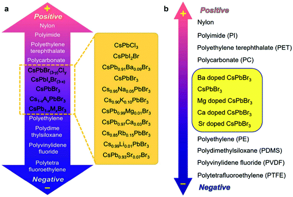 |
| | Fig. 7 Triboelectric series of CsPbBr3 perovskite and its Cs-site and Pb-site substituted compounds. Qualitative triboelectric series of the (a) pristine CsPbBr3, Cs1−xAxPbBr3 and (b) CsPb1−xMxBr3 perovskites. Reproduced with permission from ref. 87 and 90. Copyright 2020 from Elsevier and Copyright 2020 from Royal Society of Chemistry. | |
4.3. Charge trapping capacity optimization
Increasing the charge density and storing the charge of triboelectric materials are also effective strategies that can improve the electrical output of HP-TENG.91–94 The maximum surface charge density is restricted by the air breakdown effect,95 which can be optimized by diminishing the thickness of the triboelectric layer, regulating the environmental humidity, reducing the testing pressure and raising the capacitance of the circuit,96,97 while the charge trapping and storing capacity can be controlled by modifying the structure or inducing the intermediate layer to the triboelectric materials.98 The concept of incorporating the intermediate layers into the triboelectric layers was firstly introduced in 2016, functioning as an efficient strategy to reinforce the charge trapping capacity and broaden the charge decay time; thus the triboelectric output was greatly enhanced.99,100 From this point of view, Wang et al. embedded the noble metal particles (Au, Ag, Pt) into the inorganic CsPbBr3 perovskite film to introduce the Schottky junction, which increased the local electrical field and electron transfer rate, promoting the charge accumulation process at the bottom electrode.101 Hence, the total power output of TENG was enormously improved. The device structure and the corresponding enhancing mechanism are shown in Fig. 8a and b. Specifically, an equal number of positive and negative charges were generated at the surface of the CsPbBr3–metal composite and PVDF film during the contact process. Then the charge density of the CsPbBr3 surface would gradually reduce because of the electron drift/diffusion process and screening effect, leading to the decreased potential difference between the two electrodes. Owing to the incorporation of noble metal nanoparticles, plentiful Schottky junctions were induced in the interfaces between metal and perovskites, resulting in the continuous electron transfer process. Under the equilibrium state, many Helmholtz double layers were formed at the perovskite/metal interface as shown in Fig. 8b, thus the CsPbBr3 layer would be more positively charged with a higher surface charge density. Moreover, the electron drift/diffusion process and screening effect were also alleviated in the presence of the space positive charge area, which was also beneficial to the charge trapping capacity of the perovskite. After the work function adjustment of different noble metals, the optimized HP-TENG device can achieve the best electrical performance with an output voltage of 240 V and a short-circuit current density of 4.13 μA cm−2.101 Xie et al. also designed a bulk Pt/CsPbBr3-based HP-TENG following the same device structure and mechanism.102 Briefly, the space between perovskite and Pt was considered as capacitors (Fig. 8c), which were expected to enhance the total capacity of the bulk film, boosting the charge trapping capacity and surface charge density. Through the optimization of Pt dosage (0.5% Pt dosage), the maximum output voltage and current density can raise to 273 V and 30.3 μA cm−2. Du et al. further induced the Co(OH)(CO3)0.5 to form a Co(OH)(CO3)0.5/Pt/CsPbIBr2 multilayer nanoarray structure with a rhombus shape for the HP-TENG (Fig. 8d).103 Assisted by the structure improvement, the contact surface area was significantly enlarged and the triboelectric charge dynamic behaviors were well controlled via interfacial polarization between Pt/perovskite and Co(OH)(CO3)0.5, which extended the in-depth distribution of triboelectric charges and inhibited the charge drift and diffusion process of the perovskite layer, generating a high power density up to 2.04 W m−2.
 |
| | Fig. 8 Charge trapping optimization and photoinduced electrical enhancement of different HP-TENGs. (a) Device structure of CsPbBr3–Au composite-based TENG. (b) The working mechanism of triboelectric enhancement in the metal/perovskite Schottky junction. Reproduced with permission from ref. 101. Copyright 2020, Elsevier. (c) Schematic illustration of the nanocapacitor structures in the Pt/CsPbBr3 film. Reproduced with permission from ref. 102. Copyright 2020, Royal Society of Chemistry. (d) Device structure of rhombus Co(OH)(CO3)0.5/Pt/CsPbIBr2-based TENG and the corresponding crystal structure of CsPbIBr2. Reproduced with permission from ref. 103. Copyright 2020, Elsevier. (e) Device structure of MAPbI3-based TENG under the illumination state and the surface potential of the MAPbI3 perovskite at four different states (the initial state under dark conditions, the state after 5 minute-rubbing under dark conditions, the state after rubbing under the illumination state, and the stable state after the charge decay process). Reproduced with permission from ref. 104. Copyright 2016, Royal Society of Chemistry. (f) Device structure of PTFE - pentacene/perovskite/TiO2 TENG and the corresponding cross-sectional SEM image. (g) The working mechanism of the HP-TENG device under the illumination. Reproduced with permission from ref. 105. Copyright 2019, Springer Nature. (h) Device structure of CsPbBr3/PC TENG. (i) Energy level illustration of the HP-TENG under friction-illumination working conditions. Reproduced with permission from ref. 15. Copyright 2021, John Wiley and Sons. | |
4.4. Photoinduced electrical output enhancement
Although many efforts have been conducted for the composition and charge trapping capacity optimization of HP-TENG, the unique photoelectric performance of perovskites should not be ignored as well. Su et al. presented the first photo-assisted enhancement of TENG based on a MAPbI3 perovskite, as demonstrated in Fig. 8e.104 In the device structure, the MAPbI3/TiO2 and PTFE film served as triboelectric positive and negative layers, which were attached to the FTO and copper electrode, respectively. The mesostructured TiO2 layer played a crucial function in the electron transfer. Under the illumination condition, many electron–hole pairs were produced at the surface of perovskites. Due to the presence of the TiO2 scaffold, the generated electrons were rapidly transported away from the perovskite layer, leaving a large number of holes at the surface. These holes, combined with the triboelectric positive charges, synergistically contributed to the electrical output, enabling the output voltage and current density to rise from 15.3 V and 72.5 nA cm−2 under dark conditions to 17 V and 95 nA cm−2 under illumination conditions.104 Despite the improvement in electrical output, the increment was still modest. Based on this work, the device was further optimized by adding another ultrathin pentacene layer, providing a chance for both electron and hole transport, as illustrated in Fig. 8f.105 Briefly, under the dark environment, triboelectric positive and negative charges separately accumulated on the surface of the pentacene and PTFE during the mechanical contact-separation process. Once the light was shed on the device, lots of electron–hole pairs were generated in the perovskites. As efficient hole and electron transporting layers, the pentacene and TiO2 would quickly trap the photoinduced holes and electrons, resulting in a larger surface charge density, which was shown in Fig. 8g. Hence the triboelectric output was enhanced from 14.64 V and 0.87 μA cm−2 (dark) to 22.80 V and 1.31 μA cm−2 (light). Apart from the regulation of hole and electron transport layers, tuning the triboelectric layer and constructing the Schottky junction are also good strategies to strengthen the photoinduced carrier extracting efficiency, thus increasing the triboelectric output.15,106 As shown in Fig. 8h, Guo et al. developed a CsPbBr3-based TENG, where the triboelectric negative layer was composed of a PDMS-multiwall carbon nanotubes (MWCNTs) composite (PC) film acting as both the triboelectric negative layer and hole-extraction layer.15 Through the MWCNT loading optimization, the surface charge density of the PC film was greatly improved, prompting the triboelectric performance. Typically, electron-hole carriers were generated at the surface of the CsPbBr3 perovskite under the illumination conditions, but they were hard to extract by the pure PDMS due to the insulating features, thus most carriers were randomly scattered or recombined together. In comparison, the work function difference between the PC film and perovskite can be reduced via MWCNT tuning, generating a built-in electrical potential owing to the Fermi levels alignment as depicted in Fig. 8i, which diminished the triboelectric voltage but facilitated the carrier separation and charge transfer at the interfaces, advancing the current density and power density. Under the illumination state, the current density was raised from 0.735 μA cm−2 to 400 μA cm−2, which was enhanced more than 500 times.15 A summary of the device structure and triboelectric performance of different HP-TENGs is listed in Table 3.
Table 3 Summary of halide perovskite-based TENG devices
| Perovskite |
Device structure |
Device active size |
Voltage |
Current density |
Power density |
Charge transfer |
Ref. |
| MAPbI3 film |
PET/Cu(+)-(−)MAPbI3–TiO2 NPs/TiO2/FTO |
2 × 2 cm2 |
8 V (no light) |
— |
— |
— |
84
|
| 5 V (light) |
| MAPbI3 film |
Cu/PTFE(−)-(+)MAPbI3–TiO2 NPs/TiO2/FTO |
2 × 2 cm2 |
15.3 V (no light) |
72.5 nA cm−2 (no light) |
— |
5.7 nC (no light) |
104
|
| 17 V (light) |
95 nA cm−2 (light) |
|
6.2 nC (light) |
| MAPbClxI3−x film |
Al/PTFE(−)-(+)pentacene/MAPbCl0.3I2.7/TiO2/FTO |
∼0.7 cm2 |
14.64 V (no light) |
0.87 μA cm−2 (no light) |
10.3 μW cm−2 (no light) |
5.05 nC (no light) |
105
|
| 22.80 V (light) |
1.31 μA cm−2 (light) |
17.9 μW cm−2 (light) |
7.99 nC (light) |
| (MA)0.5(FA)0.5Pb0.5Sn0.5I3 film |
Al(−)-(+) (MA)0.5(FA)0.5Pb0.5Sn0.5I3/ITO/PET (Schottky junction) |
0.0003 cm2 |
∼0.7 V (No light) |
−0.55 μA (no light) |
— |
— |
106
|
| −1.80 μA (light) |
| CsPb1−xBaxBr3 film |
Ag/PVDF(−)-(+) CsPb0.91Ba0.09Br3/FTO/Glass |
8.1 cm2 |
220 V |
2.28 μA cm−2 |
3.07 W m−2 |
70 nC |
103
|
| CsPbX3 film (X = Cl, Br, I) |
Ag/PVDF(−)-(+)CsPbBr2.6I0.4/FTO/Glass |
3 × 3 cm2 |
192 V |
1.86 μA cm−2 |
1.20 W m−2 |
79.5 nC |
86
|
| CsPbBr3 film |
Al/PVDF(−)-(+)CsPbBr3/Au NPs/FTO/Glass |
2 × 3 cm2 |
240 V |
4.13 μA cm−2 |
3.31 W m−2 |
— |
101
|
| Co(OH)(CO3)0.5/Pt/CsPbBr2I film |
Ag/PVDF(−)-(+)CsPbBr2I/Pt/Co(OH)(CO3)0.5/FTO/Glass |
3 × 3 cm2 |
243 V |
3.10 μA cm−2 |
2.04 W m−2 |
86 nC |
103
|
| CsPb1−xMxBr3 film (M = Mg2+, Ca2+, Sr2+, Ba2+, x = 0–1) |
Ag/PVDF(−)-(+) CsPb0.91Ba0.09Br3/FTO/Glass |
8.1 cm2 |
222 V CsPb0.91Ba0.09Br3 |
3.48 μA cm−2 Ba2+ doping |
— |
88 nC Ba2+ doping |
87
|
| 142 V CsPb0.99Mg0.01Br3 |
2.32 μA cm−2 Mg2+ doping |
|
60 nC Mg2+ doping |
|
| 138 V CsPb0.97Ca0.03Br3 |
1.99 μA cm−2 Ca2+ doping |
|
58 nC Ca2+ doping |
|
| 127 V CsPb0.93Sr0.07Br3 |
1.73 μA cm−2 Sr2+ doping |
|
53 nC Sr2+ doping |
|
| ∼180 V(CsPbBr3) |
∼3.09 μA cm−2 (CsPbBr3) |
|
∼73 nC (CsPbBr3) |
|
| CsPbBr3 film |
Al/PVDF(−)-(+)CsPbBr3-0.5% Pt NPs/FTO/Glass |
3 × 3 cm2 |
273 V |
30.3 μA cm−2 |
1.295 W m−2 |
101 nC |
102
|
| CsPbX3 film (X = Cl, Br, I) |
Al/PVDF(−)-(+)CsPbCl3/FTO/Glass |
7.5 cm2 |
257 V |
3.72 μA cm−2 |
3.04 W m−2 |
79.8 nC |
87
|
| Cs1−xAxPbBr3 film (A = Li+, Na+, K+, and Ru+, x = 0–1) |
Al/PVDF(−)-(+)Cs1−xAxPbBr3/FTO/glass |
8.1 cm2 |
128 V Cs0.99–Li0.01PbBr3 |
2.11 μA cm−2 Li+ doping |
— |
55 nC Li+ doping |
90
|
|
|
135 V Cs0.85–Rb0.15PbBr3 |
2.22 μA cm−2 Rb+ doping |
|
57 nC Rb+ doping |
|
|
|
152 V Cs0.90–K0.10PbBr3 |
2.51 μA cm−2 K+ doping |
|
|
|
|
|
158 V Cs0.95–Na0.05PbBr3 |
2.52 μA cm−2 Na+ doping |
|
66 nC Na+ doping |
|
|
|
182 V(CsPbBr3) |
2.84 μA cm−2 (CsPbBr3) |
|
73 nC (CsPbBr3) |
|
| CsPbCl3 film |
Ag/PVDF(−)-(+)CsPbCl3/FTO/Glass |
7.5 cm2 |
258 V |
4 μA cm−2 |
3.06 W m−2 |
79.9 nC |
88
|
| CsPbBr3 film |
Ag/MWCNT(12 wt%)-PDMS(−)-(+)CsPbBr3/FTO/Glass |
7.5 cm2 |
7.85 V (no light) |
0.735 μA cm−2 (no light) |
6.66 W m−2 (no light) |
13.4 nC (no light) |
15
|
| ∼1 V (light) |
∼400 μA cm−2 (light) |
8.24 W m−2 (light) |
161 nC (light) |
|
| Cs3Bi2Br9–PVDF-HFP nanofiber composite |
Ag-SEBS/Cs3Bi2Br9–PVDF-HFP(−)-(+)Al |
3 × 4 cm2 |
400 V |
1.63 μA cm−2 |
2.34 W m−2 |
30 nC |
94
|
5. Conclusions and outlooks
In this review, the state-of-the-art research progress as well as the design and optimization strategies of halide perovskite-based mechanical harvesters, including PENG and TENG devices are summarized. For HP-PENGs, composition regulation, a mixture with piezoelectric polymers, as well as multiaxial ferroelectric perovskite design are advantageous methods that cannot only increase the polarization, surface morphology and piezoelectricity of the devices, but also endow the perovskites with improved flexibility and mechanical properties. As for HP-TENGs, composition optimization, charge trapping capacity improvement, and photoinduced electrical enhancement are efficient approaches endowing the device with outstanding dielectricity, charge storage and photoelectricity, boosting the surface charge density and triboelectric output.
Despite the promising progress, some aspects related to the intrinsic properties of halide perovskites need to be considered for the more far-reaching development. First of all, the intrinsic rigidity and brittleness of perovskites will severely limit the applications of flexible and wearable electronics. Although PENG devices can partially solve this problem by mixing the perovskites with soft polymers, few studies have been conducted to deal with the challenge in TENG applications. Secondly, the toxicity of lead elements is another issue restricting the broader applications of halide perovskite-based energy harvesters given their potential safety risks to human health and the ecological environment. Some lead-free halide perovskites, such as tin-based perovskites, have shown comparable performance similar to the Pb-based ones, but the poor stability of the Sn element causes another problem for practical applications. Thus, developing stable and high-performance lead-free perovskites is also significant to the future development of halide perovskite-based energy harvesters. Next, the design principle of high-performance piezoelectric halide perovskites is still not clear. For example, the ferroelectric perovskites with high remanent polarization are generally endowed with high piezoelectricity, but the actual piezoelectricity and remanent polarization do not show a clear functional relationship as shown in Table 2, possibly owing to the influence of other factors, such as the surface morphology, dielectricity and electronic properties of perovskites. Therefore, constructing a complete theory that serves as a framework for the design of piezoelectric perovskites with high performance is crucial to the profound development in this field. Lastly, the challenges of low moisture and thermal stability of perovskites also constrain their practical long-term applications, posing another obstacle in halide perovskite-based energy devices.
In spite of these challenges and issues, numerous opportunities and prospective directions still exist in halide perovskite-based mechanical energy harvesters, especially in the applications of versatile energy conversion and harvesting, direct current (DC) TENGs, and multifunctional device design. For HP-PENGs, the emerging ferroelectric 2D and 3D halide perovskites not only provide an effective platform for designing high-performance piezoelectric materials via the induction of an organic cation moiety with strong and multiaxial polarizations, but also endow the new PENG devices with some unique functions, including pyroelectric,107 flexoelectric,12 photovoltaic,108 and semiconducting properties. By combining or coupling these different functions into one device, a series of promising properties, such as the piezo-phototronic effect (a coupling effect of piezoelectricity, photoexcitation and semiconducting features)109 and photoflexoelectric effect (a coupling effect of flexoelectricity, light absorption and semiconducting features),110 can be obtained, enabling the energy harvesting from various energy inputs (electromechanical, pyroelectric, and photovoltaic energy). For HP-TENGs, the unique semiconducting properties, tunable energy levels and bandgap, excellent light absorption and photovoltaic properties of halide perovskites also open a fresh avenue for the future development of TENG devices. For example, some pioneering work has been conducted to construct halide perovskite-based Schottky and heterojunction junctions for the design of direct current (DC) TENGs,106,111 which can directly charge electronic devices without the requirement of rectifiers. Further investigation on their tribovoltaic or tribo-photovoltaic effect112 also indicated that the electrical output of these DC TENGs can be greatly enhanced under the illumination, exhibiting their huge potential in self-powered photodetectors and photo-enhanced mechanical energy harvesting. Finally, many excellent properties of perovskites, such as the photoelectric, thermoelectric, ionic and luminous properties, are rarely explored in combination with the function of energy harvesting, which is the unique superiority of the perovskite materials. The coupling effect among these different functions should be further investigated and more efforts should be focused on the halide perovskite-based all-in-one platform design for the integration of energy harvesting and multiple electronic functions. For example, based on the triboelectric, piezoelectric, flexoelectric, pyroelectric, photovoltaic, or a combination of the above effects, halide perovskite-based energy harvesters can simultaneously collect different forms of energy, including the biomechanical, thermal and solar energy, from the human motion and ambient environment. Subsequently, they can convert the energy into electricity that further powers different electronic devices, such as LEDs, field-effect transistors, memory devices, smart windows and sensors, realizing a halide perovskite-based hybrid energy system that achieves both power supply and multifunctional device integration. Hence developing halide perovskite-based self-powered multifunctional electronic devices is a promising field for the future applications of artificial intelligence, the internet of things, smart sensors and wearable electronics.
Conflicts of interest
There are no conflicts to declare.
Acknowledgements
This work was supported by the Ministry of Education (MOE) Singapore, AcRF Tier 1 grant no. RT15/20 and NGF-2020-09-012. F. J. acknowledges the research scholarship awarded by the Institute of Flexible Electronics Technology of Tsinghua, Zhejiang (IFET-THU), Nanyang Technological University (NTU), and Qiantang Science and Technology Innovation Center, China (QSTIC).
Notes and references
- W.-G. Kim, D.-W. Kim, I.-W. Tcho, J.-K. Kim, M.-S. Kim and Y.-K. Choi, ACS Nano, 2021, 15, 258–287 CrossRef CAS PubMed.
- H. Wang, M. Han, Y. Song and H. Zhang, Nano Energy, 2021, 81, 105627 CrossRef CAS.
- S. M. A. Z. Shawon, A. X. Sun, V. S. Vega, B. D. Chowdhury, P. Tran, Z. D. Carballo, J. A. Tolentino, J. Li, M. S. Rafaqut, S. Danti and M. J. Uddin, Nano Energy, 2021, 82, 105691 CrossRef CAS.
- Y. Zhang, H. Kim, Q. Wang, W. Jo, A. I. Kingon, S.-H. Kim and C. K. Jeong, Nanoscale Adv., 2020, 2, 3131–3149 RSC.
- C. K. Jeong, MRS Commun., 2020, 10, 365–378 CrossRef CAS.
- Z. L. Wang and J. Song, Science, 2006, 312, 242–246 CrossRef CAS PubMed.
- F.-R. Fan, Z.-Q. Tian and Z. Lin Wang, Nano Energy, 2012, 1, 328–334 CrossRef CAS.
- J. J. Yoo, G. Seo, M. R. Chua, T. G. Park, Y. Lu, F. Rotermund, Y.-K. Kim, C. S. Moon, N. J. Jeon, J.-P. Correa-Baena, V. Bulović, S. S. Shin, M. G. Bawendi and J. Seo, Nature, 2021, 590, 587–593 CrossRef CAS PubMed.
- G. Pacchioni, Nat. Rev. Mater., 2021, 6, 108 CrossRef CAS.
- H. Jing, R. Peng, R.-M. Ma, J. He, Y. Zhou, Z. Yang, C.-Y. Li, Y. Liu, X. Guo, Y. Zhu, D. Wang, J. Su, C. Sun, W. Bao and M. Wang, Nano Lett., 2020, 20, 7144–7151 CrossRef CAS PubMed.
- K. Kobbekaduwa, S. Shrestha, P. Adhikari, E. Liu, L. Coleman, J. Zhang, Y. Shi, Y. Zhou, Y. Bekenstein, F. Yan, A. M. Rao, H. Tsai, M. C. Beard, W. Nie and J. Gao, Nat. Commun., 2021, 12, 1636 CrossRef CAS PubMed.
- D. Liu, D. Luo, A. N. Iqbal, K. W. P. Orr, T. A. S. Doherty, Z.-H. Lu, S. D. Stranks and W. Zhang, Nat. Mater., 2021, 20, 1337–1346 CrossRef CAS PubMed.
- C. Ashworth, Nat. Rev. Mater., 2021, 6, 293 CrossRef CAS.
- D. B. Kim, K. H. Park and Y. S. Cho, Energy Environ. Sci., 2020, 13, 2077–2086 RSC.
- Q. Guo, X. Yang, Y. Wang, W. Xu, J. Duan and Q. Tang, Adv. Funct. Mater., 2021, 31, 2101348 CrossRef CAS.
- H. Park, C. Ha and J.-H. Lee, J. Mater. Chem. A, 2020, 8, 24353–24367 RSC.
- V. Jella, S. Ippili, J.-H. Eom, S. V. N. Pammi, J.-S. Jung, V.-D. Tran, V. H. Nguyen, A. Kirakosyan, S. Yun, D. Kim, M. R. Sihn, J. Choi, Y.-J. Kim, H.-J. Kim and S.-G. Yoon, Nano Energy, 2019, 57, 74–93 CrossRef CAS.
- R. Ding, X. Zhang and X. W. Sun, Adv. Funct. Mater., 2017, 27, 1702207 CrossRef.
-
H.-R. Wenk and A. Bulakh, Minerals: their constitution and origin, Cambridge University Press, 2016 Search PubMed.
- L. Mao, C. C. Stoumpos and M. G. Kanatzidis, J. Am. Chem. Soc., 2019, 141, 1171–1190 CrossRef CAS PubMed.
- G. Kieslich, S. Sun and A. K. Cheetham, Chem. Sci., 2014, 5, 4712–4715 RSC.
- Q. Van, Le, H. W. Jang and S. Y. Kim, Small Methods, 2018, 2, 1700419 CrossRef.
- Z. Li, M. Yang, J.-S. Park, S.-H. Wei, J. J. Berry and K. Zhu, Chem. Mater., 2016, 28, 284–292 CrossRef CAS.
- K. Leng, W. Fu, Y. Liu, M. Chhowalla and K. P. Loh, Nat. Rev. Mater., 2020, 5, 482–500 CrossRef CAS.
- E. Shi, Y. Gao, B. P. Finkenauer, Akriti, A. H. Coffey and L. Dou, Chem. Soc. Rev., 2018, 47, 6046–6072 RSC.
- E. S. Vasileiadou, B. Wang, I. Spanopoulos, I. Hadar, A. Navrotsky and M. G. Kanatzidis, J. Am. Chem. Soc., 2021, 143, 2523–2536 CrossRef CAS PubMed.
- P. Fu, Y. Liu, S. Yu, H. Yin, B. Yang, S. Ahmad, X. Guo and C. Li, Nano Energy, 2021, 88, 106249 CrossRef CAS.
- J. Qiu, Y. Xia, Y. Zheng, W. Hui, H. Gu, W. Yuan, H. Yu, L. Chao, T. Niu, Y. Yang, X. Gao, Y. Chen and W. Huang, ACS Energy Lett., 2019, 4, 1513–1520 CrossRef CAS.
- P. Liu, N. Han, W. Wang, R. Ran, W. Zhou and Z. Shao, Adv. Mater., 2021, 33, 2002582 CrossRef CAS PubMed.
- L. Mao, W. Ke, L. Pedesseau, Y. Wu, C. Katan, J. Even, M. R. Wasielewski, C. C. Stoumpos and M. G. Kanatzidis, J. Am. Chem. Soc., 2018, 140, 3775–3783 CrossRef CAS PubMed.
- Y. Wu, J. Qu, W. A. Daoud, L. Wang and T. Qi, J. Mater. Chem. A, 2019, 7, 13347–13355 RSC.
- G. Huang, A. A. Khan, M. M. Rana, C. Xu, S. Xu, R. Saritas, S. Zhang, E. Abdel-Rahmand, P. Turban, S. Ababou-Girard, C. Wang and D. Ban, ACS Energy Lett., 2021, 6, 16–23 CrossRef CAS.
- Z. Yang, S. Zhou, J. Zu and D. Inman, Joule, 2018, 2, 642–697 CrossRef CAS.
- P. Adhikary, S. Garain and D. Mandal, Phys. Chem. Chem. Phys., 2015, 17, 7275–7281 RSC.
- S. Ippili, V. Jella, J. Kim, S. Hong and S.-G. Yoon, Nano Energy, 2018, 49, 247–256 CrossRef CAS.
- S. Ippili, V. Jella, J.-H. Eom, J. Kim, S. Hong, J.-S. Choi, V.-D. Tran, N. Van Hieu, Y.-J. Kim and H.-J. Kim, Nano Energy, 2019, 57, 911–923 CrossRef CAS.
- S. Mondal, T. Paul, S. Maiti, B. K. Das and K. K. Chattopadhyay, Nano Energy, 2020, 74, 104870 CrossRef CAS.
- H. Fu and R. E. Cohen, Nature, 2000, 403, 281–283 CrossRef CAS PubMed.
- Y. Yan, J. E. Zhou, D. Maurya, Y. U. Wang and S. Priya, Nat. Commun., 2016, 7, 1–10 Search PubMed.
- F. Li, D. Lin, Z. Chen, Z. Cheng, J. Wang, C. Li, Z. Xu, Q. Huang, X. Liao and L.-Q. Chen, Nat. Mater., 2018, 17, 349–354 CrossRef CAS PubMed.
- R. Ding, X. Zhang, G. Chen, H. Wang, R. Kishor, J. Xiao, F. Gao, K. Zeng, X. Chen, X. W. Sun and Y. Zheng, Nano Energy, 2017, 37, 126–135 CrossRef CAS.
- V. Jella, S. Ippili, J.-H. Eom, J. Choi and S.-G. Yoon, Nano Energy, 2018, 53, 46–56 CrossRef CAS.
- X. Wang, W.-Z. Song, M.-H. You, J. Zhang, M. Yu, Z. Fan, S. Ramakrishna and Y.-Z. Long, ACS Nano, 2018, 12, 8588–8596 CrossRef CAS PubMed.
- M.-L. Seol, J.-M. Choi, J.-Y. Kim, J.-H. Ahn, D.-I. Moon and Y.-K. Choi, Nano Energy, 2013, 2, 1142–1148 CrossRef CAS.
- L. Gu, J. Liu, N. Cui, Q. Xu, T. Du, L. Zhang, Z. Wang, C. Long and Y. Qin, Nat. Commun., 2020, 11, 1030 CrossRef CAS PubMed.
- W.-Q. Liao, D. Zhao, Y.-Y. Tang, Y. Zhang, P.-F. Li, P.-P. Shi, X.-G. Chen, Y.-M. You and R.-G. Xiong, Science, 2019, 363, 1206–1210 CrossRef CAS PubMed.
- Y.-J. Kim, T.-V. Dang, H.-J. Choi, B.-J. Park, J.-H. Eom, H.-A. Song, D. Seol, Y. Kim, S.-H. Shin, J. Nah and S.-G. Yoon, J. Mater. Chem. A, 2016, 4, 756–763 RSC.
- Y.-M. You, W.-Q. Liao, D. Zhao, H.-Y. Ye, Y. Zhang, Q. Zhou, X. Niu, J. Wang, P.-F. Li, D.-W. Fu, Z. Wang, S. Gao, K. Yang, J.-M. Liu, J. Li, Y. Yan and R.-G. Xiong, Science, 2017, 357, 306–309 CrossRef CAS PubMed.
- Z. L. Wang, Mater. Today, 2017, 20, 74–82 CrossRef.
- Z. L. Wang, Nano Energy, 2020, 68, 104272 CrossRef CAS.
- V. Jella, S. Ippili and S.-G. Yoon, ACS Appl. Electron. Mater., 2020, 2, 2579–2590 CrossRef CAS.
- R. Pandey, G. Sb, S. Grover, S. K. Singh, A. Kadam, S. Ogale, U. V. Waghmare, V. R. Rao and D. Kabra, ACS Energy Lett., 2019, 4, 1004–1011 CrossRef CAS.
- V. Jella, S. Ippili, J.-H. Eom, Y.-J. Kim, H.-J. Kim and S.-G. Yoon, Nano Energy, 2018, 52, 11–21 CrossRef CAS.
- J. M. Frost, K. T. Butler, F. Brivio, C. H. Hendon, M. van Schilfgaarde and A. Walsh, Nano Lett., 2014, 14, 2584–2590 CrossRef CAS PubMed.
- J. Ma and L.-W. Wang, Nano Lett., 2015, 15, 248–253 CrossRef CAS PubMed.
- Y. Kutes, L. Ye, Y. Zhou, S. Pang, B. D. Huey and N. P. Padture, J. Phys. Chem. Lett., 2014, 5, 3335–3339 CrossRef CAS PubMed.
- Z.-X. Zhang, H.-Y. Zhang, W. Zhang, X.-G. Chen, H. Wang and R.-G. Xiong, J. Am. Chem. Soc., 2020, 142, 17787–17794 CrossRef CAS PubMed.
- R. Ding, H. Liu, X. Zhang, J. Xiao, R. Kishor, H. Sun, B. Zhu, G. Chen, F. Gao, X. Feng, J. Chen, X. Chen, X. Sun and Y. Zheng, Adv. Funct. Mater., 2016, 26, 7708–7716 CrossRef CAS.
- C. C. Stoumpos, C. D. Malliakas and M. G. Kanatzidis, Inorg. Chem., 2013, 52, 9019–9038 CrossRef CAS PubMed.
- T. M. Koh, T. Krishnamoorthy, N. Yantara, C. Shi, W. L. Leong, P. P. Boix, A. C. Grimsdale, S. G. Mhaisalkar and N. Mathews, J. Mater. Chem. A, 2015, 3, 14996–15000 RSC.
- L. Theofylaktos, K. O. Kosmatos, E. Giannakaki, H. Kourti, D. Deligiannis, M. Konstantakou and T. Stergiopoulos, Dalton Trans., 2019, 48, 9516–9537 RSC.
- Y. Yuan, X.-F. Liu, X. Ma, X. Wang, X. Li, J. Xiao, X. Li, H.-L. Zhang and L. Wang, Adv. Sci., 2019, 6, 1900240 CrossRef PubMed.
- H. Lian, Y. Li, S. Saravanakumar, H. Jiang, Z. Li, J. Wang, L. Xu, W. Zhao and G. Han, Coord. Chem. Rev., 2022, 452, 214313 CrossRef CAS.
- S. Hall, Environ. Sci. Technol., 1972, 6, 30–35 CrossRef CAS.
- S. Liu, F. Zheng, I. Grinberg and A. M. Rappe, J. Phys. Chem. Lett., 2016, 7, 1460–1465 CrossRef CAS PubMed.
- S. Ippili, V. Jella, J. Kim, S. Hong and S.-G. Yoon, ACS Appl. Mater. Interfaces, 2020, 12, 16469–16480 CrossRef CAS PubMed.
- A. Sultana, P. Sadhukhan, M. M. Alam, S. Das, T. R. Middya and D. Mandal, ACS Appl. Mater. Interfaces, 2018, 10, 4121–4130 CrossRef CAS PubMed.
- A. Sultana, M. M. Alam, P. Sadhukhan, U. K. Ghorai, S. Das, T. R. Middya and D. Mandal, Nano Energy, 2018, 49, 380–392 CrossRef CAS.
- A. A. Khan, M. M. Rana, G. Huang, N. Mei, R. Saritas, B. Wen, S. Zhang, P. Voss, E.-A. Rahman, Z. Leonenko, S. Islam and D. Ban, J. Mater. Chem. A, 2020, 8, 13619–13629 RSC.
- J. Nie, L. Zhu, W. Zhai, A. Berbille, L. Li and Z. L. Wang, ACS Appl. Electron. Mater., 2021, 3, 2136–2144 CrossRef CAS.
- P.-P. Shi, Y.-Y. Tang, P.-F. Li, W.-Q. Liao, Z.-X. Wang, Q. Ye and R.-G. Xiong, Chem. Soc. Rev., 2016, 45, 3811–3827 RSC.
- W.-Q. Liao, Y.-Y. Tang, P.-F. Li, Y.-M. You and R.-G. Xiong, J. Am. Chem. Soc., 2018, 140, 3975–3980 CrossRef CAS PubMed.
- W.-Q. Liao, Y.-Y. Tang, P.-F. Li, Y.-M. You and R.-G. Xiong, J. Am. Chem. Soc., 2017, 139, 18071–18077 CrossRef CAS PubMed.
- S. Deswal, S. K. Singh, R. Pandey, P. Nasa, D. Kabra, B. Praveenkumar, S. Ogale and R. Boomishankar, Chem. Mater., 2020, 32, 8333–8341 CrossRef CAS.
- Y. Zhang, X.-J. Song, Z.-X. Zhang, D.-W. Fu and R.-G. Xiong, Matter, 2020, 2, 697–710 CrossRef.
- A. Sultana, S. K. Ghosh, M. M. Alam, P. Sadhukhan, K. Roy, M. Xie, C. R. Bowen, S. Sarkar, S. Das, T. R. Middya and D. Mandal, ACS Appl. Mater. Interfaces, 2019, 11, 27279–27287 CrossRef CAS PubMed.
- A. A. Khan, G. Huang, M. M. Rana, N. Mei, M. Biondi, S. Rassel, N. Tanguy, B. Sun, Z. Leonenko, N. Yan, C. Wang, S. Xu and D. Ban, Nano Energy, 2021, 86, 106039 CrossRef CAS.
- S. Ippili, V. Jella, J.-H. Eom, J. Kim, S. Hong, J.-S. Choi, V.-D. Tran, N. Van Hieu, Y.-J. Kim, H.-J. Kim and S.-G. Yoon, Nano Energy, 2019, 57, 911–923 CrossRef CAS.
- J. Luo and Z. L. Wang, EcoMat, 2020, 2, e12059 CrossRef CAS.
- A. A. Mathew, A. Chandrasekhar and S. Vivekanandan, Nano Energy, 2021, 80, 105566 CrossRef CAS.
- P. Sun, S. Jiang and Y. Huang, Nano Energy, 2021, 81, 105646 CrossRef CAS.
- Y. Zhou, M. Shen, X. Cui, Y. Shao, L. Li and Y. Zhang, Nano Energy, 2021, 84, 105887 CrossRef CAS.
- H. Zou, Y. Zhang, L. Guo, P. Wang, X. He, G. Dai, H. Zheng, C. Chen, A. C. Wang, C. Xu and Z. L. Wang, Nat. Commun., 2019, 10, 1427 CrossRef PubMed.
- L. Su, Z. X. Zhao, H. Y. Li, J. Yuan, Z. L. Wang, G. Z. Cao and G. Zhu, ACS Nano, 2015, 9, 11310–11316 CrossRef CAS PubMed.
- S. Niu, S. Wang, L. Lin, Y. Liu, Y. S. Zhou, Y. Hu and Z. L. Wang, Energy Environ. Sci., 2013, 6, 3576–3583 RSC.
- J. Du, X. Yang, J. Duan, Y. Wang and Q. Tang, Nano Energy, 2020, 70, 104514 CrossRef CAS.
- Y. Wang, X. Yang, X. Yu, J. Duan, Q. Yang, Y. Duan and Q. Tang, Nano Energy, 2020, 77, 105280 CrossRef CAS.
- X. Yu, Z. Liu, X. Yang, Y. Wang, J. Zhang, J. Duan, L. Liu and Q. Tang, ACS Appl. Mater. Interfaces, 2021, 13, 26196–26203 CrossRef CAS PubMed.
- Y. Wang, J. Duan, X. Yang, L. Liu, L. Zhao and Q. Tang, Nano Energy, 2020, 69, 104418 CrossRef CAS.
- Y. Wang, X. Yang, W. Xu, X. Yu, J. Duan, Y. Duan and Q. Tang, J. Mater. Chem. A, 2020, 8, 25696–25705 RSC.
- L. Chen, Q. Shi, Y. Sun, T. Nguyen, C. Lee and S. Soh, Adv. Mater., 2018, 30, 1802405 CrossRef PubMed.
- S. L. Zhang, Q. Jiang, Z. Wu, W. Ding, L. Zhang, H. N. Alshareef and Z. L. Wang, Adv. Energy Mater., 2019, 9, 1900152 CrossRef.
- J. Chun, J. W. Kim, W.-S. Jung, C.-Y. Kang, S.-W. Kim, Z. L. Wang and J. M. Baik, Energy Environ. Sci., 2015, 8, 3006–3012 RSC.
- F. Jiang, X. Zhou, J. Lv, J. Chen, J. Chen, H. Kongcharoen, Y. Zhang and P. S. Lee, Adv. Mater., 2022, 34, 2200042 CrossRef CAS PubMed.
- Y. Zi, C. Wu, W. Ding and Z. L. Wang, Adv. Funct. Mater., 2017, 27, 1700049 CrossRef.
- J. Wang, C. Wu, Y. Dai, Z. Zhao, A. Wang, T. Zhang and Z. L. Wang, Nat. Commun., 2017, 8, 88 CrossRef PubMed.
- Y. Liu, W. Liu, Z. Wang, W. He, Q. Tang, Y. Xi, X. Wang, H. Guo and C. Hu, Nat. Commun., 2020, 11, 1599 CrossRef CAS PubMed.
- X. Xie, X. Chen, C. Zhao, Y. Liu, X. Sun, C. Zhao and Z. Wen, Nano Energy, 2021, 79, 105439 CrossRef CAS.
- N. Cui, L. Gu, Y. Lei, J. Liu, Y. Qin, X. Ma, Y. Hao and Z. L. Wang, ACS Nano, 2016, 10, 6131–6138 CrossRef CAS PubMed.
- J. Chun, B. U. Ye, J. W. Lee, D. Choi, C.-Y. Kang, S.-W. Kim, Z. L. Wang and J. M. Baik, Nat. Commun., 2016, 7, 12985 CrossRef CAS PubMed.
- M. Wang, J. Duan, X. Yang, Y. Wang, Y. Duan and Q. Tang, Nano Energy, 2020, 73, 104747 CrossRef CAS.
- G. Xie, X. Yang, J. Duan, Y. Duan and Q. Tang, J. Mater. Chem. A, 2020, 8, 11966–11975 RSC.
- J. Du, J. Duan, X. Yang, Y. Wang, Y. Duan and Q. Tang, Nano Energy, 2020, 74, 104845 CrossRef CAS.
- L. Su, Z. Zhao, H. Li, Y. Wang, S. Kuang, G. Cao, Z. Wang and G. Zhu, J. Mater. Chem. C, 2016, 4, 10395–10399 RSC.
- X. D. Yang, J. J. Han, G. Wang, L. P. Liao, C. Y. Xu, W. Hu, P. Li, B. Wu, A. M. Elseman, G. D. Zhou and Q. L. Song, J. Mater. Sci., 2019, 54, 9004–9016 CrossRef CAS.
- Z. Hao, T. Jiang, Y. Lu, S. Feng, R. Shen, T. Yao, Y. Yan, Y. Yang, Y. Lu and S. Lin, Matter, 2019, 1, 639–649 CrossRef CAS.
- W.-Q. Liao, Y. Zhang, C.-L. Hu, J.-G. Mao, H.-Y. Ye, P.-F. Li, S. D. Huang and R.-G. Xiong, Nat. Commun., 2015, 6, 7338 CrossRef PubMed.
- H.-Y. Ye, W.-Q. Liao, C.-L. Hu, Y. Zhang, Y.-M. You, J.-G. Mao, P.-F. Li and R.-G. Xiong, Adv. Mater., 2016, 28, 2579–2586 CrossRef CAS PubMed.
- R. Ding, Y. Lyu, Z. Wu, F. Guo, W. F. Io, S.-Y. Pang, Y. Zhao, J. Mao, M.-C. Wong and J. Hao, Adv. Mater., 2021, 33, 2101263 CrossRef CAS PubMed.
- L. Shu, S. Ke, L. Fei, W. Huang, Z. Wang, J. Gong, X. Jiang, L. Wang, F. Li, S. Lei, Z. Rao, Y. Zhou, R.-K. Zheng, X. Yao, Y. Wang, M. Stengel and G. Catalan, Nat. Mater., 2020, 19, 605–609 CrossRef CAS PubMed.
- C. Ma, B. Kim, S.-W. Kim and N.-G. Park, Energy Environ. Sci., 2021, 14, 374–381 RSC.
- B. Dai, G. M. Biesold, M. Zhang, H. Zou, Y. Ding, Z. L. Wang and Z. Lin, Chem. Soc. Rev., 2021, 50, 13646–13691 RSC.
|
| This journal is © The Royal Society of Chemistry 2022 |
Click here to see how this site uses Cookies. View our privacy policy here. 
 Open Access Article
 This Open Access Article is licensed under a Creative Commons Attribution-Non Commercial 3.0 Unported Licence
 ab and
Pooi See
Lee
ab and
Pooi See
Lee


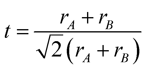
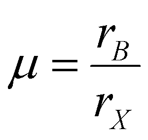
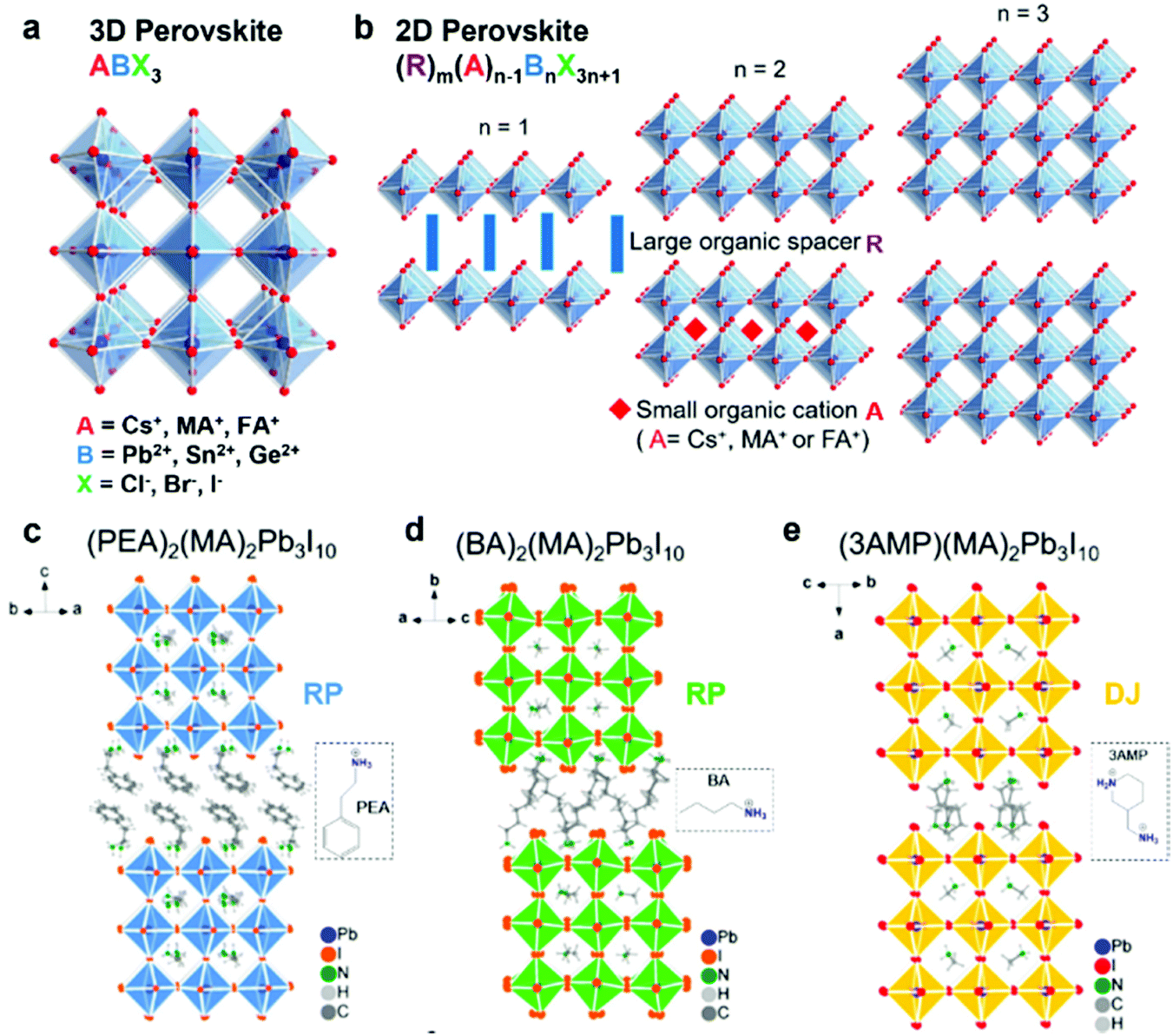
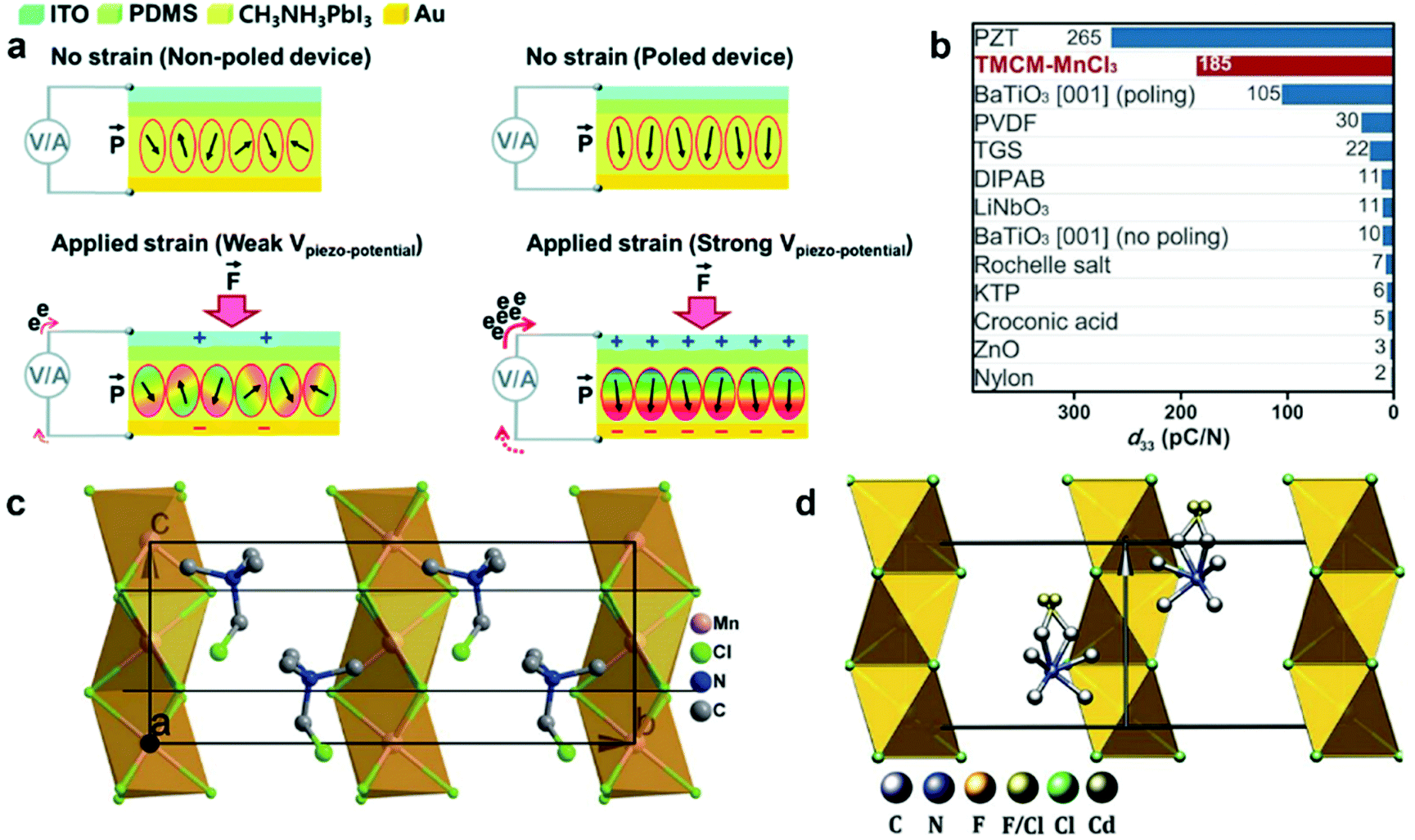
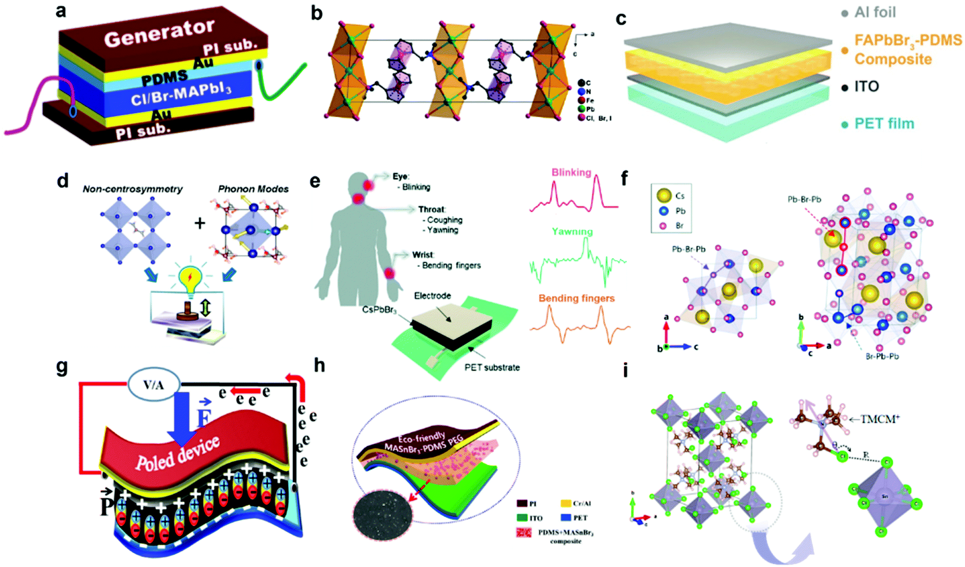

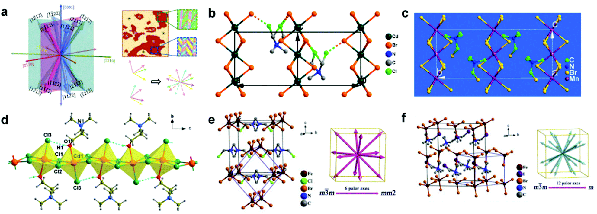
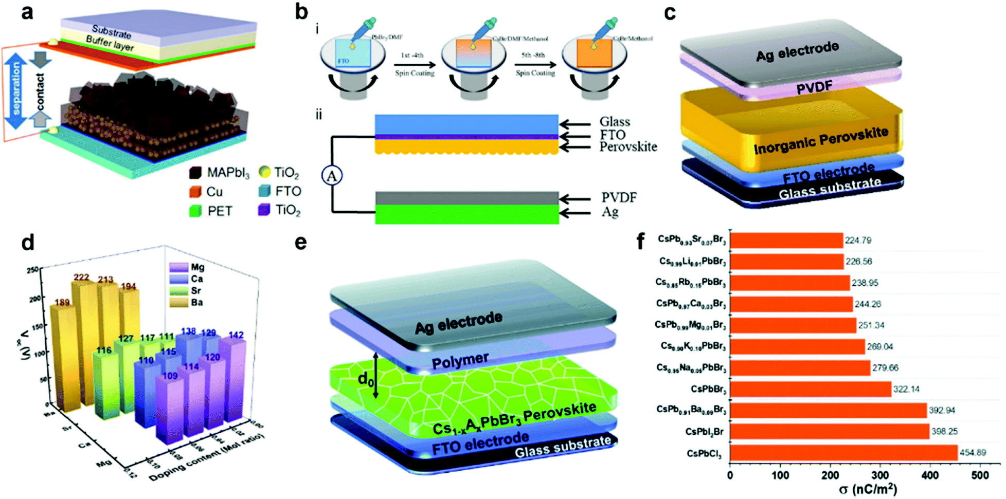
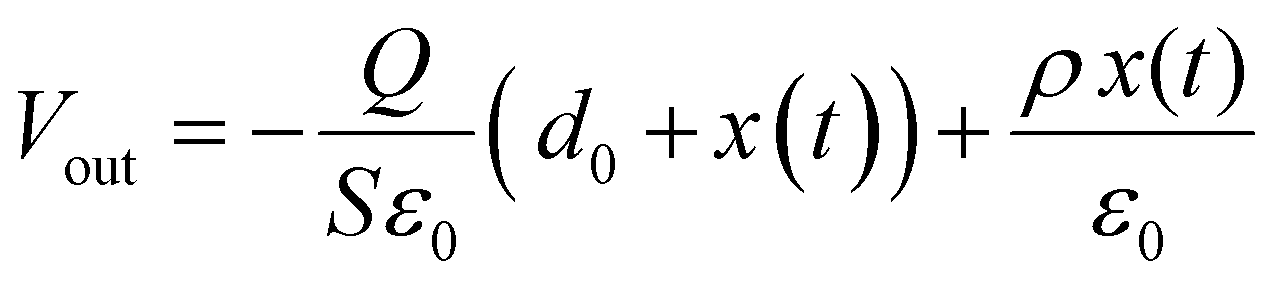
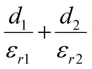 for the dielectric-to-dielectric contact mode and
 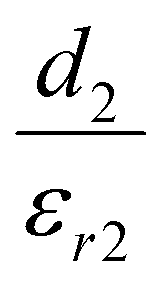 for the conductor-to-dielectric contact mode (d1, d2, εr1 and εr2 are the thickness of material 1 (dielectric or conductive material) and material 2 (dielectric material), and the dielectric constant of material 1 and material 2).