
Designing a self-classifying smart device with sensor, display, and radiative cooling functions via spectrum-selective response†
Sang Yeop
Lee
 a,
Hangyu
Lim
a,
Jung Ho
Bae
a,
Dongwoo
Chae
a,
Taejong
Paik
b,
Heon
Lee
*a and
Soong Ju
Oh
*a
a,
Hangyu
Lim
a,
Jung Ho
Bae
a,
Dongwoo
Chae
a,
Taejong
Paik
b,
Heon
Lee
*a and
Soong Ju
Oh
*a
aDepartment of Materials Science and Engineering, Korea University 145, Anam-ro Seongbuk-gu, Seoul, 02841, Republic of Korea. E-mail: heonlee@korea.ac.kr; sjoh1982@korea.ac.kr
bSchool of Integrative Engineering, Chung-Ang University, Seoul, 06974, Republic of Korea
First published on 29th July 2022
Abstract
This paper presents a self-classifying smart device that intelligently differentiates and operates three functions: electroluminescence display, ultraviolet light sensor, and thermal management via radiative cooling. The optical and electrical properties of the materials and structures are designed to achieve a spectrum-selective response, which enables the integration of the aforementioned functions into one device without any noise or interference. Spectrum-selective materials that absorb, emit, and radiate light with ultraviolet to mid-infrared wavelengths and device structures designed to prevent interference are achieved by using thin metal films, dielectric layers, and nanocrystals. The designed self-classifying smart device exhibits bright blue light emission upon current supply (display), green light emission upon exposure to UV light (sensor), and radiative cooling (thermal management). Furthermore, a smart device and house system with a display, UV light sensor, and radiative cooling performance was demonstrated. The findings of this study open new avenues for device integration in next-generation wearable device fabrication.
New conceptsHere, we introduce a self-classifying smart device that integrates a display, an ultraviolet sensor, and radiative cooling functions. The self-classifying device can detect, differentiate and determine various input signals by itself and output a different signal according to the input signal without the need for external power, circuits, and data processing. The device is designed with optically and electrically engineered materials of metals and dielectric films and nanocrystals, achieving a spectrum-selective response from ultraviolet to mid-infrared wavelength. This enables the three functions of a display that emits blue light in response to an alternating current, a sensor that emits green light upon exposure to UV light, and radiative cooling without any interferences. The self-classifying smart device opens new horizons in next-generation wearable device and sensor systems. |
Introduction
Recently, with increasing interest in the Internet of Things, research on sensor systems with various functions is being actively conducted.1–6 For the effective use of sensor systems, it is necessary to develop integrated devices with sensors, circuits, displays, and energy management devices.7–9 Such devices detect and control signals and transfer and deliver them to users in a visual form while operating stably.10,11 As complicated devices need to be integrated on a single chip with high density, synthetic methods to miniaturize materials and devices, complicated orthogonal process or patterning methods, and signal control techniques have been extensively studied.12–17 In this regard, the physical limitations of substrates and complex fabrication processes have been identified as critical issues that need to be further addressed, particularly when these devices are applied to ultrathin wearable systems.18–20 Furthermore, as too many devices are integrated into a limited substrate, thermal management becomes crucial for a stable device operation.21–23 These issues are challenging from the research, industrial, and economic perspectives, limiting the development of smart sensor systems.24,25 To fundamentally overcome the physical limitations and facilitate the integration process, it is necessary to develop a single smart device that collects various data inputs and delivers them to the user in an appropriate form via a display in a single element. If a single device can detect, classify, and present these signals to the user, the number of devices, circuits, and fabrication processes for integrating devices will be reduced. Moreover, it would be ideal if heat could be dissipated without incurring additional energy consumption via appropriately designed materials and structures. This would allow a continuous device operation with optimum performance for an extended period of time, thus avoiding any further inconvenience to the user.26–28 However, the development of a smart device that integrates these functions is structurally and materially complex, and insufficient research has been conducted on this topic to date.29,30Herein, we introduce a self-classifying smart device that integrates a display, an ultraviolet (UV)-light-detecting sensor, and zero-energy radiative cooling capabilities as a proof of concept. The self-classifying device can classify and determine three input signals by itself and output different functions according to the input signal without external power, circuits, and data processing. As the self-classifying device itself judges the input signals and displays different result outputs, users do not need any other operation tools. The device, which integrates these three functions, was designed with optically engineered materials and structures for the spectrum-selective absorption or emission of radiation from UV light with visible to mid-infrared wavelengths. The spectrum-selective optical response of the designed self-classifying structure enables the emission of blue light in response to an alternating current (AC) (display function) and green light upon exposure to UV light (sensor function), along with thermal management involving the reflection and emission of visible and mid-infrared light, respectively, (cooling function). These three functions are integrated into a single device on a flexible substrate without any noise or interference from the solution process. We demonstrate the effectiveness of the multifunctional device and smart-house system with UV light detection, display, and radiative cooling capabilities. We believe that this multifunctional smart device, fabricated without complicated processes, pioneers a new era in device integration and presents new possibilities for application in wearable devices (including devices directly applied on the human skin) and robotics.
Results and discussion
We propose a self-classifying smart device by comprehensively considering the optical, electrical, and dielectric properties of the phosphors, medium, and electrode materials, as well as the device structure. The proposed device mechanism is described in Fig. 1. First, the device display emits electroluminescence (EL) light in response to an AC using Cu-doped ZnS as a blue-light EL phosphor and a polydimethylsiloxane (PDMS) composite between the top and bottom electrodes as the active layer (Fig. S1a, ESI†). When an AC flows, electrons accelerated by the AC cause impact excitation on the Cu-doped ZnS surface, which emits blue EL light at 450 nm (Fig. S1b and c, ESI†).31–33 Second, band-engineered core/shell nanocrystals (NCs) are incorporated into the PDMS active layer of the display, acting as photoluminescence (PL) phosphors in UV light detection sensors. We designed the band structure of the NCs such that the NCs respond only to UV light to indicate whether the user has been exposed to UV light and emit light at 527 nm (green) to distinguish them from the display light at 450 nm (blue). To satisfy these conditions, we utilized the Stokes shift phenomenon, namely, the difference between the energy of the absorbed light and that of the emitted light. Because the relative volume of the shell (ZnS) is much larger than that of the core (CdSe), most of the energy absorption occurs in the shell. The UV light absorbed by the ZnS shell is transferred to the CdSe core and emitted as green light.34–36 Thus, the UV light sensor/display composite selectively converts UV light to green without reacting to the EL light. Third, a zero-energy radiative cooling function was incorporated by designing the materials to selectively respond to particular regions of the light spectrum. Visible light should be reflected to minimize heating, and mid-infrared (8–13 μm) light should be absorbed and emitted to space to maximize cooling.37–40 We selected an Ag thin film as the bottom electrode of the device to maximize the reflection of visible light and indium tin oxide-coated polyethylene terephthalate (ITO PET) as the transparent top electrode. PDMS, which is an excellent mid-infrared emitter and transparent visible medium, was selected as the active layer of the sensor/display composite.41 By using Ag, ITO PET, and PDMS, an excellent zero-energy radiative cooling performance was realized. It should be emphasized that these materials were selected and designed to minimize noise coupling and interference and maximize each function. For example, electrically conductive and optically reflective Ag thin films act as the bottom electrode (for display) and visible-light reflectors (for cooling). Optically transparent and electrically insulating PDMS acts as an active medium for the dielectric layer (for sensor and display) and a mid-infrared emitter (for cooling). The Cu-doped ZnS acts as an EL phosphor, emitting blue light in response to the AC (for display), and the optically engineered core/shell NCs act as a PL phosphor, emitting green light (for sensor). Finally, the optically transparent and electrically conductive ITO PET acts as a visible-light-transmitting layer and as the top electrode. Based on these materials and structures, the three functions, i.e., display, sensor, and zero-energy radiative cooling, can be integrated into one device.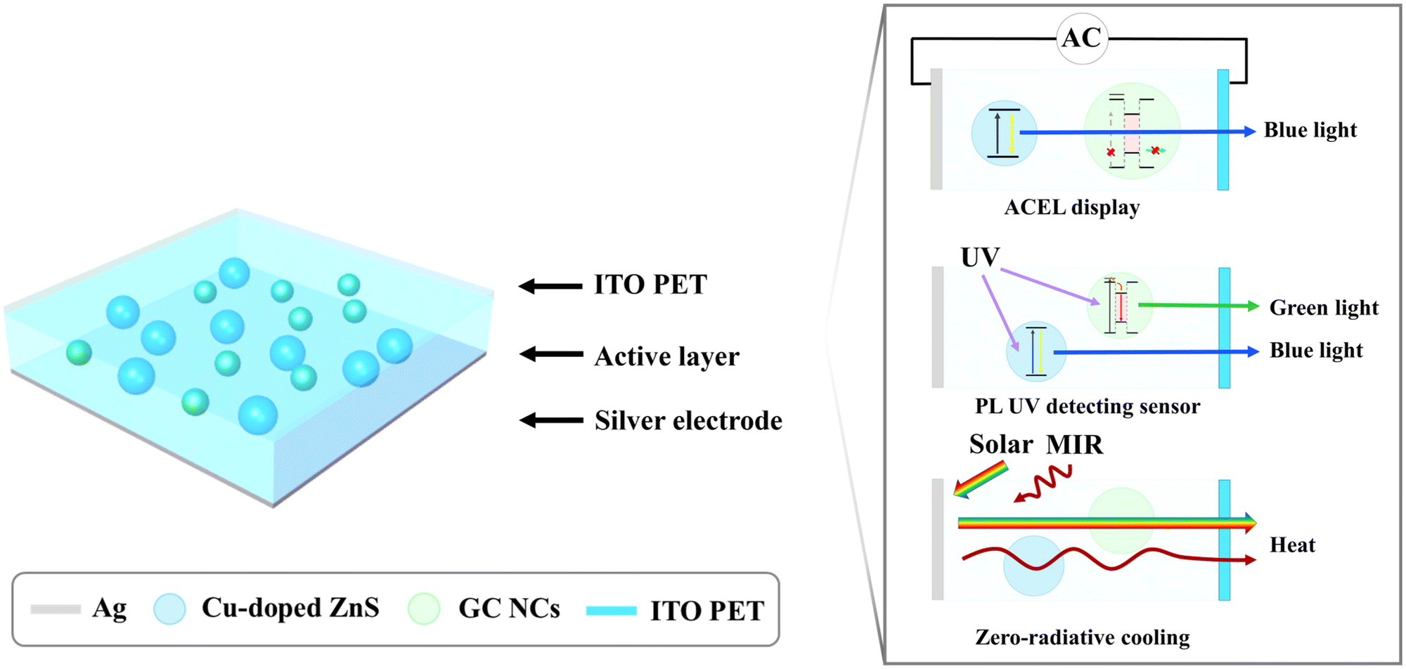 | ||
| Fig. 1 Structure and mechanism of the proposed smart device. | ||
We synthesized NCs having a green-light-emitting CdSe core and a UV-light-absorbing ZnS shell structure. The core/shell NCs were band-engineered to emit green light at 527 nm under UV light but not under visible light (Fig. 2a). NCs absorbing UV light and maximizing the Stokes shift to emit visible light were designated as giant core-shell nanocrystals (GCs).
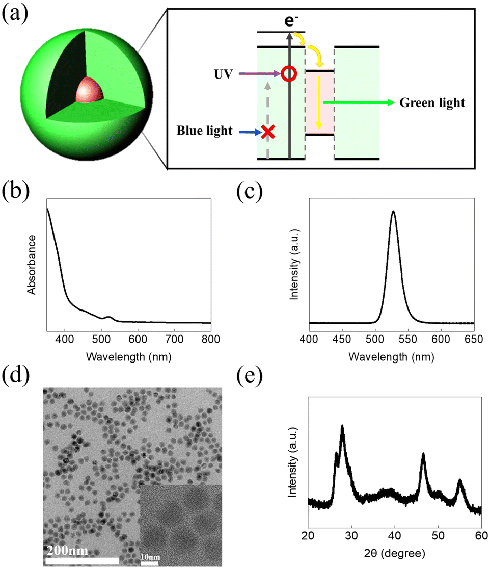 | ||
| Fig. 2 (a) Photoluminescence property, (b) UV-vis absorption spectrum, (c) PL spectrum, (d) HR-TEM image, and (e) XRD pattern of the giant core/shell nanocrystals. | ||
The optical properties of GCs were analyzed via UV-vis and PL spectroscopy (Fig. 2b and c). The UV-vis spectrum shows that absorption starts at a wavelength of approximately 400 nm. This result is in good agreement with the bandgap of ZnS.34 The PL spectrum shows an emission peak at 527 nm with a narrow full width at a half maximum of 22 nm, which corresponds to the core CdSe. There is a difference of approximately 127 nm between the onset of absorption and the PL peak, indicating a large Stokes shift. This supports the fact that the core CdSe does not absorb light because the volume ratio of the shell is very large; light is absorbed only in the ZnS shell, and only the core CdSe emits light owing to the band offset. High-resolution transmission electron microscopy (HR-TEM) and X-ray diffraction (XRD) measurements were used to investigate the structural properties of the synthesized GCs (Fig. 2d). The HR-TEM image shows that the GCs have a typical diameter of 13 nm and their size distribution is very narrow. In addition, a core size of 3 nm was observed (inset), with the ZnS shell being very large compared with the CdSe core. In addition, the XRD pattern was well matched with the 13 nm GC structure (Fig. 2e).34 The PL quantum yield of the GCs and the optical properties of the Cu-doped ZnS are provided in the ESI.†
The device fabrication process is shown in Fig. 3a. A 200 nm Ag layer produced via thermal evaporation was used as the bottom electrode on the PET substrate. A PDMS composite (1 wt% ZnS, 0.1 wt% GC) was spin-coated to a thickness of 100 nm onto the Ag-deposited PET and then half-cured. ITO PET was placed on the half-cured PDMS to form the top electrode, which was then completely cured.
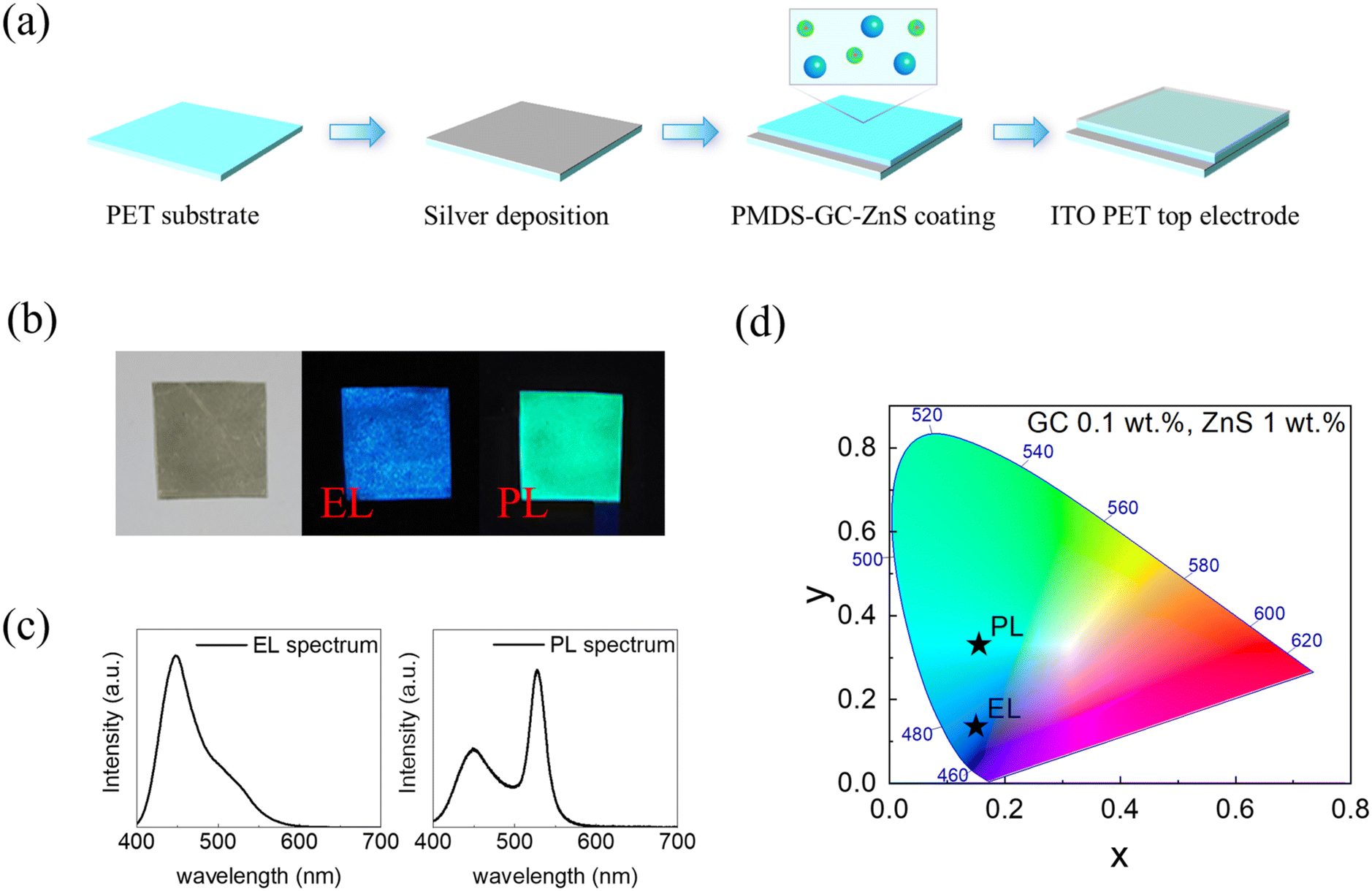 | ||
| Fig. 3 (a) Fabrication process of the proposed smart device. (b) Images of the smart device under white light (left), AC with blue EL light (middle), and UV light with green PL light (right). (c) EL spectrum of blue light under AC (left) and PL spectrum of green light under UV light (right). (d) CIE coordinates of the smart device under EL and PL light according to AC and UV light. | ||
Additionally, the performance of the smart device was analyzed. As seen in the optical image (Fig. 3b, left), the device has a mirror-like appearance under normal conditions. When the AC flows, only the Cu-doped ZnS selectively emits blue light (Fig. 3b, middle). In the absence of an AC, the GCs can also emit light under 365 nm-wavelength UV illumination, and the device then emits green light (Fig. 3b, right, and Fig. S4, ESI†). The optical properties of the fabricated device were measured using spectroscopy. When the AC flows, the device emits 450 nm (blue light), as seen in the EL spectrum (Fig. 3c, left). By contrast, under UV light, the PL emission spectrum of the GCs (Fig. 3c, right) clearly shows a peak at 527 nm (green light). In the Commission Internationale de l’ Éclairage (CIE) 1931 color coordinate system, blue light emission under an AC corresponds to the coordinates (0.1508, 0.1334) and green light emission under UV light corresponds to (0.1561, 0.3292) (Fig. 3d). The spectra and CIE coordinates show that the device clearly emits different colors of light under AC stimulation and UV illumination.
The cooling performance of the smart device was investigated by measuring the optical properties of the light-absorbing materials (Fig. S5, ESI†). Although visible light absorption should be minimized to achieve the best cooling performance, the introduction of ZnS or GCs slightly increases the UV/visible light absorption.42 The effect of ZnS on visible light absorption and cooling performance was investigated using UV-vis spectroscopy (Fig. 4a). The visible light absorption at 550 nm for the EL device containing 10 wt% ZnS in the PDMS composite was measured to be 9.594%. By contrast, the visible light absorption of the EL device containing 1 wt% ZnS was 8.068% and that of the 0.1 wt% EL device was 7.835%. An EL device with 10 wt% ZnS cannot be used for the device because its visible light absorption is too high. The EL spectrum of each device was measured using a PL spectrometer (Fig. S6, ESI†). The device with 10 wt% Cu-doped ZnS emits intense blue light, while the device with 0.1 wt% ZnS emits very weak blue light. Accordingly, the proportion of ZnS required for a sufficiently high blue light EL intensity and sufficiently low visible light absorption in a cooling device was determined to be 1 wt%.
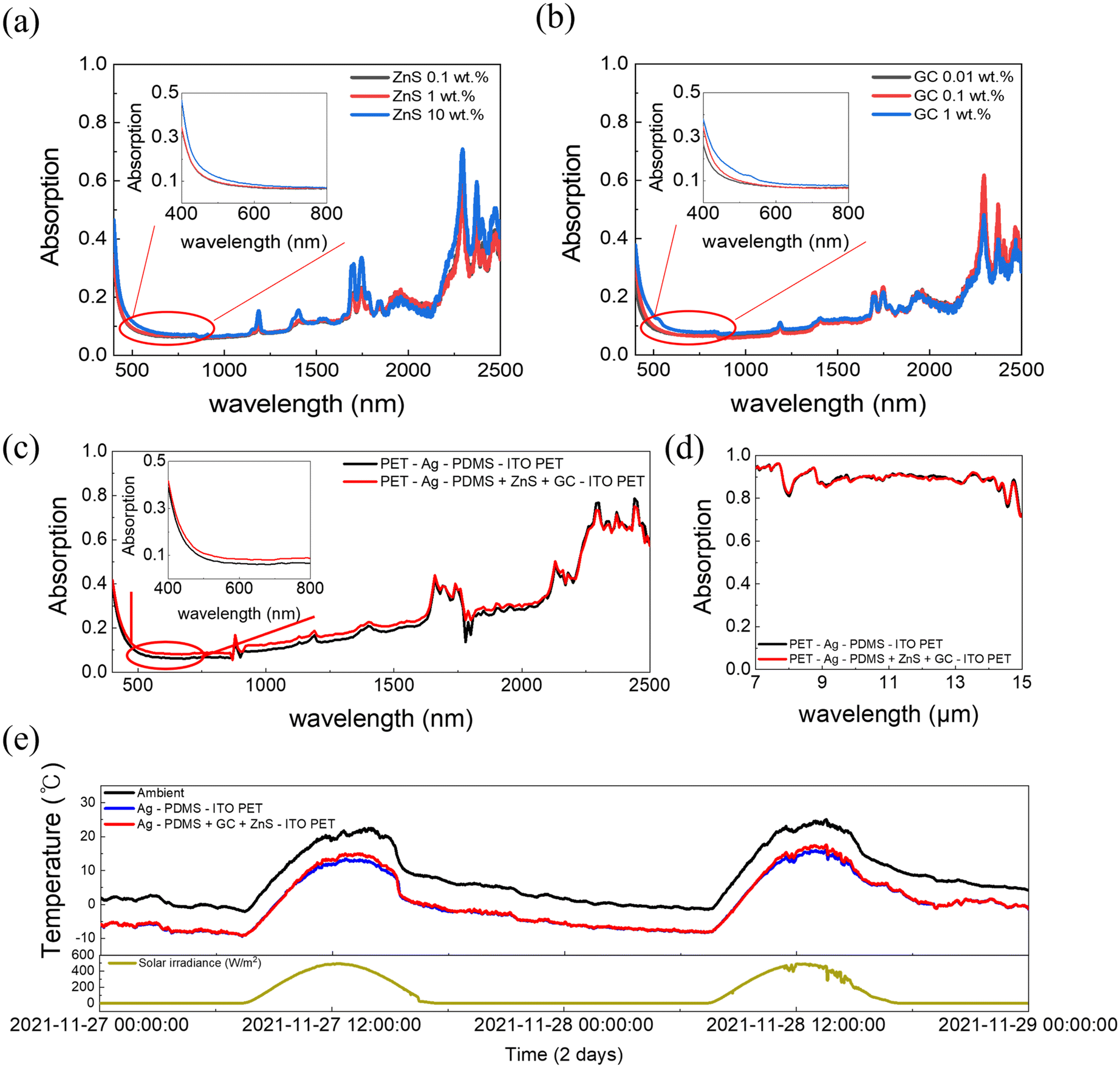 | ||
| Fig. 4 Absorption spectra of the 400–2500 nm wavelength according to (a) ZnS concentration, (b) GC concentration, and (c) device structure. (d) Absorption spectra of the two device structures between 7 and 15 μm. (e) Outdoor temperature measurement difference between the two devices, ambient temperature, and solar irradiance spectrum. | ||
Using the same method, the amount of GCs needed to achieve a satisfactory cooling performance and PL ability was investigated. Devices containing 1, 0.1, and 0.01 wt% of GCs in the PDMS composite were fabricated, and a UV-vis spectrometer was used to measure the visible-light absorption of each device (Fig. 4b). The visible light absorption at 550 nm was found to be 10.452%, 8.205%, and 7.929% for the 1, 0.1, and 0.01 wt% GC devices, respectively. Hence, a device with 1 wt% GC cannot be used owing to excessive visible light absorption. In addition, a PL spectrometer was used to investigate whether the PL intensity was sufficiently high (Fig. S7, ESI†). The PL spectrum showed that a device containing 0.01 wt% GC cannot be used because the PL intensity is too low. As a result, it was determined that 0.1 wt% GC provided a sufficiently low visible light absorption to have an acceptable cooling performance and sufficiently high PL intensity to be used in devices.
Therefore, the device was fabricated using 1 wt% ZnS and 0.1 wt% GC based on the light absorption and EL/PL spectrum intensity. A UV-vis spectrometer was used to measure the visible light absorption (Fig. 4c). A radiative cooling device with the same structure but without GC and ZnS was fabricated for visible-light absorption comparison. At 550 nm, the radiative cooling device without ZnS and GC had a visible light absorption rate of 7.031%, whereas the proposed device had a rate of 9.032%. The visible-light absorption of the proposed device was higher because ZnS absorbs visible light, and scattering occurred because of the presence of ZnS and GC in the PDMS active layer. However, a 9.032% visible-light absorption rate is still sufficiently low to allow the use of this material for cooling. The UV-vis spectrometric results thus indicate that the device can be used for cooling during daytime usage owing to its low visible light absorption.
To measure the cooling performance at night, the absorption rate at the mid-infrared wavelength was measured using a Fourier transform infrared (FT-IR) spectrometer (Fig. 4d). The mid-infrared absorption rate in the 8–13 μm range exceeded 80%, which is sufficiently high for the device to be used as a cooling material. Based on the mid-infrared absorption, an acceptable cooling performance could result from effective heat exchange with space during usage at night.
Outdoor measurements were performed to investigate the external cooling characteristics of the fabricated smart devices. A chamber that could measure several samples simultaneously was used to measure the cooling performance of the device (Fig. S8, ESI†). The size of the chamber for measuring each sample was the same, and the top was covered with a polyethylene film to minimize the influence of wind.
The cooling performance of the device under solar irradiation for two days was measured using this chamber (Fig. 4e). During the daytime, the radiative cooling device without Cu-doped ZnS and GC was cooled by 10.6 °C, whereas the proposed device was cooled by 9.6 °C. The cooling performance of the proposed device during the daytime was weakened by the solar energy absorption by the Cu-doped ZnS and GC. At night, when solar energy absorption by the ZnS and GC did not occur, both samples were cooled by 8.6 °C. The excellent radiative cooling performance of the proposed smart device was thus verified via outdoor temperature measurements. Other data to verify the cooling performance, such as the wind speed and cooling power, are described in the ESI.†
The proposed smart device can distinguish between UV and AC by the different colors of the PL and EL light. Depending on which of the device's layers is patterned through lithography during the fabrication process, two devices can be fabricated: a ‘display’ mode device, which emits blue light of a specific pattern under AC and green light over the entire area under UV light, and a ‘warning’ mode device, which emits green light of a specific pattern under UV light and blue light over the entire area under AC. The ‘display’ mode device is fabricated by patterning the ITO of the top electrode and via lithography and acid-etching processes, such that when the ZnS under the ITO is stimulated by the AC and emits blue light, only the pattern is displayed to the user. For example, on the device shown in Fig. 5a, the ITO top electrode was patterned with the word ‘cool,’ and only the ZnS below the remaining ITO emitted blue light. However, the GC was not patterned; therefore, the entire area emitted green PL light when exposed to UV light. According to the pattern on the ITO, various shapes of information can be displayed in the form of blue light.
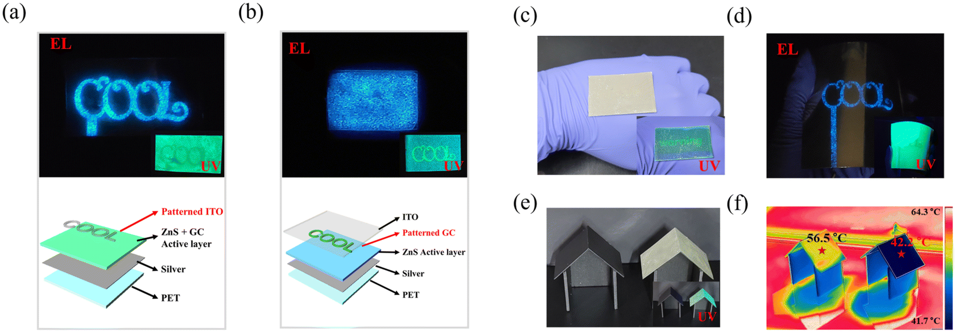 | ||
| Fig. 5 (a) Image of a smart device under AC (top) and UV light (inset) and device structure (bottom). (b) Image of another smart device under AC (top) and UV light (inset) and device structure (bottom). (c) Image of the smart device under white and UV light (inset). (d) Image of a flexible large smart device. (e) Image of imitation houses with a conventional roof (left) and a smart-device roof (right), and under UV light (inset). (f) Infrared image of imitation houses with a conventional roof (left) and a smart-device roof (right) outdoors during the daytime. | ||
Alternatively, in the ‘warning’ mode, the GC in the active layer is patterned (Fig. 5b), but the ITO remains over the entire area of the device, such that when the AC is applied, blue EL light is emitted over the entire area. However, when the device is exposed to UV light, only the GC area that remains unpatterned emits green light. Thus, it is possible to effectively inform the user that UV light exists by means of an intuitive shape or text.
The device uses Ag coated on PET as the bottom electrode, PDMS with very good flexible properties for the active layer, and ITO PET as the top electrode. By using the spin coating method, it can be fabricated with a large area. Furthermore, as both the substrate and active layer have very good flexibility, a ‘warning’ mode and large ‘display’ mode smart device with excellent flexible characteristics can be fabricated and used in wearable applications (Fig. 5c, d and Fig. S13, ESI†).
A miniature ‘house’ system comprising a plain house and a smart house was constructed to simultaneously demonstrate the sensing and cooling performance (Fig. 5e and f). Unlike the plain house, the fabricated smart house emitted bright green PL light under UV light. The plain and smart houses were placed outside during the daytime, and their temperatures were measured using an infrared camera. After 30 min, the temperatures of the plain and smart houses were 56.5 and 42.2 °C, respectively, revealing that the smart house effectively exhibited a cooling performance of 14.3 °C during the daytime.
Conclusions
This paper presents a smart device with electroluminescence display, UV light sensor, and thermal management via radiative cooling using optically and electrically engineered material properties and device structures. The proposed self-classifying smart device achieved spectrum-selective response and self-classifying characteristics, thereby successfully classifying the input signals of AC and UV light. The smart device showed green or blue output light without any interference according to the incoming signal and exhibited radiative cooling performance in an outdoor environment. Two device modes specialized to distinguish between AC and UV light were successfully fabricated by selectively patterning the materials, and a smart-house model system with radiative cooling performance was fabricated. This study presents a fundamental concept for engineering material properties and device structures and provides insight into the utilization of next-generation smart devices.Materials and methods
Materials
Cadmium acetate hydrate (99.99%; trace metal basis), selenium (99.99%; trace metal basis), sulfur (99.998%), zinc acetate dihydrate (≥98%), zinc oxide (≥99.0%; ACS reagent), 1-octadecene (tech; 90%), oleic acid (90%), indium tin oxide-coated PET (60 Omega sq−1), hexane (anhydrous; 95%), acetone (≥99.8%; suitable for HPLC), and MIF 300k developer (tetramethylammonium hydroxide) were purchased from Sigma-Aldrich. Trioctylphosphine (TOP; 90%; technical grade) was purchased from Acros Organics (USA). Hydrochloric acid (35–37%) and nitric acid (60%) were purchased from Samchun. Polydimethylsiloxane (Sylgard 184) was purchased from K1 Solution. Zinc sulfide (99.99%; activated CuCl-doped; phosphorescent grade) was purchased from NET. A silver thermal evaporation source (99.99%) was purchased from iTASCO. AZ GXR-601 (14CP) was purchased from AZ Electronic Materials. Cooluv-100 UV was purchased from Jaesung Engineering. The PET film was purchased from SKC.Giant core/shell NC (GC) synthesis
Cadmium acetate hydrate (0.21 mmol), zinc oxide (5.115 mmol), and oleic acid (10.5 mL) were placed in a 3-neck flask, degassed for 1 h, and heated to 150 °C in an N2 atmosphere. A 22.5 mL portion of 1-octadecene (ODE) was then injected and the mixture was heated to 310 °C. A stock solution was prepared by dissolving 3.3 mmol of Se and 3.3 mmol of S in 3.3 mL of TOP, and this solution was injected into the above mixture in the 3-neck flask and the temperature was maintained for 10 min. A zinc stock solution (4.29 mmol of zinc acetate dihydrate, 1.15 mL of oleic acid, and 6 mL of ODE) was injected into the above mixture. Afterward, a sulfur stock solution (14.475 mmol sulfur in 7.5 mL of TOP) was injected dropwise. The mixture was then maintained at 270 °C for 20 min. After centrifugation, the GCs were dispersed in hexane.Self-classifying smart device fabrication
A PET film substrate was cleaned using acetone, ethanol, and distilled water with sonication. A 200 nm-thick Ag bottom electrode was deposited using a thermal evaporator. PDMS was prepared by mixing the curing agent and base in a weight ratio of 1![[thin space (1/6-em)]](https://www.rsc.org/images/entities/char_2009.gif) :10. After mixing, 0.1 wt% of GCs and 1 wt% of Cu-doped ZnS were added to the PDMS, which was then kept under vacuum in a desiccator for 1 h. The PDMS, GCs, and Cu-doped ZnS mixture was spin-coated at 1000 rpm for 30 s onto the Ag-deposited PET film and then half-cured at 80 °C for 30 min. The ITO PET top electrode was placed on the half-cured PDMS mixture and curing was completed by heating at 80 °C for 1 h. A radiative-cooling device was fabricated using the same process without the GCs and Cu-doped ZnS. The smart device was operated at 100 V AC and 500 Hz.
:10. After mixing, 0.1 wt% of GCs and 1 wt% of Cu-doped ZnS were added to the PDMS, which was then kept under vacuum in a desiccator for 1 h. The PDMS, GCs, and Cu-doped ZnS mixture was spin-coated at 1000 rpm for 30 s onto the Ag-deposited PET film and then half-cured at 80 °C for 30 min. The ITO PET top electrode was placed on the half-cured PDMS mixture and curing was completed by heating at 80 °C for 1 h. A radiative-cooling device was fabricated using the same process without the GCs and Cu-doped ZnS. The smart device was operated at 100 V AC and 500 Hz.
“Display” mode smart device fabrication
The AZ GXR-601 photoresist was spin-coated onto the ITO PET at 3000 rpm for 30 s and annealed at 100 °C for 3 min. After annealing, the photoresist was exposed to UV for 12 s. The developing process using the MIF 300k developer was conducted for 45 s, and the remaining photoresist was annealed at 100 °C for 30 min. The ITO was etched by dipping it for 10 s into an acid solution composed of distilled water, hydrochloric acid, and nitric acid in a volume ratio of 10:9:1. After etching, the remaining photoresist was removed by washing with acetone. The PET substrate was cleaned and then coated with 200 nm of silver using a thermal evaporator. A PDMS mixture was prepared by mixing the base and curing agent in a weight ratio of 10:1 and then adding 1 wt% of Cu-doped ZnS and 0.1 wt% of GCs to the PDMS. This mixture was spin-coated onto the silver layer and cured at 80 °C for 30 min. After half-curing, the etched ITO PET was loaded onto the spin-coated PDMS mixture and then fully cured at 80 °C for 1 h.
“Warning” mode smart device fabrication
The PET substrate was cleaned and coated with 200 nm silver using a thermal evaporator. A PDMS mixture was prepared by mixing the base and curing agent in a weight ratio of 10:1 and 1 wt% of Cu-doped ZnS to the PDMS. The mixture of PDMS and Cu-doped ZnS was spin-coated onto the Ag layer and completely cured at 80 °C for 90 min. After curing, a giant core/shell layer was spin-coated onto the PDMS layer at 3000 rpm for 30 s, after which the AZ GXR-601 photoresist was spin-coated onto the giant core/shell layer at 3000 rpm for 30 s and annealed at 100 °C for 3 min. The layer was then exposed to UV light for 12 s, and the development process was conducted for 45 s. The remaining photoresist was removed using acetone. The PDMS adhesion layer was prepared by mixing the curing agent and base in a weight ratio of 1:10 and spin-coated on the ITO PET at 5000 rpm for 30 s. Finally, the ITO PET with the PDMS adhesion layer was loaded onto the patterned giant core/shell layer and fully cured at 80 °C for 1 h.
Characterization
The optical properties of the GCs and devices were measured using a UV-vis spectrometer (JASCO-V770) and via PL spectroscopy (FP-8500, JASCO). The PL quantum yield was analyzed via PL spectroscopy (FA-356, Thermo). The structural properties of the GCs were investigated via X-ray diffraction (XRD) (Smartlab, Rigaku), their morphological properties via transmission electron microscopy (TEM) (Tecnai G2 F30, FEI, Korea Basic Science Institute), and their electrical properties using a probe station (MST-4000A, MSTECH). The CIE coordinates of the smart devices were calculated using the chromaticity diagram application in Origin 2019b (OriginLab). The outdoor measurements of the cooling performance were performed using a hand-made outdoor chamber. The outdoor temperature was measured directly using thermocouples (K-type, ST-50, RKC Instrument) with a data logger (OM-CP-OCTTEMP-A, OMEGA Engineering). Cooling power and temperature simulations were performed using MATLAB R2021a.Author contributions
S. Y. Lee contributed to most work; H. Lee and S. J. Oh supervised the project; H. Lim assisted in the material synthesis; D. Chae and T. Paik helped in the material characterization and device analysis; J. H. Bae assisted in the smart device fabrication; S. Y. Lee and S. J. Oh drafted and revised the manuscript.Conflicts of interest
There are no conflicts to declare.Acknowledgements
This research was supported by the Creative Materials Discovery Program through the National Research Foundation of Korea (NRF) funded by the Ministry of Science and ICT (NRF-2018M3D1A1059001), the Basic Science Research Program through the National Research Foundation of Korea (NRF), funded by the Ministry of Science, ICT and Future Planning (2022R1A2C4001517), the National Research Foundation of Korea grant funded by the Korea government (2020M3H4A3081833), and the Materials Innovation Project (NRF-2021M3H4A3026733).Notes and references
- R. Yin, D. Wang, S. Zhao, Z. Lou and G. Shen, Adv. Funct. Mater., 2021, 31, 1 Search PubMed.
- G. A. Salvatore, J. Sülzle, F. Dalla Valle, G. Cantarella, F. Robotti, P. Jokic, S. Knobelspies, A. Daus, L. Büthe, L. Petti, N. Kirchgessner, R. Hopf, M. Magno and G. Tröster, Adv. Funct. Mater., 2017, 27, 1 CrossRef.
- J. Bang, W. S. Lee, B. Park, H. Joh, H. K. Woo, S. Jeon, J. Ahn, C. Jeong, T. il Kim and S. J. Oh, Adv. Funct. Mater., 2019, 29, 1 CrossRef.
- S. Jeon, J. Ahn, H. Kim, H. K. Woo, J. Bang, W. S. Lee, D. Kim, M. A. Hossain and S. J. Oh, J. Phys. Chem. C, 2019, 123, 11001 CrossRef CAS.
- F. P. Wieringa and J. P. Kooman, Nat. Rev. Nephrol., 2020, 16, 554 CrossRef PubMed.
- J. Ahn, S. Jeon, W. S. Lee, H. K. Woo, D. Kim, J. Bang and S. J. Oh, J. Phys. Chem. C, 2019, 123, 18087 CrossRef CAS.
- K. Xu, Y. Lu, T. Yamaguchi, T. Arie, S. Akita and K. Takei, ACS Nano, 2019, 13, 14348 CrossRef CAS PubMed.
- J. H. Koo, D. C. Kim, H. J. Shim, T. H. Kim and D. H. Kim, Adv. Funct. Mater., 2018, 28, 1 Search PubMed.
- K. Meng, S. Zhao, Y. Zhou, Y. Wu, S. Zhang, Q. He, X. Wang, Z. Zhou, W. Fan, X. Tan, J. Yang and J. Chen, Matter, 2020, 2, 896 CrossRef.
- K. K. Kim, I. H. Ha, M. Kim, J. Choi, P. Won, S. Jo and S. H. Ko, Nat. Commun., 2020, 11, 1 CrossRef PubMed.
- J. Park, J. Kim, S. Y. Kim, W. H. Cheong, J. Jang, Y. G. Park, K. Na, Y. T. Kim, J. H. Heo, C. Y. Lee, J. H. Lee, F. Bien and J. U. Park, Sci. Adv., 2018, 4, 1 Search PubMed.
- H. Niu, H. Zhang, W. Yue, S. Gao, H. Kan, C. Zhang, C. Zhang, J. Pang, Z. Lou, L. Wang, Y. Li, H. Liu and G. Shen, Small, 2021, 17, 1 Search PubMed.
- B. K. Jung, S. Jeon, H. K. Woo, T. Park, J. Ahn, J. Bang, S. Y. Lee, Y. M. Lee and S. J. Oh, ACS Appl. Mater. Interfaces, 2021, 13, 5 Search PubMed.
- J. Ahn, S. Jeon, H. K. Woo, J. Bang, Y. M. Lee, S. J. Neuhaus, W. S. Lee, T. Park, S. Y. Lee, B. K. Jung, H. Joh, M. Seong, J. H. Choi, H. G. Yoon, C. R. Kagan and S. J. Oh, ACS Nano, 2021, 15, 15667 CrossRef CAS PubMed.
- S. Jeon, S. Y. Lee, S.-K. Kim, W. Kim, T. Park, J. Bang, J. Ahn, H. K. Woo, J.-Y. Chae, T. Paik, T.-Y. Seong and S. J. Oh, Adv. Opt. Mater., 2020, 8, 1 Search PubMed.
- Y. Lu, K. Jiang, D. Chen and G. Shen, Nano Energy, 2019, 58, 624 CrossRef CAS.
- L. J. Currano, F. C. Sage, M. Hagedon, L. Hamilton, J. Patrone and K. Gerasopoulos, Sci. Rep., 2018, 8, 1 CAS.
- M. Zhang, X. Gao, C. Lu, D. Yao, L. Wu, D. Li, H. Fang, A. Shiwei and Y. Sun, ACS Appl. Mater. Interfaces, 2021, 13, 55735 CrossRef CAS PubMed.
- W. H. Yeo, Y. S. Kim, J. Lee, A. Ameen, L. Shi, M. Li, S. Wang, R. Ma, S. H. Jin, Z. Kang, Y. Huang and J. A. Rogers, Adv. Mater., 2013, 25, 2773 CrossRef CAS PubMed.
- Y. H. Jung, T. H. Chang, H. Zhang, C. Yao, Q. Zheng, V. W. Yang, H. Mi, M. Kim, S. J. Cho, D. W. Park, H. Jiang, J. Lee, Y. Qiu, W. Zhou, Z. Cai, S. Gong and Z. Ma, Nat. Commun., 2015, 6, 7170 CrossRef PubMed.
- C. Tan, Z. Dong, Y. Li, H. Zhao, X. Huang, Z. Zhou, J. W. Jiang, Y. Z. Long, P. Jiang, T. Y. Zhang and B. Sun, Nat. Commun., 2020, 11, 1 CrossRef PubMed.
- J. Wu, Z. Wu, Y. Wei, H. Ding, W. Huang, X. Gui, W. Shi, Y. Shen, K. Tao and X. Xie, ACS Appl. Mater. Interfaces, 2020, 12, 19069 CrossRef CAS PubMed.
- T. Park, H. K. Woo, B. K. Jung, B. Park, J. Bang, W. Kim, S. Jeon, J. Ahn, Y. Lee, Y. M. Lee, T. Il Kim and S. J. Oh, ACS Nano, 2021, 15, 8120 CrossRef CAS PubMed.
- J. Yang, R. Shi, Z. Lou, R. Chai, K. Jiang and G. Shen, Small, 2019, 15, 1 Search PubMed.
- B. Tian, W. Yao, P. Zeng, X. Li, H. Wang, L. Liu, Y. Feng, C. Luo and W. Wu, J. Mater. Chem. C, 2019, 7, 809 RSC.
- K. Choi, J. Lee, H. Choi, G. W. Kim, H. Il Kim and T. Park, Energy Environ. Sci., 2020, 13, 5059 RSC.
- W. Zhu, Y. Deng and L. Cao, Nano Energy, 2017, 34, 463 CrossRef CAS.
- H. H. Jung, J. Song, S. Nie, H. N. Jung, M. S. Kim, J. W. Jeong, Y. M. Song, J. Song and K. I. Jang, Adv. Mater. Technol., 2018, 3, 1 Search PubMed.
- Z. Rao, A. Thukral, P. Yang, Y. Lu, H. Shim, W. Wu, A. Karim and C. Yu, Adv. Funct. Mater., 2021, 2111232 Search PubMed.
- S. H. Kim, G. W. Baek, J. Yoon, S. Seo, J. Park, D. Hahm, J. H. Chang, D. Seong, H. Seo, S. Oh, K. Kim, H. Jung, Y. Oh, H. W. Baac, B. Alimkhanuly, W. K. Bae, S. Lee, M. Lee, J. Kwak, J. H. Park and D. Son, Adv. Mater., 2021, 33, 1 Search PubMed.
- J. Li, Z. Zhang, X. Luo, L. Zhu and Z. L. Wang, ACS Appl. Mater. Interfaces, 2022, 14, 4775–4782 CrossRef CAS PubMed.
- L. Wang, L. Xiao, H. Gu and H. Sun, Adv. Opt. Mater., 2019, 7, 1 Search PubMed.
- G. Lee, M. Kong, D. Park, J. Park and U. Jeong, Adv. Mater., 2020, 32, 1 Search PubMed.
- Y. Fu, D. Kim, W. Jiang, W. Yin, T. K. Ahn and H. Chae, RSC Adv., 2017, 7, 40866 RSC.
- R. García-Gutiérrez, M. Barboza-Flores, D. Berman-Mendoza, O. E. Contreras-López and A. Ramos-Carrazco, Mater. Lett., 2014, 132, 179 CrossRef.
- X. Zhong, M. Han, Z. Dong, T. J. White and W. Knoll, J. Am. Chem. Soc., 2003, 125, 8589 CrossRef CAS PubMed.
- S. Jeon, S. Son, S. Y. Lee, D. Chae, J. H. Bae, H. Lee and S. J. Oh, ACS Appl. Mater. Interfaces, 2020, 12, 54763 CrossRef CAS PubMed.
- J. Liu, J. Zhang, D. Zhang, S. Jiao, J. Xing, H. Tang, Y. Zhang, S. Li, Z. Zhou and J. Zuo, Renewable Sustainable Energy Rev., 2020, 130, 109935 CrossRef.
- D. Chae, S. Son, H. Lim, P. H. Jung, J. Ha and H. Lee, Mater. Today Phys., 2021, 18, 100389 CrossRef CAS.
- B. Zhao, M. Hu, X. Ao, N. Chen and G. Pei, Appl. Energy, 2019, 236, 489 CrossRef CAS.
- L. Zhou, H. Song, J. Liang, M. Singer, M. Zhou, E. Stegenburgs, N. Zhang, C. Xu, T. Ng, Z. Yu, B. Ooi and Q. Gan, Nat. Sustain., 2019, 2, 718 CrossRef.
- S. Park, J. Bang, B. S. Kim, S. J. Oh and J. H. Choi, Mater. Today Adv., 2021, 12, 100177 CrossRef CAS.
Footnote |
| † Electronic supplementary information (ESI) available: Supporting Information contains more equation derivations, optical properties, fabrication processes, and wind speed, relative humidity, dew point, cooling power, cooling temperature, and simulation data. See DOI: https://doi.org/10.1039/d2nh00206j |
| This journal is © The Royal Society of Chemistry 2022 |