
Image processing with a multi-level ultra-fast three dimensionally integrated perovskite nanowire array†
Swapnadeep
Poddar‡
a,
Yuting
Zhang‡
a,
Zhesi
Chen
a,
Zichao
Ma
 a,
Yu
Fu
a,
Yucheng
Ding
a,
Chak Lam Jonathan
Chan
a,
Qianpeng
Zhang
a,
Daquan
Zhang
a,
Zhitang
Song
*b and
Zhiyong
Fan
*a
a,
Yu
Fu
a,
Yucheng
Ding
a,
Chak Lam Jonathan
Chan
a,
Qianpeng
Zhang
a,
Daquan
Zhang
a,
Zhitang
Song
*b and
Zhiyong
Fan
*a
aDepartment of Electronic & Computer Engineering, The Hong Kong University of Science and Technology, Clear Water Bay, Kowloon, Hong Kong SAR, China. E-mail: eezfan@ust.hk
bState Key Laboratory of Functional Materials for Informatics, Shanghai Institute of Micro-system and Information Technology, Chinese Academy of Sciences, Shanghai, 200050, China. E-mail: ztsong@mail.sim.ac.cn
First published on 23rd May 2022
Abstract
Besides its ubiquitous applications in optoelectronics, halide-perovskites (HPs) have also carved a niche in the domain of resistive switching memories (Re-RAMs). However owing to the material and electrical instability challenges faced by HP thin-films, rarely perovskite Re-RAMs are used to experimentally demonstrate data processing which is a fundamental requirement for neuromorphic applications. Here, for the first time, lead-free, ultrahigh density HP nanowire (NW) array Re-RAM has been utilized to demonstrate image processing via design of convolutional kernels. The devices exhibited superior switching characteristics including a high endurance of 5 × 10⁶ cycles, an ultra-fast erasing and writing speed of 900 ps and 2 ns, respectively, and a retention time >5 × 10⁴ s for the resistances. The work is bolstered by an in-depth mechanistic study and first-principles simulations which provide evidence of electrochemical metallization triggering the switching. Employing the robust multi-level switching behaviour, image processing functions of embossing, outlining and sharpening were successfully implemented.
New conceptsPrevious reports on polycrystalline halide perovskite (HP) thin-film resistive RAM (Re-RAM) based neuromorphic devices could not empirically demonstrate analog processing owing to the temporally frail and jittery conduction states attributed to the material and electrical instability associated with environmentally delicate HPs. In this work, we utilized a unique device structure comprising single-crystalline nanowires (NWs) of lead-free HP, embedded in a porous alumina membrane (PAM), as the switching layer. The PAM induced electrical and material stability imparted to the NWs helped in yielding an ultra-fast writing and erasing speed of 2 ns and 900 ps, respectively, along with an unhindered endurance of 5 × 10⁶ cycles which are records for lead-free HP Re-RAMs and are among the state-of-the-art for all HP Re-RAMs reported. PAM instilled stability coupled with the monocrystallinity of the NWs resulted in controlled current injection, operating under different current compliances, which in turn produced non-overlapping and temporally robust (>5 × 10⁴ s) conduction states paving the way for analog processing. For the first time, experimentally, HP Re-RAMs were utilized in demonstrating neuromorphic processing by building convolutional kernels and analog image processing functions of outlining, embossing and sharpening were realized. This work propels HPs as analog processing materials for multifunctional applications in neuromorphic computing. |
Introduction
With the advent of big-data analytics, Internet of things (IoT) and artificial intelligence, there is an echoing demand for hardware that can emulate the processing capabilities of the human brain.1–4 Among the different non-volatile memories demonstrating processing, resistive RAMs (Re-RAMs) have attracted enormous attention owing to their compatibility with complex neural networks, low power computation, high-density integration and excellent data retention properties.5–9 Traditionally, a plethora of materials including selenides, chalcogenides, transition metal oxides, etc. have been explored as switching matrices in Re-RAMs for demonstrating brain-inspired computing.10,11 Halide perovskites (HPs), illustrious in the genre of optoelectronics and photovoltaics, have also been used recently as the switching material for Re-RAMs owing to their in-built hysteresis and abundance of charge-trapping sites and ion transit pathways.12–17 However, in the domain of neuromorphic computing, reports on HP thin film Re-RAMs empirically exhibiting processing are extremely scarce. Mostly HP thin film Re-RAMs have utilized the valence change mechanism (VCM) mode of operation to exhibit simple artificial synaptic characteristics like short term plasticity and long term potentiation and are often coupled with algorithm based simulations to show the processing potential.18–20 The limitation mainly stems from the poor material and electrical stability of the thin film which is susceptible to moisture induced attacks.21–24 Consequently the high device to device variation, poor retention of the resistance states and large scale integration challenges act as major impediments.24 Therefore, in order to accelerate HPs as potential processing materials, an up-gradation of the existing device design and demonstration of superlative memristive performance are the need of time.Herein, a HP Re-RAM device was fabricated with a lead-free, methyl ammonium bismuth iodide (MBI) nanowire (NW) array, rooted in a porous alumina membrane (PAM) sandwiched between silver (Ag) and aluminum (Al) electrodes. The MBI NW Re-RAM exhibited robust switching with an ON/OFF ratio of ∼107, an ultra-fast writing and erasing speed of 2 ns and 900 ps, respectively, and an unabated endurance of 5 × 10⁶ cycles. An in-depth mechanistic study including ex situ transmission electron microscopy (TEM), time-of-flight secondary mass ion spectroscopy (ToF-SIMS) and X-ray photoelectron spectroscopy (XPS) proved the origin of the switching to be electrochemical metallization (ECM) of intruding Ag inside the body of the monocrystalline MBI NWs. First-principles ballistic transport simulations explored the varying amounts of Ag pervading the MBI NWs when operated with various current compliances, and its consequent impact on the device conductance. Empirically too, the MBI NW Re-RAM produced non-overlapping multi-level resistance states with a distinctly low device to device variation and a prolonged retention >5 × 10⁴ s. The NW devices showed ∼2 times better retention and a relatively low variation and overlap among the resistance states when compared to the thin film counterpart which is attributed to the overall PAM induced and improved electrical and material stability. A similar performance improvement was obtained for PAM based HP NW optical and electronic devices, as reported by us recently, post-instillation of material and electrical stability to the delicate HP material.25–29 For the first time, utilizing the multi-level switching behaviour, convolutional kernels were designed as a proof of concept to demonstrate the analog processing capability of ECM based MBI NW devices and perovskite Re-RAMs at large. Embossing, outlining and sharpening functions could be successfully achieved for a sundial image. All in all, this study heralds the way for HP Re-RAMs to be utilized in ultra-fast, neuromorphic processing and computing applications.
Results and discussion
Concept flow, structural and morphological study
Fig. 1a shows the Re-RAM device structure comprising MBI NWs in a PAM, clubbed between Ag and Al electrodes. Magnified illustrations of the MBI crystal structure and the ECM induced Ag filament inside the MBI NWs are shown on the top right and bottom left, respectively. Fig. 1a also depicts the concept flow portraying the image processing capability of the MBI NW Re-RAM. Image processing functions like sharpening, embossing and sobel on a picture of a flower are schematically represented. Fig. 1b shows the scanning electron microscopy (SEM) image of the MBI NWs inside the PAM of a 1 μm length. This SEM cross-section sample was prepared using the focused-ion-beam lamella preparation technique. Prior to imaging, although we used an optimal beam energy (5 kV and 63 pA) and a platinum (Pt) protection layer to minimize the beam induced damage, the halide-perovskite being a soft beam-sensitive material, minimal and partial damage could not be avoided which resulted in fragmentation of some NWs. The NWs were grown by a vapor–solid–solid-reaction (VSSR) process, reported by us previously, with an ultra-high density exhibiting a fill-ratio almost equal to 100%.30 As can be confirmed from the transmission electron microscopy (TEM) image in Fig. 1c, the diameter of an individual NW was obtained to be around ∼30–40 nm. Fig. S1 of the ESI† shows the top-view SEM image of the NWs in the PAM. The high-resolution TEM (HRTEM) image, shown in Fig. 1d, reveals the single crystallinity of the MBI NWs and a lattice spacing of 5.4 Å which matches well with the (004) plane. The X-ray diffraction (XRD) study in Fig. 1e revealed that the peaks are in perfect congruence with those of previously reported MBI thin films. As shown in Fig. 1f, the photoluminescence (PL) intensity reaches the zenith around 630 nm, which too matches well with a previous report on a MBI perovskite.31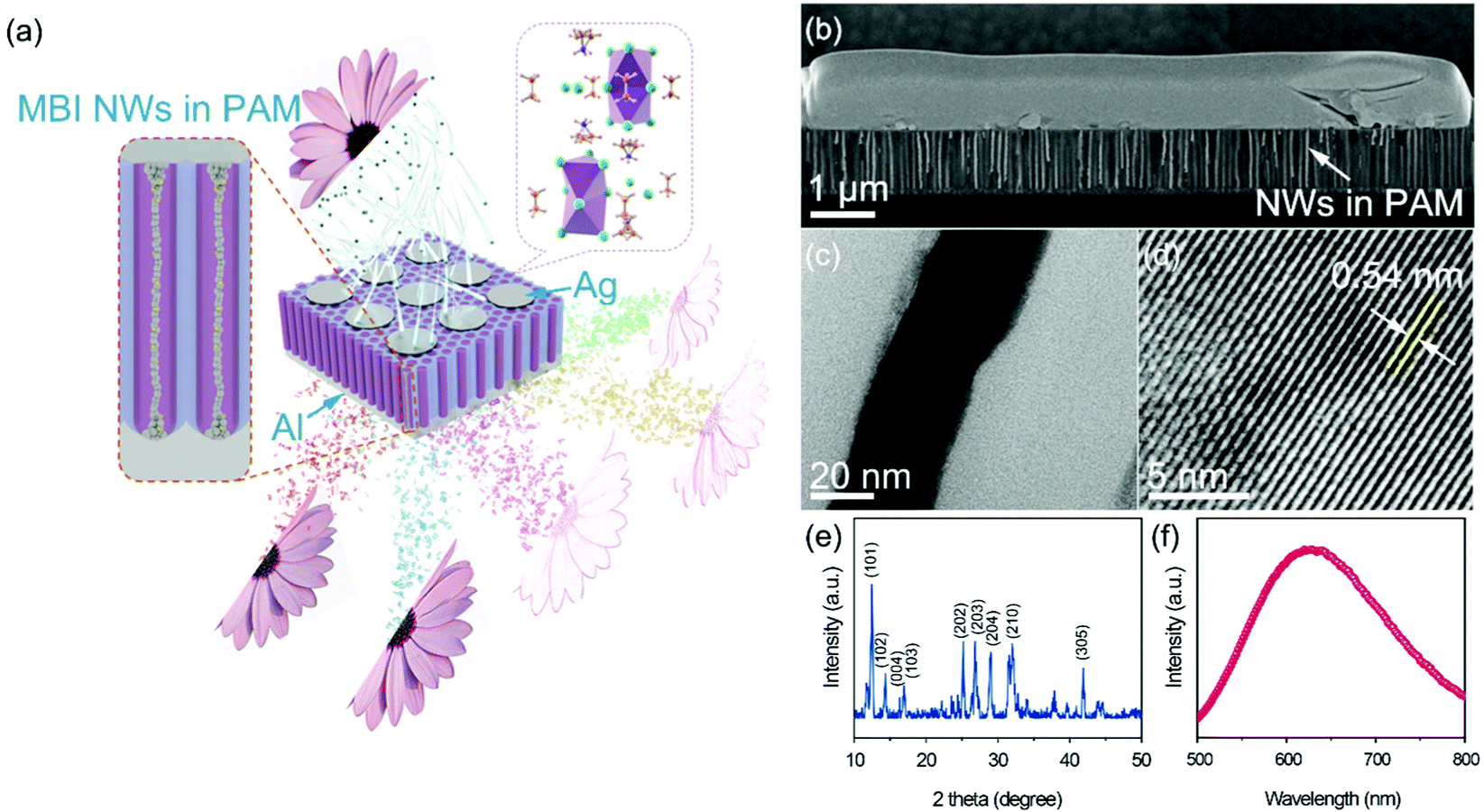 | ||
| Fig. 1 Concept flow, structural and morphological study of MBI NW Re-RAM. (a) Device structure of MBI NW Re-RAM. Concept flow showing the image processing potency of MBI NW Re-RAM exhibiting sharpening, embossing, sobel and outlining functions. Magnified images show the crystal structure of MBI (top right) and two NWs with the Ag filament triggering the ECM type of resistive switching (left). In the crystal structure, the iodide ion (shown) octahedrons with the Bi atom (not visible in the image) at the body centers are shown in violet color. The MA+ clusters are surrounding the octahedrons. (b) Cross-sectional SEM image of MBI NWs in the PAM. (c) TEM image of a single MBI NW in the PAM. (d) HRTEM image of the MBI NWs showing dominant growth along the (004) direction possessing a lattice spacing of 5.4 Å. (e) XRD spectrum of MBI NWs in the PAM. (f) PL spectrum of MBI NWs in the PAM. | ||
MBI NW Re-RAM characteristics
The I–V characteristics of the MBI NW device are shown in Fig. 2a. A voltage sweep over the range of 0 V → 6 V → −3 V → 0 yielded a transformation from the high resistance state (HRS) to the low resistance state (LRS) at 2.5 V and a jump from the LRS to the HRS at −2.1 V. The subsequent cycles exhibited a smaller requisite threshold field for switching, hinting at a filament formation mechanism guiding the resistive switching process. A large ON/OFF ratio of 107 was obtained which paved the way for reading out non-overlapping multiple resistance levels, as will be discussed later. A detailed statistical study on a batch of 15 MBI NW Re-RAM devices was carried out, as can be seen from Fig. S2 of the ESI.† A mean SET voltage of 2.4 V and a RESET voltage of −1.85 V were obtained for the devices (see Fig. S2a and b, ESI†). As shown in Fig. S2c and d (ESI†), the devices exhibited a mean LRS and HRS current of 26.5 mA and 3.8 nA, respectively.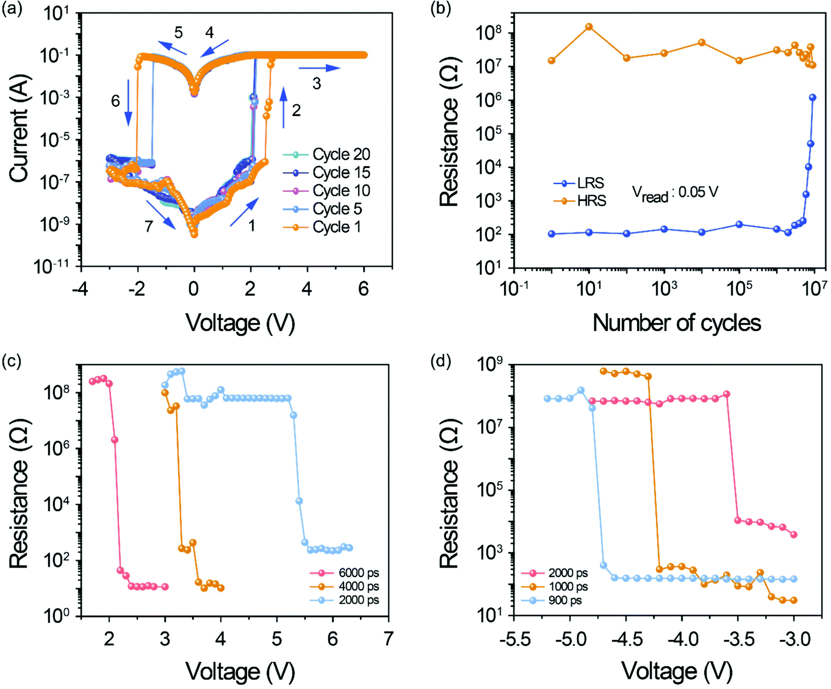 | ||
| Fig. 2 MBI NW Re-RAM characteristics. (a) I–V characteristics of MBI NW Re-RAM. (b) Cyclic endurance of MBI NW Re-RAM demonstrating a maximum endurance of 5 × 10⁶ cycles. (c) Writing speed plot of MBI NW Re-RAM exhibiting the fastest writing speed of 2 ns. (d) Erasing speed plot of MBI NW Re-RAM exhibiting an erasing speed of 900 ps. | ||
The electrical robustness of the MBI NW Re-RAM was tested by a cyclic endurance with a pulsed voltage train of 0.05 V/9 V/0.05 V/−9 V/0.05 V amplitude and a pulse width of 100 μs. An unhindered endurance performance of 5 × 10⁶ cycles was obtained after which the LRS gradually degraded towards the HRS as can be seen from Fig. 2b. Such a high endurance of the MBI NW Re-RAM is attributed to the electrical and material robustness imparted by the PAM. The cumulative probability plot of the endurance is provided in Fig. S3a of the ESI† which depicts the non-overlapping of the LRS and HRS up to 5 × 10⁶ cycles. Fig. S3b (ESI†) shows the statistical study on a batch of 15 devices with a mean endurance value of 2.3 × 10⁶ cycles.
The DC endurance test for the MBI NW based Re-RAMs was performed using I–V sweep scans (0 V → 6 V → −3 V → 0 V; 1 mA current compliance). The devices could run unabated for 5000 cycles without any tangible drop in the ON/OFF ratio at a read voltage of 0.05 V. The extracted HRS/LRS values are plotted in Fig. S4 of the ESI.†
The switching speed measurement was carried out on the MBI NW Re-RAM devices by application of sub-ns and ns switching pulses and reading out the resistance of the device before and after the application of the pulses. The circuit design for the switching speed study is provided in Fig. S5a (ESI†). Fig. 2c and d shows the fastest writing speed obtained to be 2 ns at a voltage of 5.3 V and the fastest erasing speed to be 900 ps at a switching voltage of −4.4 V. A readout voltage of 0.05 V was used for the speed measurements. The source pulses, having a width corresponding to the obtained fastest writing and erasing speed (2 ns and 900 ps, respectively), are duly provided in Fig. S5b and c of the ESI.† Fig. S6a and b (ESI†) shows a schematic of the input pulse trains and the read voltage stress test on the MBI NW devices, respectively. An electrical stress test with DC biasing of 0.05 V for more than 5000 s did not result in any degradation of HRS towards LRS. It must be mentioned here that the obtained endurance and switching speed values are the highest and fastest for lead-free HP Re-RAMs and among the state-of-the-art for all HP Re-RAMs reported so far (see Table 1).
| Device structure | ON/OFF ratio | Endurance (cycles) | Switching speed (ns) | Retention time (s) | Neuromorphic processing demonstration |
|---|---|---|---|---|---|
| a These studies report lead-free HP Re-RAMs for data storage. b These studies report lead HP Re-RAMs for data storage. c These studies report HP based neuromorphic processing devices. | |||||
| Ag/MBI NWs/ITO (this work) | 107 | 5 × 10⁶ | 2 (W); 0.9 (E) | >5 × 10⁴ | Image processing |
| 45Au/MBI TF/ITOa | 102 | 300 | 100 (W); 100 (E) | 104 | — |
| 31Cu/MBI/ITOa | 104 | 1730 | 10 (W); 10 (E) | 3 × 10⁵ | — |
| 46Au/MAPbI3/ITOb | 400 | 100 | 1000 (W); 1000 (E) | 104 | — |
| 28Ag/MAPbI3 NWs/Alb | 107 | 6 × 10⁶ | 0.1 (W); 0.1 (E) | 6.5 × 10⁷ (extrapolated) | — |
| 47ITO/(MA/Cs/FA)PbBr3/Alc | — | — | — | >5 | Pattern recognition (simulation) |
| 13Graphene/(PEA)2PbBr4/Auc | 10 | 100 | N/A | 1000 | No demo |
| 20NiO/(C4H9NH3)2PbBr4/ZnO/FTOc | <10 | — | — | 3600 | No demo |
| 48CsBI floating gate transistorc | — | — | — | >1.4 × 10⁴ | Image recognition (simulation) |
Mechanistic study of MBI NW Re-RAM
In order to delve deep into the underlying mechanism guiding the resistive switching in MBI NW Re-RAM, TEM energy dispersive spectroscopy (EDS) mapping was conducted on the pristine NW (PNW) and switched NW (SNW), respectively. Fig. 3a–h duly shows the EDS maps of traced Ag, bismuth (Bi) and iodine (I) for the PNW and SNW in the top and bottom rows, respectively. It can be well observed that the SNW demonstrated a significantly higher concentration of mapped Ag compared to the PNW, indicating the ECM of intruded Ag within the MBI NW upon switching. Fig. 3i shows the Ag atomic concentration (%) within seven MBI PNWs and SNWs, possessing a mean of 0.024% and 1.225%, respectively. To further bolster the mechanistic study, ToF-SIMS was carried out on the SNWs and PNWs. Specifically, MBI NW Re-RAMs, on the same chip with a switching layer thickness of ∼500 nm and a Ag thickness ∼100 nm, were used for the test, such that one was switched to the LRS (SNW) and the other was made to stay at the HRS (PNW). Fig. 3j shows the ToF SIMS depth profile study of the secondary CsAg+ ions for the SNW and PNW devices which clearly indicated a higher intensity of secondary Ag ions within the MBI SNW device compared to the PNW counterpart. The Bi, I and Ag secondary ion intensities corresponding to a MBI PNW are also provided in Fig. S7a of the ESI.† To confirm the Ag intrusion hypothesis further, meticulous XPS studies were carried out on the MBI NW devices having a Ag thickness of ∼50 nm and a NW length of ∼150 nm. Akin to the ToF-SIMS study, the SNW demonstrated a higher atomic concentration of Ag compared to the PNW, inside the body of the MBI NWs, as can be observed from Fig. 3k. As shown in Fig. S7b (ESI†), the binding energy peak positions of Ag (3d), Bi (4f) and I (3d) at 368.4 eV, 158.2 eV and 622.2 eV for a MBI PNW device matches well with previous reports, affirming the material integrity of the device during the XPS study.32–34 The intensity vs. binding energy plots, corresponding to Ag (3d), for the PNW and SNW devices are provided in Fig. S8 of the ESI.† The intensities of the Ag0(3d)5/2 and Ag0(3d)3/2 peaks were temporally observed with gradual milling from the Ag surface into the MBI NW, with the aid of argon (Ar) milling. It can be well observed from Fig. S8a (ESI†) that the Ag0(3d)5/2 and Ag0(3d)3/2 peaks positioned at 368.4 eV and 374.3 eV did not demonstrate any shift with gradual milling down from the Ag top surface into the Ag/MBI PNW interface. In stark contrast, as can be observed from Fig. S8b (ESI†), at the Ag/MBI SNW interface, a shift occurred as the Ag0(3d)5/2 and Ag0(3d)3/2 peaks repositioned at 371.4 eV and 377.3 eV, respectively. The peak positions of the Ag (3d) binding energy for the PNW match very well with those of metallic bulk Ag as confirmed from previous reports.32 On the other hand, the upshift observed at the Ag/MBI NW interface for the SNW is an indication of the size effect coming into play rather than a change in the oxidation state of Ag which is traditionally associated with a downshift of the binding energy.32,35,36 More precisely, this interesting result indicates that, at the interface and inside the SNW, there are plausible nanoclusters (NCs) of Ag rather than a continuous bulk metal thin film.32 This hypothesis is further supported by previous reports which have attributed such upshifts of the Ag binding energy to the insubstantial and reduced screening of core holes inside tiny Ag nanoparticles or clusters.37,38 The overall observation of the XPS study in Fig. S8 (ESI†), therefore, is in congruence with the existence of ECM induced Ag inside the SNW.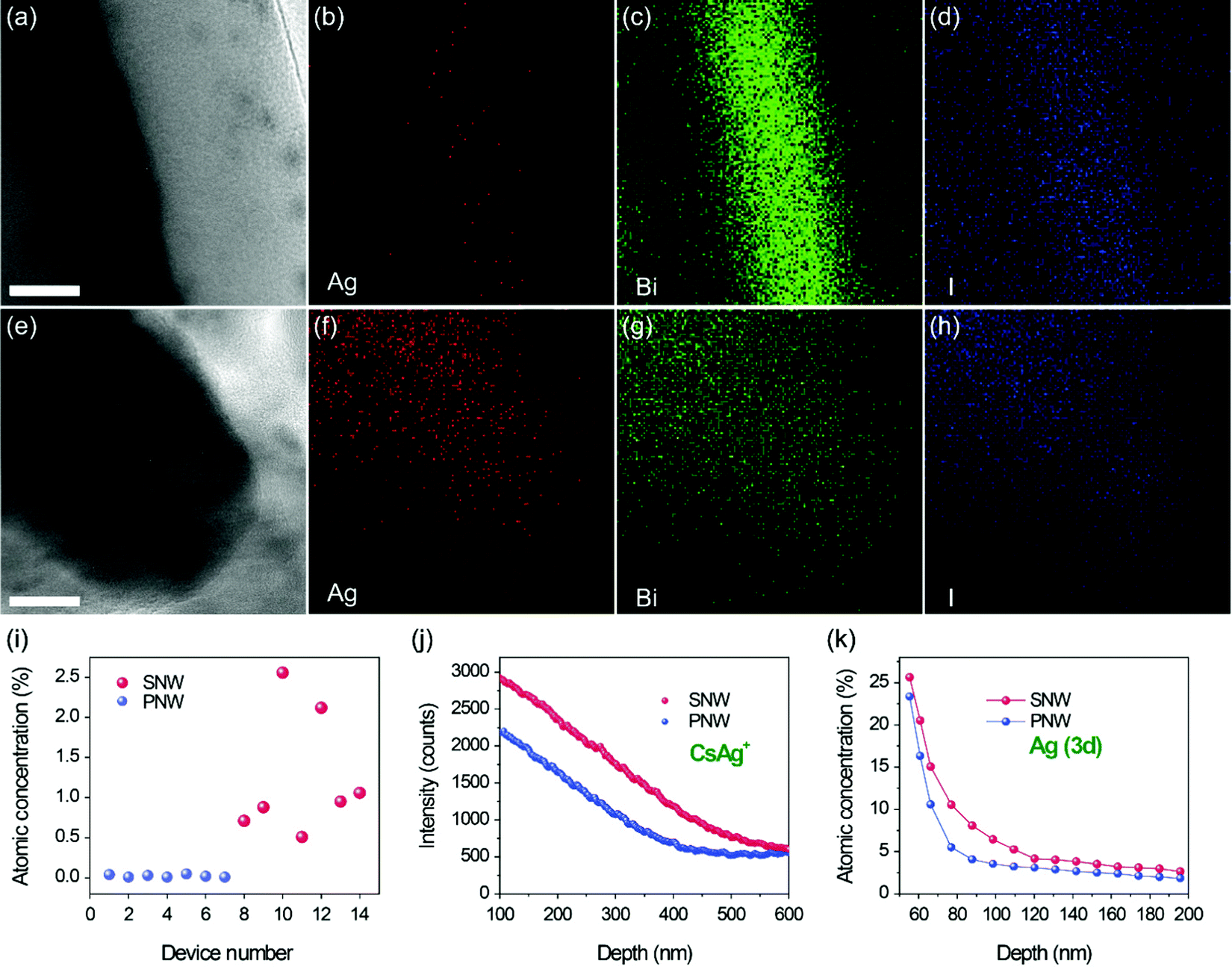 | ||
| Fig. 3 Mechanistic study of MBI NW Re-RAM. (a) TEM image of a PNW (scale bar: 20 nm). (b) EDS map of Ag in the PNW. (c) EDS map of Bi in the PNW. (d) EDS map of I in the PNW. (e) TEM image of a SNW (scale bar: 10 nm). (f) EDS map of Ag in the SNW. (g) EDS map of Bi in the SNW. (h) EDS map of I in the SNW. (i) Variation of Ag at concentration in MBI PNWs and SNWs. (j) Comparative ToF-SIMS depth profile of the PNW and SNW exhibiting a higher secondary CsAg+ ion intensity within the SNW. (k) Comparative XPS depth profile of the PNW and SNW exhibiting a higher Ag (3d) at. concentration in the SNW. | ||
Ballistic transport simulations and multilevel switching in MBI NW Re-RAM
In the case of an ECM Re-RAM the amount of injected Ag precisely determines the conductance state of the device which paves the way for computing and processing. Therefore, post empirical confirmation of Ag injection, in order to understand the impact of varying amounts of permeating Ag on the DOS and conductivity of the MBI NW Re-RAM, ballistic transport simulations were carried out. The mechanistic study presented in this work show that the conductance state of the switching layer is determined by closely distributed silver nanoclusters in the MBI material, and the formation, expansion, and connection of Ag nanoclusters are fundamentally equivalent to the Ag-doping of the MBI material. An atomistic structure of MBI is shown in Fig. 4a to model the atomic configuration in the region where the Ag filament is formed. Precisely the model is chosen such that it consists of 3 regions, namely, the left and right lead regions, and the center scattering region. Three Ag atoms were added to the lead regions to emulate the Ag reservoir; meanwhile, the formation of the Ag filament has been modelled in the scattering region by adding Ag atoms in this region. As the impact of Ag atom intrusion and its subsequent impact on the conductivity of the scattering region are of specific interest, the atom-projected DOS and the transmission coefficient of the scattering region have been calculated using first-principles. The DOS spectra of the scattering region with 0 Ag-atom, 1 Ag-atom, and 2 Ag-atoms in the MBI supercell are shown in Fig. 4b–d, respectively. It must be mentioned that the MBI structure without Ag atoms retained the semiconducting properties with its Fermi level positioned inside the energy band gap. In stark contrast, MBI structures with one or more Ag atoms developed metallic characteristics. In particular, the Fermi-level of the MBI structure with 2 Ag-atoms shifted deeper into the conduction band, which indicated a higher carrier concentration and consequently engendered conductivity.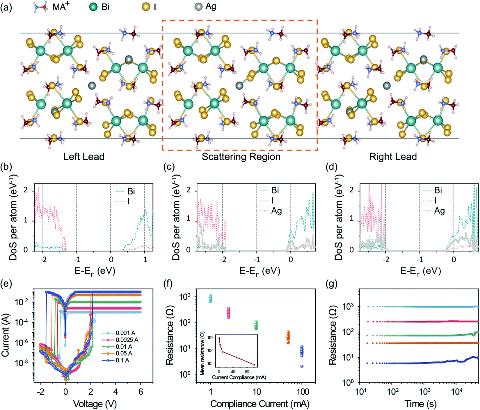 | ||
| Fig. 4 Ballistic transport simulations and multilevel switching in MBI NW Re-RAM. (a) Illustration showing the simulation structure with 3 components, namely, the left and right lead, and the center scattering region. All the 3 regions have the same structure of MA3Bi2I9 (MBI), each lead region has 3 Ag-atoms, and the scattering region possesses different numbers of Ag atoms. (b–d) The DoS spectra of the scattering region with 0 Ag-atom, 1 Ag-atom, and 2 Ag-atoms in the MBI supercell, respectively. (e) I–V characteristics of MBI NW Re-RAM with different operating compliances exhibiting multi-level switching. (f) LRS states of 15 different MBI NW Re-RAMs obtained by operating under different current compliances. (g) Plot showing temporal retention of multi-level LRSs in MBI NW Re-RAM. | ||
In a scenario, when the scattering region is much shorter than the mean free path, the scattering experienced by current carriers can be neglected, and Landauer's theory can be used to compute the conductivity of the scattering region under the ballistic transport mechanism.39 In the atomic structural model used in this work, the length of the scattering region is only about 1 nm, which not only mimics the possible distribution of Ag nanoclusters in the material structure, but also makes it reasonable to assume that the carrier scattering is negligible. Therefore, the transmission coefficient of the MBI scattering region with Ag atoms was also calculated using the Landauer–Buttiker formalism.40,41 The transmission coefficient T(E) versus energy spectrum is plotted in Fig. S9 of the ESI.† While comparing the T(E) for the different scenarios in the scattering region, it can be well observed that, post addition of Ag atoms in the scattering region, the T(E) rises drastically by several orders of magnitude. Despite the low calculation accuracy, which is limited by the computational power, the results of the transmission coefficient demonstrated a prominent trend that addition of Ag atoms to the MBI crystal structure can significantly increase the transmission probability. Following the Landauer–Buttiker formalism 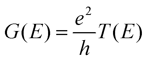 (where e is the electronic charge and h is Plank's constant), the enhanced transmission coefficient points to a higher conductance.40,41
The varying amounts of Ag inside the MBI NWs were precisely controlled, taking advantage of the multi-level switching behaviour of the device. As can be seen from Fig. 4e, five different compliance currents, namely 0.001 A, 0.0025 A, 0.01 A, 0.05 A and 0.1 A, were used for the standard I–V sweeps spanning the voltage range of 0 V → 6 V →−2 V →0 V. Fig. 4f shows the five distinct resistance states corresponding to the compliance induced LRS for a batch of 15 devices. It can be well noticed that the distinct resistance states showed no trace of overlap among each other indicating excellent data fidelity. Fig. 4g shows the temporal retention of the individual resistance states without any degradation for 5 × 10⁴ s. Fig. S10a and b of the ESI,† respectively, show the resistance spread and temporal retention of the states for thin-film MBI devices. The more obvious overlap among the resistance states, larger spread among the states for a fixed compliance in different devices and poorer retention (2.5 × 10³ s) are ascribed to the inferior material and electrical stability owing to the absence of the protective PAM in the thin film architecture. The single-crystallinity of the MBI NWs compared to the polycrystalline thin-film further helps in precise Ag injection and better control of the inflowing electrons upon application of different compliances, thereby contributing to the minimal overlap among the resistance states. Retention performance comparison among MBI NWs and MBI thin-films were also carried out as shown in Fig. S11 of the ESI.† The conductance state retention measurement at 105 °C for the NWs and thin-films proves beyond doubt the high temperature performance improvement in the NWs. The thin-film could only retain the LRS for 4000 s, whereas the NW device did not show any data degradation for 105 s. The excellent high temperature performance of the NW devices is ascribed to the higher thermal conductivity of the PAM compared to the perovskite NWs which assists with heat dissipation, thereby alleviating the chances of high temperature degradation which is usual for thin-film devices.
The multilevel switching behaviour could also be obtained with a pulsing measurement along with the compliance based technique as demonstrated in Fig. S12 (ESI†). The MBI NW devices exhibited programmability or modulation of the LRSs when fed with beyond threshold writing pulses possessing varying heights and widths. The LRSs were programmed more easily and precisely with less variation among the different devices while responding to pulse height rather than width, plausibly due to the greater dependence of the metallization process on the threshold electric field for switching which again is guided by the threshold switching voltage.
Image processing with MBI NW Re-RAM
To harness the multi-level analog signal processing capability of MBI NW Re-RAM devices, three kinds of image processing functions have been successfully demonstrated by 3 × 3 convolutional kernel image processing in this work.42,43 Kernel methods always require non-linear operations to achieve such functions, which are more complex with a flexible structure and are not suitable for memristor arrays. Nowadays, deep neural networks, using convolutional kernels as basic elements, requires highly power consuming platforms, such as graphics-processing units (GPUs). By implementing the convolution operation in a memristor array, a general application platform with lower power consumption and higher performance can be achieved. The input image chosen was that of a sundial clock as portrayed in Fig. 5a. The processed images by the MBI NW Re-RAM exhibiting embossing, outlining and sharpening are, respectively, shown in Fig. 5b–d. At the very outset, on-line training of the image processing was carried out and then the weights of the 3 × 3 convolutional kernel were mapped into the MBI NW Re-RAM with the aid of the transfer circuit provided in Fig. S13 of the ESI.† To circumvent the differential pair of a Re-RAM and an extra-peripheral circuit, the weight transfer circuit was chosen. The circuit design was capable of achieving both positive and negative neural weights with only one Re-RAM. It could also directly convert the input voltage to the output voltage in order to achieve matrix multiplication. The design of the MBI NW Re-RAM convolutional kernel was optimized to get as accurate resistance of the Re-RAM as possible. The details of the convolutional kernel process are provided in Fig. S14 (ESI†). The weights of the 3 × 3 convolutional kernels or the MBI NW Re-RAMs were restricted in the range of 10 Ω to 2 kΩ in order to obtain temporally robust resistance states. The individual states for each kernel corresponding to the embossing, outlining and sharpening are presented in Fig. 5e–g, respectively. The error bars of the resistance states represent the minimal variation of the states that were mapped for achieving the convolutional kernel for five cycles which also demonstrates the repeatability of the system. It must be mentioned here that the range of 10 Ω to 2 kΩ was chosen as a representative range and resistances outside this range within the ON/OFF ratio of the MBI NW devices can also be used in the convolutional kernel operation as depicted in Fig. S15 of the ESI.† The overall weight generation, updating and achievement of the convolutional kernels are provided in the form of a flow chart in Fig. S16 of the ESI.† To further prove the efficacy of our convolutional kernel general dataset images were also used besides the self-produced ones to demonstrate embossing, outlining and sharpening functions (see Fig. S17 of the ESI†).44 Also, an in-depth simulation and empirical study was carried out to ascertain the impact of resistance deviation, cell to cell and cycle to cycle variation of resistance states on the image processing performance. It was conclusively revealed that the image processing performance remained robust over a large range (−40% to 1000%) of resistance deviation and the cell to cell and cycle to cycle variations were within tolerable limits such that there was no significant impact on the embossing, outlining and sharpening functions. See Fig. S18–S22 of the ESI† for relevant discussion. As can be confirmed from Table 1, the first successful demonstration of image processing functions shown in Fig. 5 verified the computing capability of MBI NW Re-RAM and our proposed tuning method of multi-resistance states, which has the potential to eventually enable very large scale computing in more complex applications in conjunction with an advanced lithography based high density architecture in the future. Specifically, the PAM encapsulated MBI NWs with reliable image processing potency and minimal variation can be used to develop ultra-small Re-RAM cells with robust performance metrics in large scale cross-bar arrays to enable parallel read/write, speeding up the overall image processing task. In the future, there is also a scope for adopting a more on-chip processing approach with the MBI NWs, where the pulse mode of weight tuning with autonomous weight adaptation will lead to further improved image processing metrics in the form of lower power-consumption, faster overall processing and better accuracy.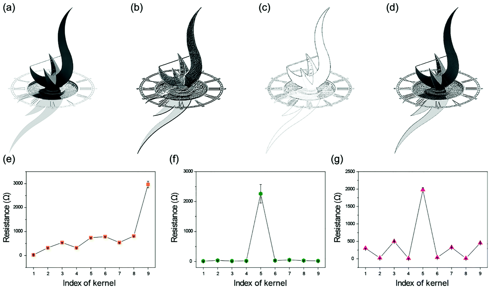 | ||
| Fig. 5 Image processing with MBI NW Re-RAM. (a) Image of the sundial that was fed as the input to the MBI NW Re-RAM for image processing. (b) Embossed sundial image obtained after processing by the MBI NW Re-RAM. (c) Outline of the sundial image obtained after processing by the MBI NW Re-RAM. (d) Sharpened sundial image obtained after processing by the MBI NW Re-RAM. (e–g) Resistance distribution of the MBI NW Re-RAMs, for five cycles, while performing the image processing tasks of embossing, outlining and sharpening. | ||
Conclusions
In order to alleviate the material and electrical stability limitations that prohibit HP thin-films to be deployed as switching layers in Re-RAMs for information processing and computing applications, MBI NWs rooted in a PAM were used as the switching matrix to implement the image processing task for the first time in this study. The MBI NW Re-RAM, thus designed, exhibited an ultra-fast switching speed of 2 ns (writing) and 900 ps (erasing), respectively, along with an excellent electrical endurance of 5 × 10⁶ cycles. The in-depth mechanistic study revealed Ag intrusion to be the triggering factor guiding the resistive switching. Bolstered by ballistic transport simulations and under different current compliances, the MBI NW Re-RAM showed multi-level switching with non-overlapping and temporally stable resistance levels. Utilizing compliance-controlled Ag injection in the monocrystalline MBI NWs, 3 × 3 convolutional kernels were designed which led to successful implementation of embossing, outlining and sharpening processing tasks. The MBI NW Re-RAM design and its associated study thus pave the way for HP perovskite Re-RAMs to be used for sophisticated computing and processing tasks in multi-functional electronic devices.Methods
Materials
Methyl ammonium iodide (MAI) powder was purchased from DYESOL.Device fabrication
Al chips with a 1.5 × 2 cm2 area were electro-polished and anodized in a 0.2 M oxalic acid solution overnight. The chips were further subjected to a second anodization step for 30 minutes, post an etching process in 6 wt% H3PO4 and 1.8 wt% CrO3 for 15 minutes at 98 °C, in order to form ordered PAM pores. The anodizing voltage used was 40 V. After using a voltage ramping down barrier thinning process, Bi clusters were electrodeposited to facilitate the VSSR perovskite NW growth, a process reported by us previously.30 In a closed tube with Ar flow, the VSSR process for 2 hours at 185 °C yielded highly ordered monocrystalline MBI NWs as the Bi reacted with the MAI powder generated vapor which acted as the precursor. Shadow masks with windows possessing an area of ∼1 mm2 were used for the deposition of the top electrode Ag which was thermally evaporated at a rate of 10 Å s−1. In the end, MBI NW Re-RAMs were packaged post wire-bonding, with an NOA81 UV-curable epoxy glue.Device characterization
The FIB cutting and SEM imaging of the MBI NW array was achieved using a Helios G4 UX FIB/FESEM system. The TEM study was performed using a JEM 2010 (JEOL) transmission electron microscopy system. The ToF-SIMS study was performed using a TOF SIMS V (ION-TOF GmbH) system. The XPS characterization was performed with a Kratos Axis Ultra DLD multi-technique surface analysis system. The XRD was performed with a Bruker D8 X-ray diffractometer. The PL characterization was done using an inVia (Renishaw) Micro Raman/Photoluminescence system.Ballistic transport simulations
The electronic structure was computed using the DFT equations that are implemented in the Quantum Espresso 6.3 code using plane waves as a basis set for the expansion of atomic orbitals and possessed periodic boundary conditions. Generalized gradient approximation (GGA) by Perdew–Burke–Ernzerhof (PBE) was considered for the exchange-correlation energy. The electron–ion interactions were described by means of nonlinear core-corrected ultra-soft (Vanderbilt) pseudo-potentials (USPP). In order to expand the Kohn–Sham (KS) orbitals, 500 Ry was used as the cutoff energy for the plane wave basis set, and 70 Ry was used for the cut-off kinetic energy. K-Points of 2 × 2 × 2 were used within the Monkhorst–Pack scheme for Brillouin zone integration. The zero-bias transmission spectrum was computed using the code PWCOND (a part of the Quantum-Espresso electronic structure package) via the Landauer–Buttiker formula with open boundary conditions comprising semi-infinite left and right leads bridged by the scattering region.Electrical measurements
The I–V, resistance state tuning and retention characterizations were performed with a Keithley 2450 source-meter and home-built LabVIEW programs. The device endurance was measured with an SG 300 potentiostat (Gamry Instruments). The switching speed pulses were produced using a Picosecond Pulse Labs Model 10070A pulse generator and the resistance levels were measured using a Keithley 2600 source-meter supported by home-built LabVIEW programs. The input pulses were measured with an ultra-fast DPO 70804C oscilloscope (maximum traceable voltage of 4.7 V). The multi-level pulsing measurements were performed with a Keithley 4200 SCS with a 4225 PMU and also a Keithley 2450 source-meter assisted with home-built LabVIEW programs. The electrical implementation of image processing was achieved using a National Instruments Controller PXI 8301, Multiplexer PXI 2530, SMU PXI 4130 and Keithley 2450 in conjunction.Author contributions
Z. Fan, S. Poddar and Y. Zhang conceptualized the experiments and analyzed the results. S. Poddar performed the device fabrication and detailed morphological and electrical characterizations. Y. Zhang performed the switching speed measurements and electrical implementation of image processing. Z. Chen performed the image processing simulations. Z. Ma performed the ballistic transport first-principles simulations. Y. Fu performed the XRD and PL characterizations. Y. Ding and C. L. J. Chan performed the schematic drawing and circuit design for image processing. Q. Zhang, D. Zhang and Z. Song helped with device fabrication and electrical characterizations. All authors participated in manuscript writing and articulation.Conflicts of interest
The are no conflicts of interest to declare.Acknowledgements
The authors thank Dr. Yuan Cai, Dr. Roy Ho, Prof. Lu Tao Weng and Mr. Nick KC Ho from Material and Characterization Preparation Facility (MCPF) at HKUST for technical assistance with FIB, TEM, SIMS and XPS characterizations. The authors also express their gratitude to the Center for 1D/2D Quantum Materials and State Key Laboratory of Advanced Displays and Optoelectronics Technologies at HKUST. The authors also thank Mr. Mitul Khanchandani for providing the image of the flower used in Fig. 1a to illustrate the concept flow of the study. The authors thank all the funders for their support. This work was financially supported by the General Research Fund (project no. 16205321, 16309018, and 16214619) from the Hong Kong Research Grant Council, Innovation Technology Commission Fund (project no. GHP/014/19SZ), Shenzhen Science and Technology Innovation Commission (project no. JCYJ20180306174923335 and JCYJ20170818114107730), Foshan Innovative and Entrepreneurial Research Team Program (2018IT100031), Guangdong Hong Kong-Macao Joint Laboratory for Intelligent Micro/Nano Optoelectronic Technology (project no. 2020B1212030010) and Zhongshan Municipal Science and Technology Bureau (ZSST21EG05).References
- H.-S. P. Wong and S. Salahuddin, Memory Leads the Way to Better Computing, Nat. Nanotechnol., 2015, 10, 191 CrossRef CAS PubMed.
- D. Ielmini and H.-S. P. Wong, In-memory Computing with Resistive Switching Devices, Nat. Electron., 2018, 1, 333–343 CrossRef.
- W. Zhang, B. Gao, J. Tang, P. Yao, S. Yu, M.-F. Chang, H.-J. Yoo, H. Qian and H. Wu, Neuro-inspired Computing Chips, Nat. Electron., 2020, 3, 371–382 CrossRef.
- D. Marković, A. Mizrahi, D. Querlioz and J. Grollier, Physics for Neuromorphic Computing, Nat. Rev. Phys., 2020, 2, 499–510 CrossRef.
- G. Indiveri, E. Linn and S. Ambrogio, Resistive Switching: From Fundamentals of Nanoionic Redox Processes to Memristive Device Applications, 2016, pp. 715–736 Search PubMed.
- H. L. Park, Y. Lee, N. Kim, D. G. Seo, G. T. Go and T. W. Lee, Flexible Neuromorphic Electronics for Computing, Soft Robotics, and Neuroprosthetics, Adv. Mater., 2020, 32, 1903558 CrossRef CAS PubMed.
- M. J. Yu, K. R. Son, A. C. Khot, D. Y. Kang, J. H. Sung, I. G. Jang, Y. D. Dange, T. D. Dongale and T. G. Kim, Three Musketeers: Demonstration of Multilevel Memory, Selector, and Synaptic Behaviors from an Ag-GeTe based Chalcogenide Material, J. Mater. Res. Technol., 2021, 15, 1984–1995 CrossRef CAS.
- A. C. Khot, T. D. Dongale, J. H. Park, A. V. Kesavan and T. G. Kim, Ti3C2-based MXene Oxide Nanosheets for Resistive Memory and Synaptic Learning Applications, ACS Appl. Mater. Interfaces, 2021, 13, 5216–5227 CrossRef CAS PubMed.
- T. D. Dongale, A. C. Khot, A. V. Takaloo and T. G. Kim, Facile Synthesis of Nickel Cobaltite Quasi-Hexagonal Nanosheets for Multilevel Resistive Switching and Synaptic Learning Applications, NPG Asia Mater., 2021, 13, 1–12 Search PubMed.
- X. Hong, D. J. Loy, P. A. Dananjaya, F. Tan, C. Ng and W. Lew, Oxide-based RRAM Materials for Neuromorphic Computing, J. Mater. Sci., 2018, 53, 8720–8746 CrossRef CAS.
- R. Islam, H. Li, P.-Y. Chen, W. Wan, H.-Y. Chen, B. Gao, H. Wu, S. Yu, K. Saraswat and H. P. Wong, Device and Materials Requirements for Neuromorphic Computing, J. Phys. D: Appl. Phys., 2019, 52, 113001 CrossRef.
- F. Ma, Y. Zhu, Z. Xu, Y. Liu, X. Zheng, S. Ju, Q. Li, Z. Ni, H. Hu and Y. Chai, Optoelectronic Perovskite Synapses for Neuromorphic Computing, Adv. Funct. Mater., 2020, 30, 1908901 CrossRef CAS.
- H. Tian, L. Zhao, X. Wang, Y.-W. Yeh, N. Yao, B. P. Rand and T.-L. Ren, Extremely Low Operating Current Resistive Memory based on Exfoliated 2D Perovskite Single Cystals for Neuromorphic Computing, ACS Nano, 2017, 11, 12247–12256 CrossRef CAS PubMed.
- Y. Zhu, L. Shu, Q. Zhang, Y. Zhu, S. Poddar, C. Wang, Z. He and Z. Fan, Moth Eye-inspired Highly Efficient, Robust, and Neutral-colored Semitransparent Perovskite Solar cells for Building-integrated Photovoltaics, EcoMat, 2021, 3(4), e12117 CAS.
- L. Gu, S. Poddar, Y. Lin, Z. Long, D. Zhang, Q. Zhang, L. Shu, X. Qiu, M. Kam and A. Javey, A Biomimetic Eye with a Hemispherical Perovskite Nanowire Array Retina, Nature, 2020, 581, 278–282 CrossRef CAS PubMed.
- Y. Wang, M. Zhang, K. Xiao, R. Lin, X. Luo, Q. Han and H. Tan, Recent Progress in Developing Efficient Monolithic All-perovskite Tandem Solar Cells, J. Semicond., 2020, 41, 051201 CrossRef CAS.
- G. Cao, C. Cheng, H. Zhang, H. Zhang, R. Chen, B. Huang, X. Yan, W. Pei and H. Chen, The Application of Halide Perovskites in Memristors, J. Semicond., 2020, 41, 051205 CrossRef CAS.
- S. I. Kim, Y. Lee, M. H. Park, G. T. Go, Y. H. Kim, W. Xu, H. D. Lee, H. Kim, D. G. Seo and W. Lee, Dimensionality Dependent Plasticity in Halide Perovskite Artificial Synapses for Neuromorphic Computing, Adv. Electron. Mater., 2019, 5, 1900008 CrossRef.
- B. Pradhan, S. Das, J. Li, F. Chowdhury, J. Cherusseri, D. Pandey, D. Dev, A. Krishnaprasad, E. Barrios and A. Towers, Ultrasensitive and Ultrathin Phototransistors and Photonic Synapses using Perovskite Quantum Dots Grown from Graphene Lattice, Sci. Adv., 2020, 6, eaay5225 CrossRef CAS PubMed.
- M. Kumar, H.-S. Kim, D. Y. Park, M. S. Jeong and J. Kim, Compliance-free Multileveled Resistive Switching in a Transparent 2D Perovskite for Neuromorphic Computing, ACS Appl. Mater. Interfaces, 2018, 10, 12768–12772 CrossRef CAS PubMed.
- C. C. Boyd, R. Cheacharoen, T. Leijtens and M. D. McGehee, Understanding Degradation Mechanisms and Improving Stability of Perovskite Photovoltaics, Chem. Rev., 2018, 119, 3418–3451 CrossRef PubMed.
- P. Toloueinia, H. Khassaf, A. Shirazi Amin, Z. M. Tobin, S. P. Alpay and S. L. Suib, Moisture-induced Structural Degradation in Methylammonium Lead Iodide Perovskite Thin Films, ACS Appl. Energy Mater., 2020, 3, 8240–8248 CrossRef CAS.
- Q. Wang, B. Chen, Y. Liu, Y. Deng, Y. Bai, Q. Dong and J. Huang, Scaling Behavior of Moisture-induced Grain Degradation in Polycrystalline Hybrid Perovskite Thin Films, Energy Environ. Sci., 2017, 10, 516–522 RSC.
- S. Chen and J. Huang, Recent Advances in Synaptic Devices Based on Halide Perovskite, ACS Appl. Electron. Mater., 2020, 2, 1815–1825 CrossRef CAS.
- Q. Zhang, D. Zhang, L. Gu, K.-H. Tsui, S. Poddar, Y. Fu, L. Shu and Z. Fan, Three-dimensional Perovskite Nanophotonic Wire Array-based Light-emitting Diodes with Significantly Improved Efficiency and Stability, ACS Nano, 2020, 14, 1577–1585 CrossRef CAS PubMed.
- D. Zhang, L. Gu, Q. Zhang, Y. Lin, D.-H. Lien, M. Kam, S. Poddar, E. C. Garnett, A. Javey and Z. Fan, Increasing Photoluminescence Quantum yield by Nanophotonic Design of Quantum-confined Halide Perovskite Nanowire Arrays, Nano Lett., 2019, 19, 2850–2857 CrossRef CAS PubMed.
- A. Waleed and Z. Fan, Fabrication of Stable Organometallic Halide Perovskite NWs based Optoelectronic Devices, Sci. Bull., 2017, 62, 645–647 CrossRef CAS.
- S. Poddar, Y. Zhang, L. Gu, D. Zhang, Q. Zhang, S. Yan, M. Kam, S. Zhang, Z. Song and W. Hu, Down-Scalable and Ultra-fast Memristors with Ultra-high Density Three-Dimensional Arrays of Perovskite Quantum Wires, Nano Lett., 2021, 21(12), 5036–5044 CrossRef CAS PubMed.
- Y. Zhang, S. Poddar, H. Huang, L. Gu, Q. Zhang, Y. Zhou, S. Yan, S. Zhang, Z. Song and B. Huang, Three-dimensional Perovskite Nanowire Array–based Ultrafast Resistive RAM with Ultralong Data Retention, Sci. Adv., 2021, 7, eabg3788 CrossRef CAS PubMed.
- L. Gu, M. M. Tavakoli, D. Zhang, Q. Zhang, A. Waleed, Y. Xiao, K. H. Tsui, Y. Lin, L. Liao and J. Wang, 3D Arrays of 1024-pixel Image Sensors Based on Lead Halide Perovskite Nanowires, Adv. Mater., 2016, 28, 9713–9721 CrossRef CAS PubMed.
- S. Poddar, Y. Zhang, Y. Zhu, Q. Zhang and Z. Fan, Optically Tunable Ultra-fast Resistive Switching in Lead-free Methyl-ammonium Bismuth Iodide Perovskite Films, Nanoscale, 2021, 13, 6184–6191 RSC.
- R. Li, X. Xu, B. Zhu, X.-Y. Li, Y. Ning, R. Mu, P. Du, M. Li, H. Wang and J. Liang, In situ Identification of the Metallic State of Ag Nanoclusters in Oxidative Dispersion, Nat. Commun., 2021, 12, 1–9 CrossRef PubMed.
- J. L. Gottfried, D. K. Smith, C.-C. Wu and M. L. Pantoya, Improving the explosive performance of aluminum nanoparticles with aluminum iodate hexahydrate (AIH), Sci. Rep., 2018, 8, 1–12 CAS.
- B. Weng, X. Zhang, N. Zhang, Z.-R. Tang and Y.-J. Xu, Two-dimensional MoS2 Nanosheet-coated Bi2S3 Discoids: Synthesis, Formation Mechanism, and Photocatalytic Application, Langmuir, 2015, 31, 4314–4322 CrossRef CAS PubMed.
- X. Zhu, J. Lee and W. D. Lu, Iodine Vacancy Redistribution in Organic–inorganic Halide Perovskite Films and Resistive Switching Effects, Adv. Mater., 2017, 29, 1700527 CrossRef PubMed.
- K. Luo, T. Clair, X. Lai and D. Goodman, Silver Growth on TiO2 (110)(1× 1) and (1× 2), J. Phys. Chem. B, 2000, 104, 3050–3057 CrossRef CAS.
- B.-H. Mao, R. Chang, L. Shi, Q.-Q. Zhuo, S. Rani, X.-S. Liu, E. C. Tyo, S. Vajda, S.-D. Wang and Z. Liu, A Near Ambient Pressure XPS Study of Subnanometer Silver Clusters on Al2O3 and TiO2 Ultrathin Film Supports, Phys. Chem. Chem. Phys., 2014, 16, 26645–26652 RSC.
- G. Moretti, The Wagner Plot and the Auger Parameter as Tools to Separate Initial-and Final-state Contributions in X-ray Photoemission Spectroscopy, Surf. Sci., 2013, 618, 3–11 CrossRef CAS.
- C. W. J. Beenakar and H. van Houten, Quantum Transport in Semiconductor Nanostructures in Solid State Physics, Academic Press., 1991, vol. 44, pp. 1–228 Search PubMed.
- S. Datta, Electronic Transport in Mesoscopic Systems, Cambridge University Press, 1997 Search PubMed.
- A. Smogunov, A. Dal Corso and E. Tosatti, Ballistic Conductance of Magnetic Co and Ni Nanowires with Ultrasoft Pseudopotentials, Phys. Rev., 2004, 70, 045417 Search PubMed.
- H. Yeon, P. Lin, C. Choi, S. H. Tan, Y. Park, D. Lee, J. Lee, F. Xu, B. Gao and H. Wu, Alloying Conducting Channels for Reliable Neuromorphic Computing, Nat. Nanotechnol., 2020, 15, 574–579 CrossRef CAS PubMed.
- E. Giacomin, T. Greenberg-Toledo, S. Kvatinsky and P.-E. Gaillardon, A Robust Digital Rram-based Convolutional Block for Low-Power Image Processing and Learning Applications, IEEE TCAS-I, 2018, 66, 643–654 Search PubMed.
- J. Deng, W. Dong, R. Socher, L.-J. Li, K. Li and F.-F. Li, ImageNet: A Large-scale Hierarchical Image Database, Proc. IEEE Comput. Soc. Conf. Comput. Vis. Recognit., 2009, pp. 248–255 Search PubMed.
- B. Hwang and J.-S. Lee, Lead-free, Lead-free, Air-stable Hybrid Organic–inorganic Perovskite Resistive Switching Memory with Ultrafast Switching and Multilevel Data Storage, Nanoscale, 2018, 10, 8578–8584 RSC.
- B. Hwang and J.-S. Lee, Hybrid Organic-inorganic Perovskite Memory with Long-term stability in Air, Sci. Rep., 2017, 7, 1–7 CrossRef CAS PubMed.
- R. A. John, N. Yantara, Y. F. Ng, G. Narasimman, E. Mosconi, D. Meggiolaro, M. R. Kulkarni, P. K. Gopalakrishnan, C. A. Nguyen and F. De, Angelis, Ionotronic Halide Perovskite Drift-diffusive Synapses for Low-power Neuromorphic Computation, Adv. Mater., 2018, 30, 1805454 CrossRef PubMed.
- R. Wang, P. Chen, D. Hao, J. Zhang, Q. Shi, D. Liu, L. Li, L. Xiong, J. Zhou and J. Huang, Artificial Synapses Based on Lead-Free Perovskite Floating-Gate Organic Field-Effect Transistors for Supervised and Unsupervised Learning, ACS Appl. Mater. Interfaces, 2021, 13, 43144–43154 CrossRef CAS PubMed.
Footnotes |
| † Electronic supplementary information (ESI) available. See DOI: https://doi.org/10.1039/d2nh00183g |
| ‡ These authors contributed equally to this work. |
| This journal is © The Royal Society of Chemistry 2022 |