
Inkjet printing of two-dimensional van der Waals materials: a new route towards emerging electronic device applications
Kyungjune
Cho
*a,
Takhee
Lee
 b and
Seungjun
Chung
*ac
b and
Seungjun
Chung
*ac
aSoft Hybrid Materials Research Center, Korea Institute of Science and Technology, Seoul 02792, Korea. E-mail: kcho@kist.re.kr; seungjun@kist.re.kr
bDepartment of Physics and Astronomy, and Institute of Applied Physics, Seoul National University, Seoul 08826, Korea
cKHU-KIST Department of Converging Science and Technology, Kyung Hee University, Seoul, 02447, Korea
First published on 20th July 2022
Abstract
Two-dimensional (2D) van der Waals (vdW) materials are considered one of the most promising candidates to realize emerging electrical applications. Although until recently, much effort has been dedicated to demonstrating high-performance single 2D vdW devices, associated with rapid progress in 2D vdW materials, demands for their large-scale practical applications have noticeably increased from a manufacturing perspective. Drop-on-demand inkjet printing can be the most feasible solution by exploiting the advantages of layered 2D contacts and advanced 2D vdW ink formulations. This review presents recent achievements in inkjet-printed 2D vdW material-based device applications. A brief introduction to 2D vdW materials and inkjet printing principles, followed by various ink formulation methods, is first presented. Then, the state-of-the-art inkjet-printed 2D vdW device applications and their remaining technical issues are highlighted. Finally, prospects and challenges to be overcome to demonstrate fully inkjet-printed, high-performance 2D vdW devices are also discussed.
 Kyungjune Cho | Kyungjune Cho received his PhD degree from the Department of Physics and Astronomy, Seoul National University in 2019, and then he was a postdoctoral researcher at the Department of Nano-systems from Ions, Spins and Electrons, Max Planck Institute of Microstructure Physics, Halle, Germany, until 2021. He is now a postdoctoral researcher at the Korea Institute of Science and Technology (KIST), Seoul, Republic of Korea. His current research interests include emerging low-dimensional materials and their interfaces. He has been highly productive during his career with over 50 research publications. |
 Takhee Lee | Takhee Lee is a Professor in the Department of Physics and Astronomy, Seoul National University, Korea. He received his BS and MS degree in physics at Seoul National University in 1992 and 1994, respectively, and he received his PhD degree in physics at Purdue University, USA, in 2000. He was a postdoctor at Yale University, USA until 2004. His current research interests are characterization of the electrical properties of structures involving molecular self-assembled monolayers, polymers, semiconductor nanomaterials, and their assembly into electronic devices. He edited 2 books and wrote 11 book chapters, 18 review articles, and more than 300 journal articles. |
 Seungjun Chung | Seungjun Chung received his PhD degree from the Department of Electrical Engineering and Computer Science, Seoul National University in 2012, and then he was a postdoctoral researcher at the Department of Electrical Engineering and Computer Sciences, University of California, Berkeley until 2016. He is now a principal research scientist at the Korea Institute of Science and Technology (KIST), Seoul, Republic of Korea. His current research interests include additive manufacturing for advanced stretchable electronics and emerging low-dimensional semiconductor devices. He has been highly productive during his career with over 80 research publications, and 40 domestic and foreign Patents. |
Introduction
The upcoming “Internet of Everything”, which will enable our surrounding electronics to be closely interconnected, has accelerated the development of next-generation electronics based on emerging materials.1–5 In recent years, two-dimensional (2D) van der Waals (vdW) materials have been regarded as one of the most promising candidates owing to their superior properties, including electrical, optical, and even mechanical characteristics. Specifically, their inherently different electrical and optoelectronic behaviours when thinned down to the atomic limit by exploiting either physical or chemical exfoliation methods have attracted significant attention from both research and industrial societies. In addition to well-known pioneering materials in the field of 2D vdW materials, e.g., graphene (Gr) and semiconducting transition metal dichalcogenides (TMDs), various novel vdW materials have been discovered, which can be used as superconductors, ferro- and antiferromagnets, topological insulators, and Weyl semimetals.6–17Notably, their recent advances to realize practical applications have been encouraged beyond single device demonstration, initiating vibrant research for cost-effective, large-area, and high-yield mass production. In this sense, omnipresent inkjet printing has been employed as a feasible solution to meet the aforementioned demands of large area, low cost, easy processability, and high compatibility. In addition, inkjet printing can offer a high degree of design freedom for 2D nanoelectronics while maintaining their high electrical performance.18–26 2D vdW material-based inks are also suitable for use in inkjet printing as active pigments due to the rapid progress in the ink formulation methodology from synthesis of 2D vdW materials to novel electrochemical exfoliation methods. Moreover, inkjet printing of 2D vdW layered nanosheet pigments has attractive advantages in layer-by-layer stacking from the device performance perspective over other materials such as zero-dimensional (0D) quantum dots and one-dimensional (1D) nanowires.27–29 To create transport channels for active layers, for instance, electrodes and semiconducting channels, the printed low-dimensional nanocomposites must be interconnected with neighbouring dots/wires/sheets to transport charge carriers. When nanocomposites are interconnected, energy barriers are inevitably formed at the contact regions; therefore, tackling such inherent contacts is significantly important to improve the charge transport properties. As depicted in Fig. 1a, 0D quantum dot-based nanocomposites form point contacts, resulting in high energy barriers. From a mesoscopic perspective, the size of the 0D system also gives rise to a large number of point contacts, resulting in high channel resistance. For 1D nanocomposite channels, although there would also be high energy barriers from point contacts among wires, higher conductivity compared to 0D systems can be delivered, which would be coupled with a lower number of point contacts (Fig. 1b). Interestingly, 2D nanocomposites have shown the possibility of achieving much higher conductivity, creating 2D contacts connected layer-by-layer due to the capillary force between neighbouring sheets corresponding to much lower energy barriers, as shown in Fig. 1c. Although matured inkjet-printed 1D nanowire (NW)-based devices have shown better overall electronic performances as of now,30 it has been believed that inkjet-printed 2D electronics have a huge potential owing to their intrinsic advantages over 1D and 0D films, such as higher surface coverage, lower barrier density, and lower barrier height from their structural nature. Moreover, manufacturing heterostructures of 2D materials with varying material combinations, thicknesses, and structures are also feasible.27 Therefore, for emerging inkjet-printed devices with low-dimensional materials, 2D layered nanosheets are the most favourable for demonstrating a well-stacked channel via drop-on-demand deposition without complicated alignment processing (Fig. 1d). Note that alignment techniques, e.g., shear rolling, have been widely employed in 1D nanowire systems for better electrical performance. Utilizing these advantages, various inkjet-printed 2D vdW material-based emerging devices, such as sensors, photodetectors, thermoelectrics, wearable electronics, and even superconducting devices, have been vigorously investigated.5,18,21,22,31–44 In this regard, many researchers have reported noteworthy results in novel ink formulation methods and inkjet-printed emerging device applications over the last decade. Representatively, Kelly et al. reported all-inkjet-printed thin-film transistors (TFTs) with layered 2D Gr, WSe2, and boron nitride (BN) as an electrode, a semiconductor, and insulating layers, respectively (Fig. 1e).45
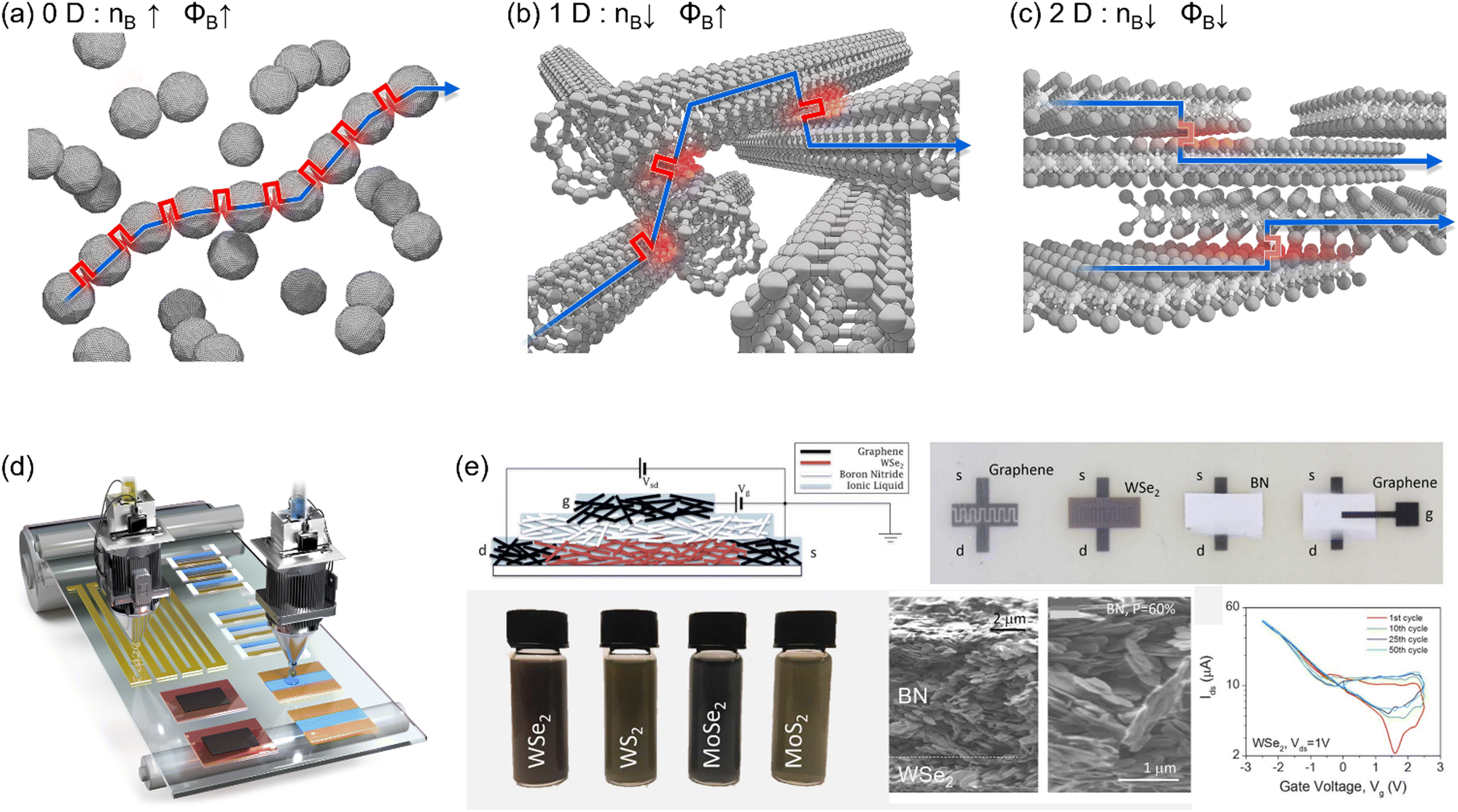 | ||
| Fig. 1 (a) The conducting path through connected 0D nanoparticles includes a large number of point contacts with neighbouring nanoparticles, with high energy barriers. (b) The conducting path through 1D nanowires includes a dramatically reduced number of point contacts with high energy barriers. (c) The conducting path through 2D nanosheets includes a greatly reduced number of sheet contacts with also greatly reduced the energy barrier due to the large contact area. (d) Schematic image of the fabrication of various electronic devices by using inkjet printing. (e) 2D vdW inks, fully printed vdW-based field-effect transistor and its transfer curves. Reproduced with permission.45 Copyright 2017, Publisher AAAS. | ||
This minireview highlights recent achievements in inkjet-printed 2D vdW material-based devices from conventional TFTs to the most recently reported Josephson junction device. The overarching aim is to show the feasibility of realizing emerging 2D layered devices associated with inkjet printing and provide an overview of recent efforts to improve their electrical performance. We hereby assume that the time is right to summarize the progress in inkjet printing of 2D vdW materials, especially from the perspective of 2D ink preparation with a suitable inkjet printing strategy, and the state-of-the-art device applications in line with the latest trends in 2D electronics.
2D vdW ink formulation methods
Pigments: representative 2D vdW materials
To establish an inkjet printing strategy, the formulation of a rheologically well-designed ink is the starting point. Before discussing the rheological principles and methodology for ink formulation, we first focus on the 2D vdW material pigments. As the 2D vdW family has been intensively investigated due to its attractive properties, remarkable developments in the field of vdW material synthesis from bulk crystals to large-area monolayers have also been achieved. In particular, conventional synthesis methods, e.g., molecular beam epitaxy (MBE), and chemical vapour deposition (CVD), have enabled the synthesis of large-area monolayers comparable to high-quality bulk crystals synthesized by chemical vapour transport (CVT).6,7,31,46–51 Owing to these continued efforts and progress, a variety of large-area synthesized 2D vdW materials now exhibit attractive physical properties. In addition to representative semimetallic Gr, insulating hexagonal BN (h-BN), semiconducting TMDs (e.g., MoS2 and WSe2), and metallic TiS2, we now have magnetic (CrI3, CrCl3, CrBr3, Fe3GeTe2, etc.) and even superconducting (NbSe2 and Bi2Te3) vdW materials.52–62 In particular, their layer-dependent energy band structures and the feasibility of fabricating clean heterostructures without lattice mismatch concerns accelerate the progress in exploring both in-depth material characteristics and optimized device fabrication.11,52,53,63,64The energy band structure of a 2D vdW material is tuneable by adjusting prominent parameters, such as the number of layers.65 Additionally, even the stacking angles of a heterostructure were found to possibly act as a key factor in modulating the band structure since they can introduce an additional periodic potential to the system by forming a moiré lattice.66–68 Additional functionalities, e.g., superconductivity of Gr68 or ferroelectricity of twisted h-BN,66 can also be delivered by introducing the vdW transfer technique. The absence of dangling bonds on the surface of 2D vdW materials and their weak vdW interactions between layers provide promising opportunities to fabricate heterostructures with atomically clean interfaces with different neighbouring 2D layers. With these advantages, atomically clean heterostructures with a variety of vdW material combinations can be realized by employing advanced fabrication methodologies, such as the polydimethylsiloxane (PDMS)-based vdW dry transfer method.69 For example, insulating h-BN can be used to encapsulate underlying air-sensitive 2D materials, and Gr can be used as a contact to enhance the charge injection due to its high conductivity and low density of states near the Fermi level.52,53 In particular, owing to the rapid progress in the vdW transfer technique, the field of twistronics has been opened. As a result, superconducting 1.1° twisted bilayer Gr has become the most well-known twisted homobilayer system, also called “magic-angle” Gr.67 These 2D vdW heterostructures have been widely studied in a variety of research fields, not only limited to electronics but also including thermoelectrics, magnetism, spintronics, and topology.9,12,50,70–77
From the 2D vdW material perspective, much effort has been dedicated to synthesizing and discovering new vdW materials exhibiting various electrical properties, as shown in Fig. 2. For example, although magnetism is one of the most important natures, in-depth research begun relatively recently due to the limited intrinsically magnetic vdW materials. As a result of continued efforts to find and synthesize magnetic vdW materials, studies on magnetism-related research including spintronics of 2D magnetic vdW materials have been initiated.9,49,56,58,76,78,79 In addition, the 2D heterostructure platform has a strong advantage without the lattice mismatch concern, while fabricating magnetic heterostructures by using conventional magnetic materials and device fabrication is difficult due to lattice distortion, which can also distort the magnetic dipole alignment. Similarly, research on 2D topological insulators and Weyl semimetals has begun, as they have recently discovered.62,75–77
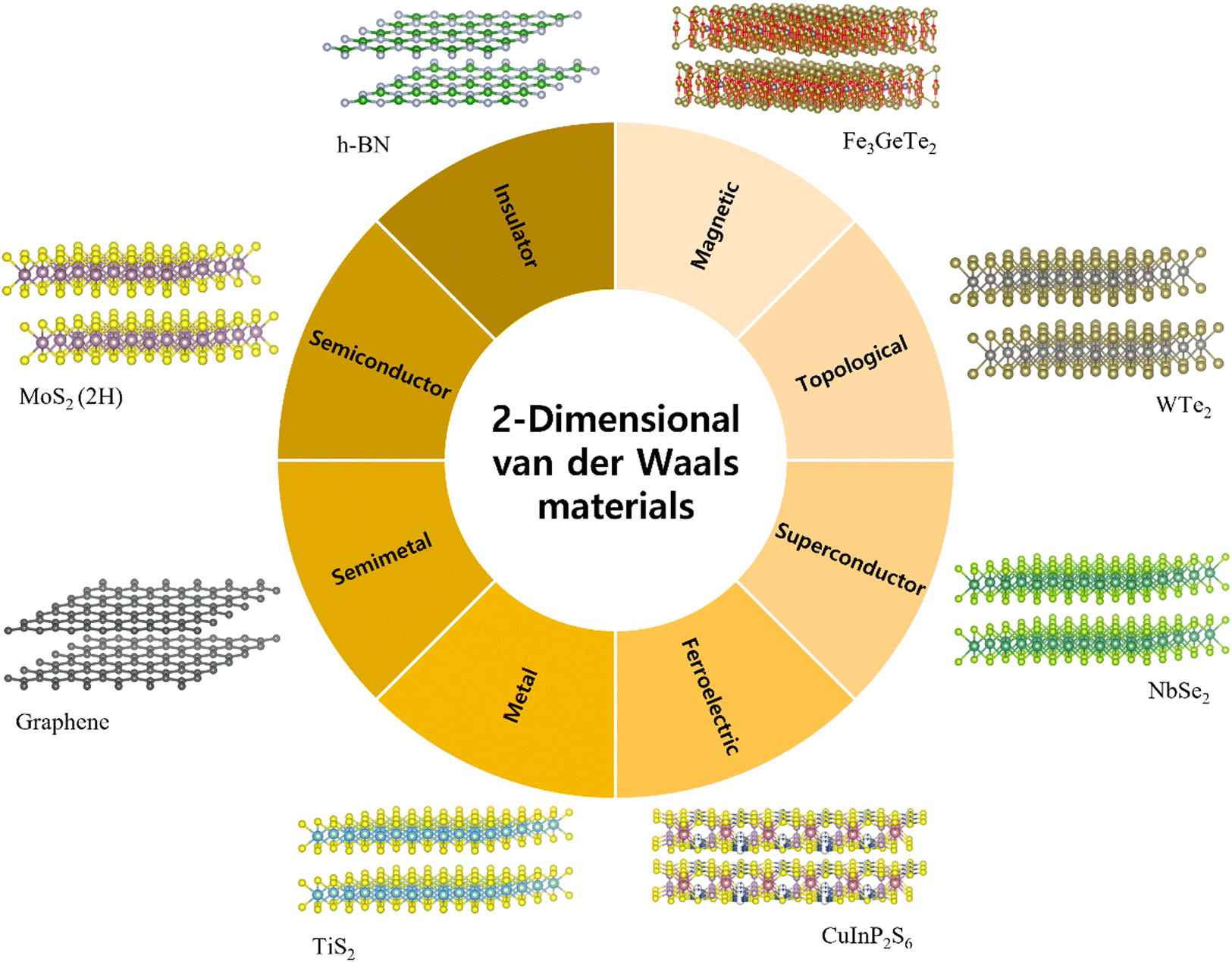 | ||
| Fig. 2 Schematic illustration of functional 2D vdW materials. | ||
However, the results of these emerging materials are still limited to a single device fabricated by using mechanical exfoliation methods, which are not suitable for practical applications. Due to the strong motivation for transitioning from proof-of-concept to large-scale application, drop-on-demand inkjet printing has become a strong candidate from a manufacturing perspective because it offers high resolution, less material waste, and a wide range of substrate compatibility as well as noncontact and maskless processability. Specifically, layer-by-layer contacts of 2D vdW materials can be facilely demonstrated by using inkjet printing, which can presumably create a significant synergistic effect with the advantages of 2D vdW materials.21,24,26 In this frame, significant efforts have been devoted to adapting 2D vdW materials to inkjet printing to meet these demands and extend the boundaries of technologies.
Principles of 2D vdW ink formulation and inkjet printing
Therefore, high-quality bulk crystals of 2D materials have been widely grown via CVT prior to exfoliation.6,7,49,51 As illustrated in Fig. 3a, CVT generally uses two temperature zones in a vacuum-sealed ampul: (1) a hot zone where the source materials are placed and (2) a cool zone where the synthesized bulk crystals are deposited after the chemical reaction (note that they can be reversed if the chemical reaction for synthesis is endothermic). After the synthesis process, the deposited bulk crystals are removed from the ampul and placed on an electrode (anode or cathode) in an ionic liquid solvent for the next step, electrochemical exfoliation. This involves exfoliation from a wide range of 2D vdW bulk crystals induced by the external energy, such as mechanical energy from ultrasonication, or driven by an electrochemical reaction in a target solvent. LPE can be utilized to produce a wide range of 2D vdW material-based inks.81,82 In detail, the weak layer-by-layer interaction can be easily broken by the introduction of external stress, intercalation of ions between layers, or creation of bubbles through chemical reactions of intercalated ions, resulting in isolated free-standing mono- or few layers in the target solvents.
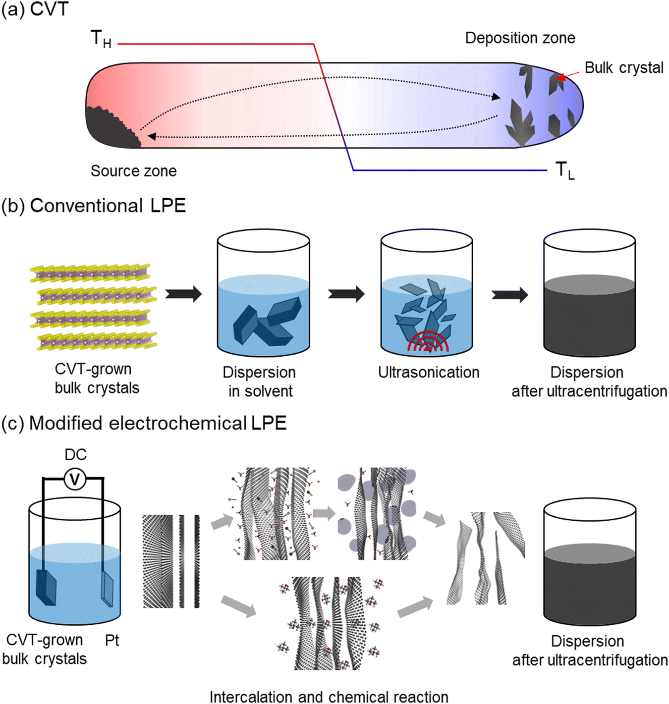 | ||
| Fig. 3 (a) Schematic illustration of the CVT synthesis method with two different temperature zones. The source materials heated in the hot zone are transported as a gas phase, depositing in the cool zone as a crystal phase. (b) Schematic illustration of the LPE method. (c) Schematic illustration of the electrochemically assisted LPE method. The electrochemical exfoliation generally involves ion intercalation inducing delamination. | ||
At the early stage of the LPE method, as illustrated in Fig. 3b, the bulk crystal pieces are just placed in the solvent, followed by ultrasonication to promote exfoliation in the liquid. Then, the 2D vdW material dispersed in the solvent is generally subjected to multiple centrifugations to selectively collect free-standing layers with a target thickness or size. Importantly, because the condition of the applied external force, e.g., the strength of the ultrasonication wave or the exposure time, can determine the average size of free-standing flakes, corresponding to the quality of 2D flakes, it should be carefully optimized to prevent their severe destruction. In addition, after the exfoliation process, the delaminated 2D flakes can aggregate.
To overcome these hurdles, additional processes have been proposed, for example, the aforementioned electrochemical reactions or ion intercalations. The electrochemical exfoliation strategy entails an external voltage bias along with ionic solvents that have ion intercalants in them so that ions can migrate from the solvent to the electrode where the bulk crystal is located.83–88 Consequently, the ions intercalate into the gaps between the layers of the bulk crystal, as shown in Fig. 3c. In summary, the intercalated ions located between the layers broaden the interlayer distance, weakening the weak vdW interaction and thus promoting delamination. Sometimes, air bubbles are intentionally produced between the layers as byproducts of induced electrochemical reactions during the chemical reactions. Such chemically created air bubbles grow larger as the chemical reaction continuously progresses. Eventually, they physically push away neighbouring layers, stimulating delamination of bulk crystals. Note that the bulk crystal can be placed on either the anode side or cathode side depending on the intercalants (i.e., positive ions or negative ions) used for exfoliation. These should be carefully determined depending on the purposes because ionic intercalants often introduce additional defects to the 2D vdW crystals or promote unwanted oxidation and lattice distortions.89 In addition, intercalated ions can prevent potential aggregation without additives. These methods generally require milder ultrasonication than in conventional LPE because the vdW interactions between the layers are already weakened by ions and bubbles or often do not require ultrasonication at all. Then, centrifugation can be performed for dispersion purposes. Therefore, these approaches promise a higher chance of producing large-area, less-defective high-quality flakes in 2D vdW inks, which can lead to a higher electronic performance of printed devices.
Inkjet printing of 2D vdW inks
Drop-on-demand (DOD) inkjet printing can eject out 2D vdW inks from nozzles to underlying layers, so it is one of the most promising candidates for direct film deposition without a complicated etching process. There are two representative types of printing systems, which have a nozzle based on (a) a piezoelectric actuator or (b) a thermal heater to form ink droplets and drive the jetting force, as illustrated in Fig. 4a.90–92 In the case of inkjetting by a piezoelectric actuator, extrinsic voltage pulses are applied to the piezoelectric transducer located in the nozzle, and in turn, the moving membrane of the transducer creates pressure pulses that are applied to the ink inside the nozzle. Likewise, air bubbles can be created by Joule heating from thermal nozzles, and the evaporated gas also forms ink droplets and creates pressure for jetting. However, in the latter case, the range of the solvent is limited because the ink solution should be volatile to reliably create the desired size of bubbles. Therefore, water or short-chain alcohols are typically considered ink solvents for thermal actuator systems, while a wide range of solvents can be employed in piezoelectric actuator systems. In addition, the ink ejection in response to the pressure generated by the piezoelectric element can allow relatively good resolution, requiring lower temperature compared to the thermal counterpart, which suffers from ink degradation concerns and temperature-sensitive solvent choice. For these reasons, piezoelectric nozzles are more frequently adopted for state-of-the-art emerging applications using DOD inkjet printing.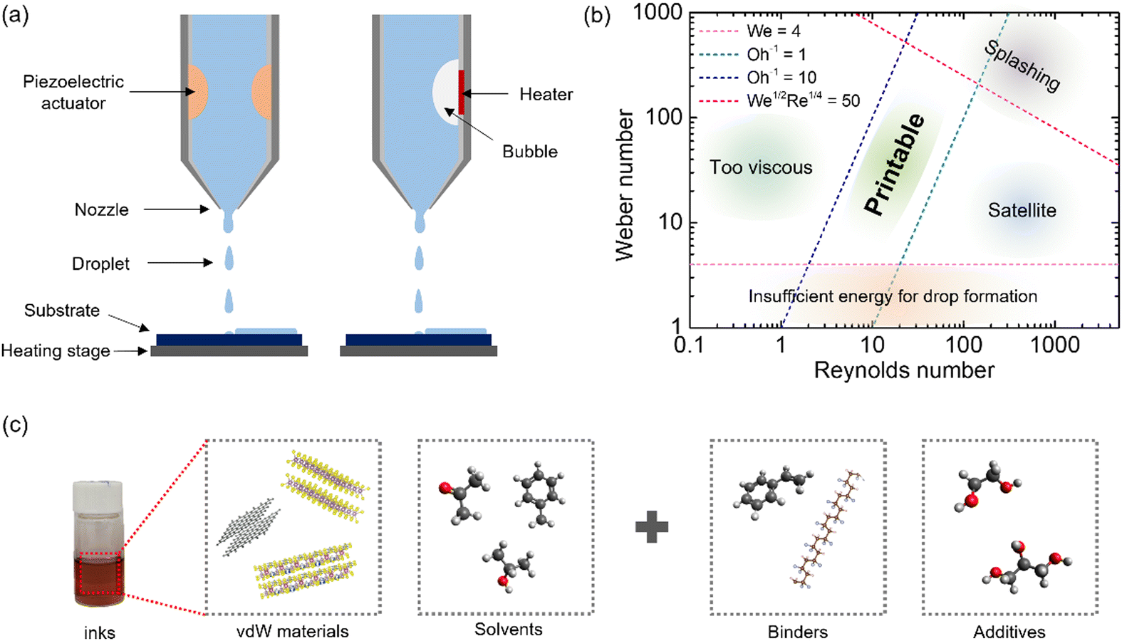 | ||
| Fig. 4 (a) Two representative types of nozzles for inkjet printing with different actuators: a piezoelectric transducer and a heater. (b) Rheological parameters and expected printability. (c) General compositions of 2D vdW inks. | ||
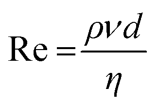
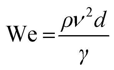
To pursue the best printing quality, the rheology of the ink must also be delicately controlled since the rheological properties of inks play a central role in DOD inkjet printing. In other words, the interfacial properties and rheological parameters of 2D vdW inks, such as density, surface tension, and viscosity, should be carefully considered to promote high-quality printed layers. According to previous studies, the following conditions are empirically required for a well-formulated ink that is good in terms of stability and printability. First, to avoid nozzle clogging, the average size of dispersed pigments, the vdW nanoflakes, should be less than 1/50 of the nozzle diameter.33,93 Additionally, the viscosity dominantly influences the microfluidic dynamics of the ink droplets. For example, if the viscosity is too high, then the ink droplets will not be easily ejected from the nozzle. In contrast, if the viscosity is too low, then the droplet will not be stabilized and consequentially form satellite drops. For these reasons, the suitable viscosity range is known to be 1–25 mPa s−1. Similarly, 20–50 mN m−1 surface tension has been suggested to avoid difficulties in inkjetting from nozzles. Owing to prolonged efforts, these rheological parameters have been merged into two dimensionless numbers, the Reynolds number (Re), which is known to predict flow patterns, and the Weber number (We), which is used to analyse fluid flows, written as follows:
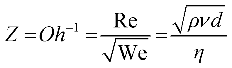
where ρ is the density and v is the velocity of the jetted ink, d is the diameter of the nozzle, η is the viscosity of the ink, and γ is the ink surface tension.94,95 These two numbers have been known to account for the formation of droplets. Note that such conditions and numbers have been found empirically and cannot be an absolute criterion. Likewise, when the velocity is too low and the surface tension is too high such that the droplet cannot overcome the surface tension barrier (We < 4), droplets would not be formed in flight. In addition, to precisely predict the quality of inkjetting, another dimensionless number Z, the inverse of the Ohnesorge number (Oh = We1/2/Re),
has been generally employed. Note that Z does not require the fluid velocity; thus, it can only explain the physical properties of the fluid and the characteristic length.94 According to previous studies, the suitable range of Z values to avoid poor inkjettability, e.g., not ejecting or forming satellite droplets, is approximately 1 to 10.97
As we discussed, since the quality of inkjetting affects the quality of printed features, not only exfoliation approaches for preparing 2D vdW inks from bulk crystals but also suitable solvent systems should be carefully chosen to create well-defined ink droplets. Additionally, binders or additives may be involved in ink solvents to elaborately control their rheological parameters to achieve higher stability and printability of 2D vdW inks without forming particle agglomerates or settled flakes. Binders can assist to improve the adhesion and mechanical stability of printed inks by binding them together. Additives generally refer to any other additives that can be added to modulate the rheological properties of inks for better printability. Taking into account such important rheological parameters, 2D vdW material-based inks have been successfully formulated in various solvents, as shown in Fig. 5a and b, with novel electrochemical exfoliation techniques.43,96 Zeng et al. also claimed that they could stabilize an aqueous vdW ink by using surface-active Gr quantum dot nanosurfactants (NanoS), as shown in Fig. 5c, while the dispersed flakes tended to reaggregate without NanoS.99
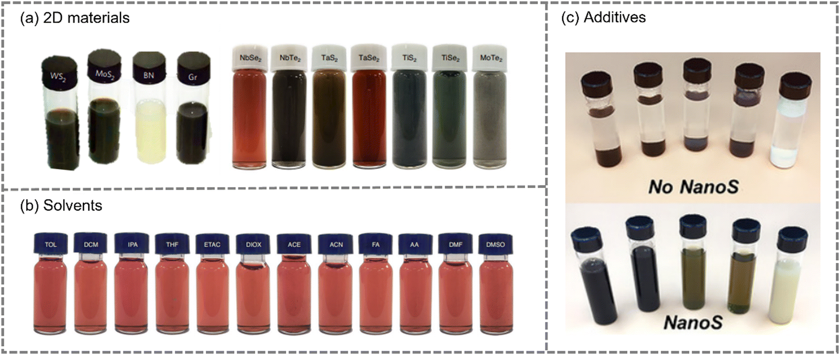 | ||
| Fig. 5 (a) Formulated inks with various 2D vdW materials. Reproduced with permission. (Left98 Copyright 2017, Right44 Copyright 2021, respectively), Publisher Springer Nature. (b) 2D vdW inks with various solvents. Reproduced with permission.44 Copyright 2021, Publisher Springer Nature. (c) Example of additives that prevent reaggregation. Reproduced with permission.99 Copyright 2020, Publisher Wiley-VCH. | ||
Again, 2D vdW materials are naturally favoured for inkjet printing by creating layered 2D contacts. As a host of vdW materials, including ternary and even quaternary families, have been newly discovered and synthesized, many researchers have put in a great deal of effort to fully exploit the aforementioned advantages and produce stable and printable inks for emerging large-area applications. For further developments, continuing efforts in formulating rheologically well-designed air-stable 2D vdW inks are encouraged.
Emerging inkjet-printed 2D vdW device electronic applications
Beyond the single device perspective, the realization of large-area applications based on 2D vdW materials has attracted much attention. At this point, inkjet printing is believed to be a cornerstone of achieving this goal since the attractive advantages of both 2D vdW materials and inkjet printing can create synergetic effects. Based on these reasons, many researchers have combined inkjet printing methodologies and 2D vdW materials. From various passive components, such as conducting electrodes and even a superconducting channel, to active devices, such as all-printed transistors, sensors, and sophisticated circuits, many emerging applications have been proposed, expanding the boundaries in terms of both materials and inkjet printing techniques. Therefore, in this section, we will summarize and discuss recent progress.Inkjet-printed 2D Gr-based electronic devices
In the early stage of the field of printed devices with 2D vdW materials, the demonstration of a single device component such as an electrode, an active channel, and a dielectric layer was usually attempted. As various 2D vdW inks can be formulated, many researchers have been interested in how to realize fully printed active devices or circuit applications with 2D vdW materials. As a result, all-printed devices have been recently reported to be fabricated with representative 2D vdW materials such as Gr and h-BN. For example, Carey et al. successfully fabricated fully printed 2D material-based field-effect transistors (FETs) and circuits on textiles for wearable electronics.33 They used an ink formulation method based on solvent exchange. Firstly, the bulk 2D crystals were effectively exfoliated in a high-boiling point solvent because these solvents can suspend 2D materials without additional stabilisation agents. Subsequently, the exfoliated 2D materials were transferred to a low boiling-point solvent to utilize their rapid evaporation at room temperature. The fully printed Gr/h-BN heterostructure device, where Gr is the active channel, h-BN is the dielectric layer and poly(3,4-ethylenedioxythiophene) polystyrene sulfonate (PEDOT:PSS) is the electrodes, is shown in Fig. 6a. They achieved average field-effect mobility values of 150 ± 15 cm2 V−1 s−1 on polyethylene terephthalate (PET) and 91 ± 29 cm2 V−1 s−1 on polyester textile. In addition, they could demonstrate fully printed complementary inverter, logic gate, and memory behaviours. However, because the active channel was printed Gr, which is not a semiconducting material, the on/off ratio of printed transistors reached only 1.23 ± 0.3, and the gain value of the printed inverter was only approximately 0.1. Therefore, even though they demonstrated the possibility of fully printed, flexible, and stretchable devices and logic circuits on textiles, further improvements are needed for utilization in practical applications.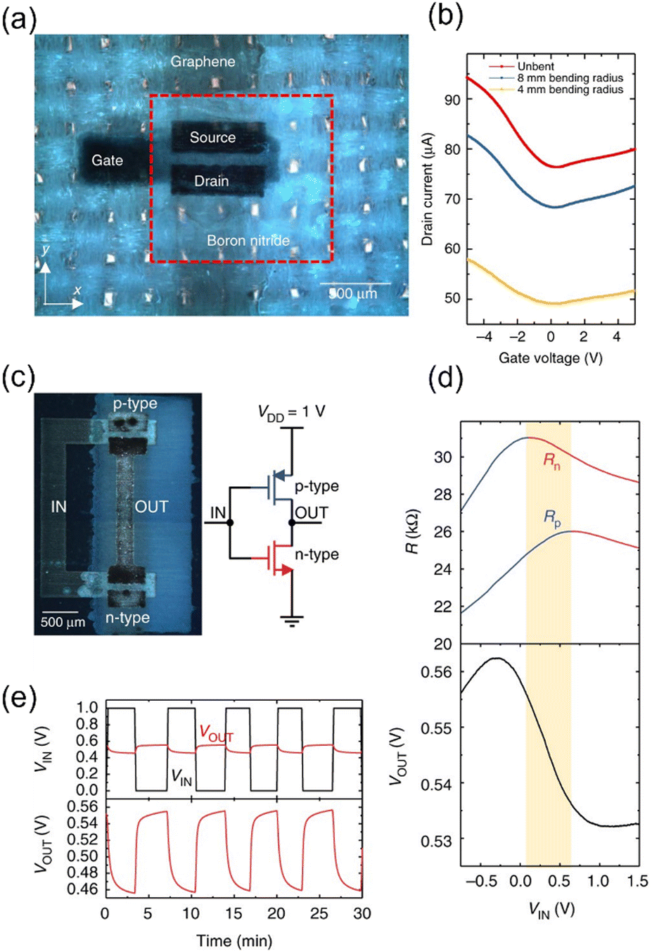 | ||
| Fig. 6 (a) Optical image of a printed FET. (b) Transfer characteristics of the FET for different bending radii. (c) Optical image of an inkjet-printed integrated circuit. (d) Measured resistance and measured static voltage transfer characteristics. (e) Digital VIN and VOUT waveforms measured on an inverter. Reproduced under the terms of the Creative Commons CC BY license.32 | ||
Even if gapless Gr is used as the active layer, combining functional additives can open a new way to demonstrate high-performance devices. Recently, Zeng et al. reported that they could formulate stable aqueous inks by adding Gr quantum dot nanosurfactants.99 The Gr quantum dot (GQD)-added inks could be successfully stabilized in an aqueous system by the reduced surface interfacial tension, showing better printability. Nanoparticle-based surfactants have attracted much attention owing to the synergetic properties of nanoparticles and surfactants. The polyaromatic core structure of the GQD enabled the enhancement of the long-term colloidal stability of graphene ink by introducing the non-covalent π–π interactions between Gr and the GQD. Additionally, the GQD was found to be able to effectively reduce the interfacial tension and alleviate the aggregation of nanomaterials in water. With these GQDs, they could formulate stable MoS2, WS2, Gr, and h-BN inks (Fig. 5c) and fabricate all-printed optoelectronic devices. Not only were post-thermal treatments, which are required when organic surfactants are involved, found to be not required, but also, additional functionality could be introduced due to the bandgap in GQDs attached to the surface of Gr layers. Taking advantage of nanosurfactants, they fabricated bandgap-engineered high-performance printed photodetectors with different device structures having the printed GQDs as a different component, i.e., (i) as an active channel in the Ag/GQD-Gr/Ag structure, (ii) as electrodes in the GQD-Gr/GaN/GQD-Gr structure, and (iii) in cross-plane Ag/GQD-Gr/Al (Fig. 7a–c), and all three devices showed a superior photodetection performance compared to previously reported results, as shown in Fig. 7d–f. Furthermore, they demonstrated an array of UV photodetector devices on a hemispherical glass substrate with a radius of 15 mm as a proof-of-concept.
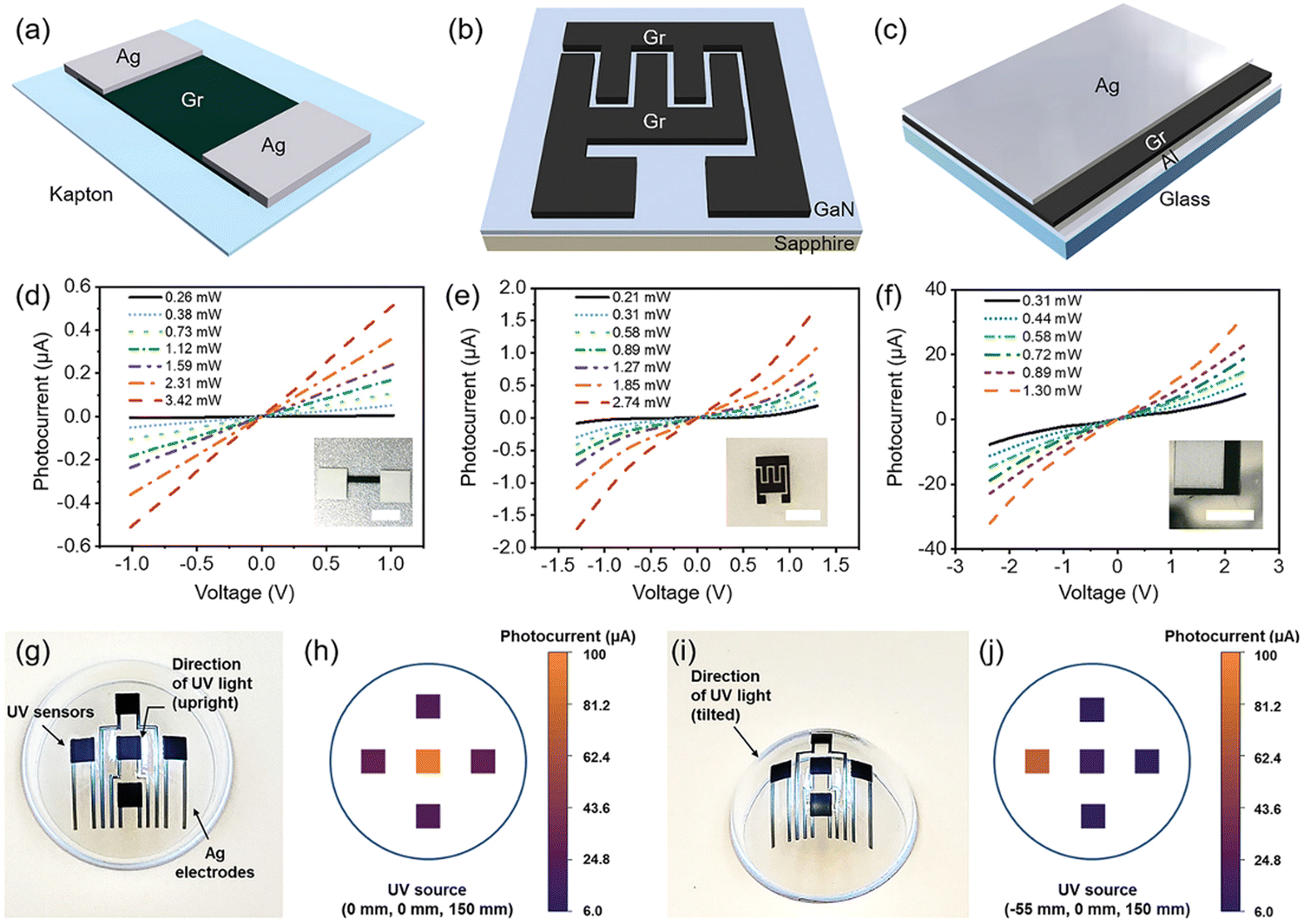 | ||
| Fig. 7 Printed UV sensors using a nanosurfactant ink. (a) Schematic illustrations of an in-plane device with a Gr active channel and (b) a GaN active channel and of (c) a cross-plane device. (d–f) I–V curves corresponding to the three UV detectors shown in (a–c), respectively, under UV illumination. (g) and (i) Optical image of an all-printed 3D photodetector array, and photocurrent mapping results under (h) vertical illumination and (j) tilted-angle illumination. Reproduced with permission.99 Copyright 2020, Publisher Wiley-VCH. | ||
2D TMD-based electronic devices with inkjet-printed components
As the development of exfoliation techniques has enabled the preparation of various 2D vdW inks beyond Gr-based inks, inkjet printing of TMDs has begun. Unlike Gr, many members of the TMD family have an intrinsic bandgap energy, providing more options in inkjet-printed semiconducting devices. Among the variety of TMDs, n-type semiconducting MoS2 has attracted considerable attention due to its attractive properties, such as tuneable bandgap, superior electronic properties, and strong spin–orbit coupling, and has been employed as active channels to overcome the intrinsic limitations of using gapless Gr, as shown in Fig. 1e.45 Before fully exploiting these TMD inks, an alternative method for realization of large-area applications was proposed: the combination of large-area synthesized TMDs and inkjet printing.46,100 Inkjet printing-based film deposition can be a strong candidate to form electrical contacts on 2D materials due to the nondestructive nature of inkjet printing. Recently, Zheng et al. reported that inkjet printing can be a strategy for defect-free metal deposition on 2D vdW materials.101 Contact engineering between the metal electrodes and underlying vdW materials has been intensively studied to improve charge injection at the contact to overcome the vdW gap.52,53,102–105 Additionally, Fermi level pinning effects originating from the interfacial states should be addressed in the field of 2D electronics. According to recent results, high-energy deposition using vacuum evaporation systems may create additional defects at the surface of vdW materials due to high-energy particle collisions that can hinder charge carrier injection and cause the Fermi level pinning effect.106 However, inkjet printing deposition does not require a high-energy deposition process, resulting in defect-free metal deposition on 2D materials.101 The authors reported that the metallic contacts deposited using inkjet printing could form a defect-less interface with the underlying h-BN layer. Additionally, as shown in Fig. 8a and b, they fabricated metal-insulator-metal (MIM) capacitors with metal organic CVD (MOCVD)-grown h-BN via metal deposition by both inkjet printing and evaporation and then compared the electrical breakdown voltages. Fig. 8c shows the I–V curves for the MIM structures with inkjet-printed and evaporated electrodes, where green dots indicate the leakage current at 0.1 V and orange dots show the dielectric breakdown voltages. Owing to the less defective interfaces between inkjet-printed metal electrodes and h-BN layers, the leakage current of the MIM structures with evaporated metal electrodes was on average 100 times higher than that of the counterparts with inkjet-printed electrodes, indicating that the average power consumption would also be approximately 100 times higher. Furthermore, the nondestructive nature of inkjet printing metal deposition would be beneficial to improving the charge injection properties of semiconducting 2D vdW materials, which can be a pathway to realizing high-performance 2D vdW material-based electrical applications.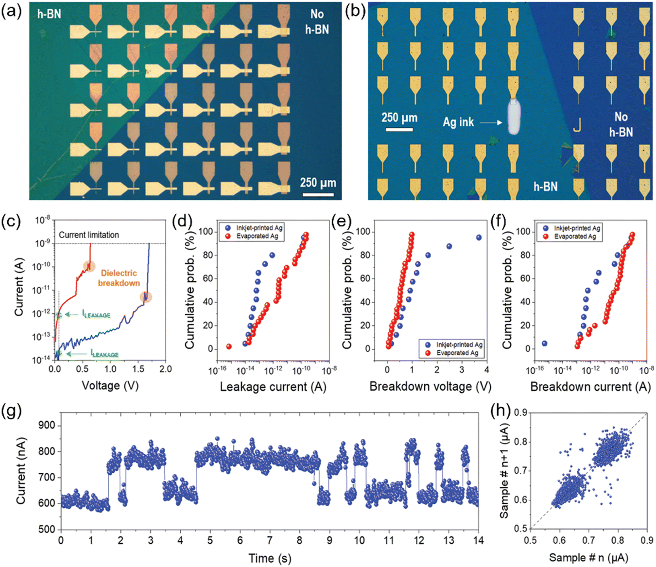 | ||
| Fig. 8 Optical image of an array of Ag/MOCVD h-BN/Ag cross-bar devices with top electrodes deposited with (a) electron beam evaporation and (b) inkjet printing. (c) Representative I–V curves of the devices with top electrodes deposited by electron beam evaporation (red) and inkjet printing (blue). (d–f) Statistical analysis of the leakage current, breakdown voltage, and breakdown current. (g) Stable random telegraph noise (RTN) signal measured in a device with top electrodes deposited by inkjet printing. (h) Weighted scatter plot of the current data evaluated at discrete-time i + 1 vs. (i) Reproduced with permission.101 Copyright 2021, Publisher Wiley-VCH. | ||
As it has been reported that the inkjet printing approach is highly compatible with large-area grown 2D vdW materials, much effort has been dedicated to employing both large-area synthesized 2D vdW films and inkjet printing for emerging applications. This approach would have several advantages over all-2D vdW inkjet printing in terms of electrical performance and the feasibility of fabrication of 2D monolayer devices. Recently, Conti et al. demonstrated high-performance FETs and logic circuits with a CVD-grown MoS2 active channel and inkjet-printed electrodes.107 First, they transferred a CVD-grown MoS2 film onto a paper substrate, which was followed by metal electrode printing. However, for the top gate FETs, another 2D vdW material layer, an h-BN layer, was printed on top of the transferred CVD-grown MoS2. Because the n-type semiconducting monolayer MoS2 intrinsically has a direct bandgap of 1.9 eV, they could obtain highly enhanced logic gating compared to the all-printed Gr FETs and all-printed MoS2 FETs shown in Fig. 1e and 6, respectively. The achieved mobility value was ∼0.8 cm2 V−1 s−1, and the on/off ratio was found to be ∼3 × 10³, which is also much higher than the value of ∼25 for the all-printed MoS2 FET. Furthermore, they also demonstrated logic gates and current mirrors based on inkjet-printed MoS2 FETs on paper substrates. As shown in Fig. 9a and b, they fabricated a resistor-transistor logic inverter with a Gr resistor and Ag electrodes, and its gain value was found to be greater than 25. Considering that the gain of the printed Gr inverter was approximately 0.1, as shown in Fig. 6d, the gain was significantly improved by more than 200 times, even though the printed MoS2 was fabricated on environmentally sustainable and mechanically flexible paper substrates. With the high gain value of the MoS2 FET-based inverter, they could also successfully demonstrate a NAND gate, as shown in Fig. 9d–f. As a further potential application, they additionally demonstrated a current mirror, which is a basic component in analogue electronic circuits.
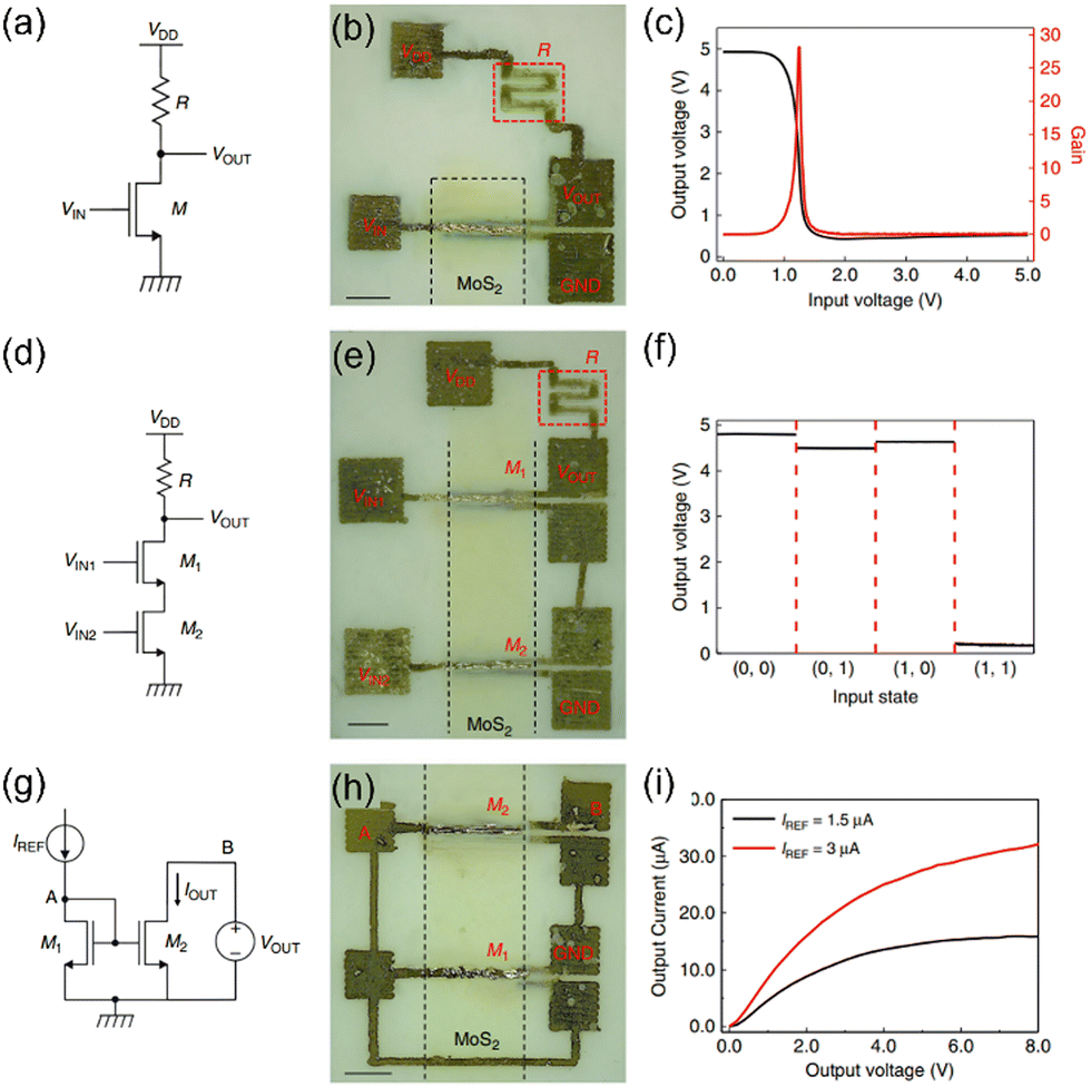 | ||
| Fig. 9 (a) Electrical schematic and (b) optical image of an inverter. (c) Output voltage and voltage gain as a function of the input voltage. (d) Electrical schematic and (e) optical image of a NAND gate. (f) Output voltage of the NAND gate as a function of the input states. (g) Electrical schematic and (h) optical image of a current mirror. (i) Output current of the current mirror as a function of the output voltage for two different references. Reproduced under the terms of the Creative Commons CC BY license.107 | ||
Inkjet-printed vdW superconducting devices
Until recently, demonstrating superconducting devices by using inkjet printing has been very challenging. Continued efforts have recently encouraged a shift of 2D vdW printing research interest from conventional electronics to unprecedented applications by fully exploiting the unique properties of 2D vdW materials. In addition, as diverse novel 2D vdW materials have been synthesized and formulated into printable inks with the help of state-of-the-art electrochemical exfoliation methods, Li et al. could produce large-area high-quality printable 2D NbSe2 monolayers and demonstrate superconducting devices by using inkjet printing. By introducing quaternary ammonium cations as a cathodic intercalant, they could successfully exfoliate and formulate Nb(Se/Te)2, Ta(S/Se)2, Ti(S/Se)2, and MoTe2 inks, as shown on the left side of Fig. 5a.44 Most importantly, the large size of the 2D flakes facilitates a channel with fewer barriers between the layered flakes when they form a connected conducting channel. In contrast, for electrochemical exfoliation under mild external energy conditions, the general LPE process includes high-power ultrasonication to exfoliate flakes and prevent reaggregation. Consequently, the high-power ultrasonication process will inevitably create additional defects, simultaneously producing small size flakes. In this context, optimized conditions are necessary to exfoliate less defective, larger 2D flakes. Although lithium ions have been widely used for electrochemical LPE methods, intercalated lithium ions have been known to distort lattice structures, changing the crystal phase. However, Li et al. could produce high-quality large flakes by alternatively employing tetrabutylammonium cations. The yield of 1–5 layers of the 2D superconducting film was confirmed to be greater than 80%. The lateral dimension of exfoliated NbSe2 monolayers was found to be larger than a few hundred micrometres (Fig. 10a). Additionally, the quality of the exfoliated flakes was good enough to demonstrate superconducting device applications, as shown in the scanning tunnelling microscopy (STM) image of Fig. 10b. In addition to STM analysis, they also measured the electrical properties of a Hall bar device with an as-exfoliated flake to evaluate the quality of exfoliated flakes. Impurity scattering and defects lead to a large residual resistance (i.e., a small residual resistance ratio (RRR)). The RRR value of electrochemically exfoliated NbSe2 flakes was determined to be approximately 3.5, which is smaller than that of mechanically exfoliated NbSe2 but larger than that of CVD-grown flakes, implying less disorder in the electrochemically exfoliated NbSe2 flakes. Additionally, the superconducting transition temperature of printed NbSe2 was found to be ∼3.2 K, as shown in Fig. 10c, which is consistent with the previously reported value. With high-quality 2D vdW inks, the authors could even demonstrate well-operated Josephson junction behaviour. In particular, this novel LPE method not only provides high-quality flakes but also allows the formulation of stable NbSe2 inks for 2D and even 3D printing processes. In addition, the solvent protection and self-cleaning nature of 2D vdW materials prevent potential degradation of device performance without additional encapsulation layers during the time-consuming fabrication process. As a result, the 3D printed structure, shown in Fig. 10e, showed a diamagnetic transition at ∼6.8 K, which is a representative signature of the superconducting transition. The wafer-scale printed NbSe2 pattern also successfully showed superconducting behaviour, as shown in Fig. 10i–l. Interestingly, the printed NbSe2 wire showed both bulk-like superconducting transition behaviour and a monolayer-like upper critical field. The authors assumed that this might be due to the mixed effects from Pauli paramagnetism and spin–orbit scattering in NbSe2 at the interlayer Josephson junctions.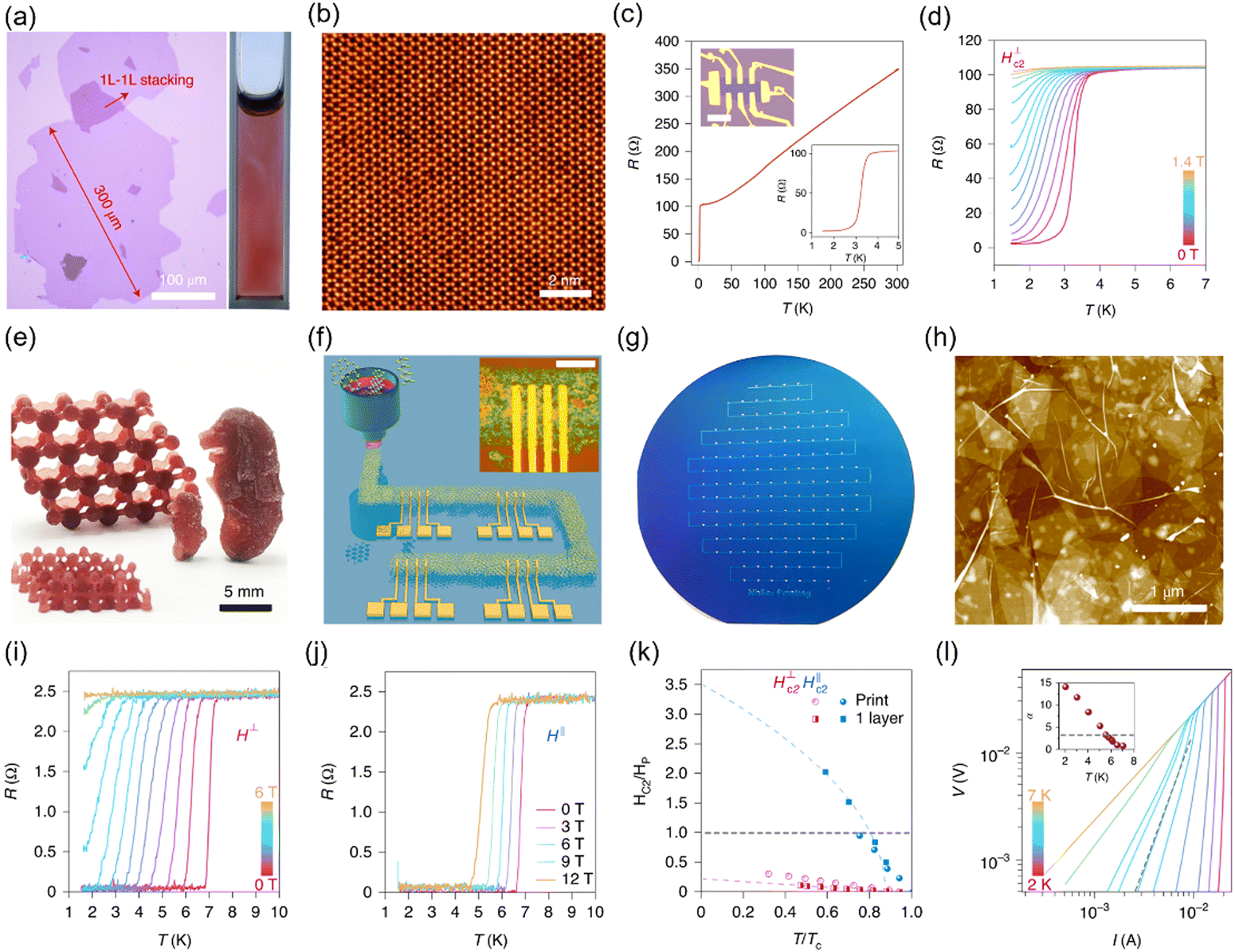 | ||
| Fig. 10 (a) Optical image of NbSe2 monolayer flakes. The right inset shows a photograph of tetrapropylammonium (TPA)-exfoliated NbSe2 flakes in propylene carbonate (PC). (b) Atomically resolved scanning transmission electron microscopy annular dark-field (STEM-ADF) image of an exfoliated NbSe2 flake. (c) Temperature-dependent longitudinal resistance for a monolayer NbSe2 device. (d) Temperature-dependent longitudinal resistance under various perpendicular magnetic fields. (e) Photograph of models fabricated by 3D printing. (f) Schematic illustration, (g) photograph and (h) atomic force microscopy (AFM) image of an inkjet-printed NbSe2 wire on a 4-inch SiO2/Si wafer. (i and j) Temperature-dependent longitudinal resistance of a printed NbSe2 film under (i) out-of-plane and (j) in-plane magnetic fields. (k) Critical field as a function of transition temperature for printed NbSe2 under out-of-plane and in-plane magnetic fields. (l) Voltage–current characteristics at different temperatures. Reproduced with permission.44 Copyright 2021, Publisher Springer Nature. | ||
Challenges and outlook
Despite rapid progress and developments, there are remaining hurdles that should be addressed to fully utilize the inkjet printing strategy for future applications based on 2D vdW materials. First, the printing of a uniform 2D vdW monolayer should be guaranteed because the atomically thin nature of 2D vdW materials is one of the most attractive features. In addition, the absence of dangling bonds on their surfaces reduces the thickness of vdW films down to the atomic scale, which is challenging for conventional 3D semiconductors with a large number of reactive dangling bonds. To successfully employ the advantages of 2D vdW materials, the printed channel should be thinned down to the monolayer limit, although layer-by-layer controlling of the LPE is a remaining issue. Furthermore, a variety of 2D semiconducting vdW materials have a direct bandgap in the monolayer system. Thus, the printing of monolayer 2D vdW materials is also encouraged for optoelectronic applications. From this perspective, many researchers have tried to print a monolayer of 2D materials. As illustrated in Fig. 11a, meeting this demand by adjusting the printing conditions, such as the temperature of the substrate, to control the Marangoni convection and the capillary flow, thus removing excessive liquid, has been attempted.108 However, the liquid removal process is difficult to employ in the inkjet printing process, and the deposited film was found to have uncovered regions that hinder charge transport. Recently, spin-coating of electrochemically exfoliated vdW materials to obtain vdW layered films was found to be more suitable for depositing uniform 2D vdW films for flexible and stretchable applications than CVD growth of films because shear movement in the lateral direction is allowed due to the weak vdW interaction and network-like morphology, while the CVD-grown film cannot be freely stretched due to the strong in-plane covalent bonding between atoms.109 This result indicates that a partially staggered structure of monolayer flakes can also be demonstrated by using inkjet printing to deliver stretchability while maintaining the unique properties of monolayer vdW materials. Although the bottom-up synthesis methods are known to produce lower quality 2D materials for the large-area applications so far, these methods can be alternatively used for the monolayer deposition if the remaining quality issue could be addressed, since they have attractive potentials, such as high controllability of surface morphology, crystallite size, and dopant.110 In addition, the combination of inkjet printing and CVD synthesis can also be a feasible solution to deposit 2D vdW monolayers. Wan et al. directly printed the precursor onto the target substrate on demand, which was followed by CVD synthesis to generate a large-area inkjet-printed patterned monolayer MoS2 film.111 Although this approach can provide a directly patterned monolayer of MoS2, it can only be conducted on limited substrates compatible with a high-temperature process (>750 °C) for CVD synthesis. In addition, multiple passes of printing and an interspersed CVD process would be essential to realize heterostructures, so the sequentially printed precursors and the subsequent CVD process can affect the underlying layers. Thus, a reliable monolayer printing method should be proposed to fully exploit the advantages of 2D vdW materials.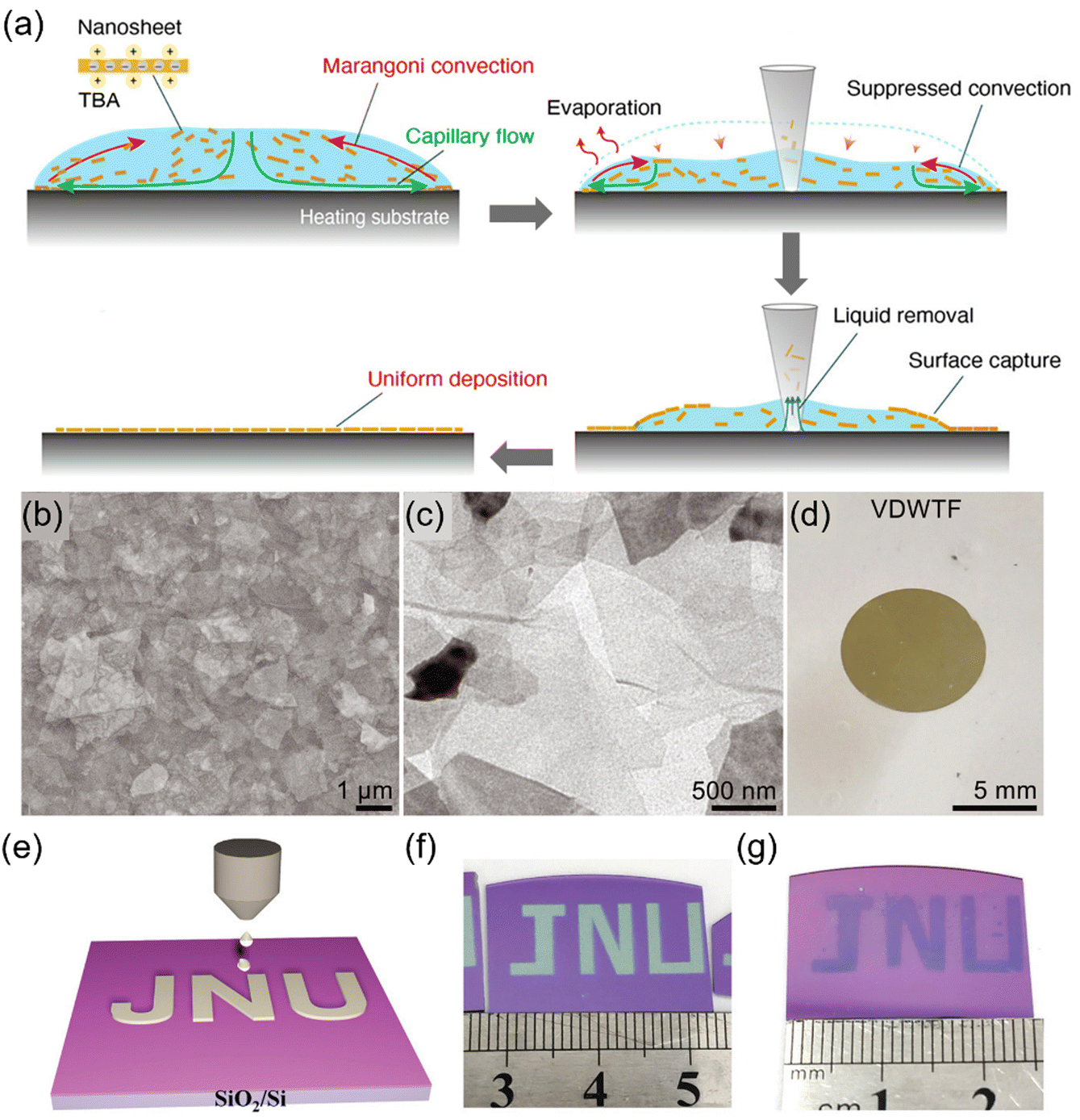 | ||
| Fig. 11 (a) Plausible model for 2D nanosheet tiling. Reproduced with permission.108 Copyright 2020, Publisher ACS. (b) Scanning electron microscopy (SEM) and (c) transmission electron microscopy (TEM) images showing a vdW thin film assembled from staggered 2D nanosheets. (d) Photograph of the vdW thin film floating on water. Reproduced with permission.109 Copyright 2022, Publisher AAAS. (e) Schematic of printed precursors on a substrate. (f) Photograph of the printed precursor. (g) Photograph of the patterned MoS2 film after CVD growth. Reproduced with permission.111 Copyright 2021, Publisher Wiley-VCH. | ||
Second, the realization of 2D vdW heterostructures should be obtainable. The ultimate goal of vdW inkjet printing is to continuously manufacture 2D vdW material-based devices with a high degree of design freedom on target substrates. Beyond depositing only single 2D vdW layers, large-area electronic devices, e.g., transistors, memory devices, sensors, and even logics, should be integrated on a substrate in monolithic manufacturing. Therefore, the printing of stacked heterostructures with various types of 2D vdW inks needs to be pursued, considering their rheological and interfacial properties. It should be noted that the interfacial properties between the printed vdW flakes should be also carefully optimized where they can hugely affect device performance due to their 2D nature. Particularly, the interfaces formed between inter-flakes by inkjet printing can be different from the pristine counterpart existing in the bulk crystals owing to their weak vdW bonding nature along the z-axis. In this sense, it is natural to assume that the interfacial properties between inkjet-printed vdW materials could be inferior compared to those of bulk crystals.
Third, environmentally stable printable vdW materials should be investigated. Until now, emerging novel vdW materials have been synthesized, however, their relatively poor air stability can be a critical bottleneck exhibiting rapid degradation of their unique characteristics under ambient conditions. For example, we strongly believe that the applications based on magnetic vdW materials would be realized by using the inkjet printing technique as well in the near future since there have been many efforts to explore vdW magnetic materials, including CrI3 and Fe3GeTe2, which have received attention as emerging magnetic vdW materials. Because it would be extremely challenging where such magnetic and topological materials are typically unstable under ambient conditions, so they must only be used in a controlled environment.112,113 Due to these difficulties, there are barely any demonstrations to date on inkjet printing of 2D vdW materials for magnetism, twistronics, and other related topics. In addition, the electrical or optoelectronic properties of vdW materials can also be degraded by exposure to solvents During the continuous inkjet printing process to fabricate vertically stacked heterostructures, the vdW materials will inevitably be exposed to the sequentially dropped ink solvents. Furthermore, as the thickness of vdW materials decreases, i.e., the surface-to-volume ratio increases, the printed vdW materials will be largely affected by the surrounding environment. Thus, introducing suitable additives or binders may be beneficial for stabilizing the printable environment-sensitive vdW materials. Additionally, orthogonal solvents that cannot affect the underlying layers should be used to disperse 2D vdW materials while considering the printability.
In conclusion, 2D vdW materials have shown promising opportunities to demonstrate a new class of electronics compared to other low-dimensional materials. Recently, as practical 2D vdW device applications have been pursued, many research groups have been dedicating much effort, such as employing advanced manufacturing to demonstrate large-area, reliable, and high-performance 2D vdW heterostructures. Owing to the solution processability of 2D vdW materials, inkjet printing has been rising as a suitable approach for realizing emerging 2D vdW applications. Inkjet printing can pave a promising pathway to produce low-cost and scalable heterostructures with the DOD processability. Although there are remaining challenges, we believe that the attractive advantages of inkjet printing will ensure great synergetic effects with 2D vdW materials, exploiting their unique characteristics, and further improving the quality of life to a higher level.
Conflicts of interest
There are no conflicts to declare.Acknowledgements
The authors appreciate the financial support from the National Research Foundation of Korea (NRF) grant funded by the Korean government (the Ministry of Science and ICT) (No. NRF-2020R1A2C4001948, NRF-2021R1C1C2091728 and NRF-2021R1A2C3004783), and the Korea Institute of Science and Technology (KIST) Future Resource Research Program (2E31811).Notes and references
- S. Han, M. K. Kim, B. Wang, D. S. Wie, S. Wang and C. H. Lee, Adv. Mater., 2016, 28, 10257–10265 CrossRef CAS PubMed.
- D.-M. Drotlef, M. Amjadi, M. Yunusa and M. Sitti, Adv. Mater., 2017, 29, 1701353 CrossRef PubMed.
- A. Koh, D. Kang, Y. Xue, S. Lee, R. M. Pielak, J. Kim, T. Hwang, S. Min, A. Banks, P. Bastien, M. C. Manco, L. Wang, K. R. Ammann, K.-I. Jang, P. Won, S. Han, R. Ghaffari, U. Paik, M. J. Slepian, G. Balooch, Y. Huang and J. A. Rogers, Sci. Transl. Med., 2016, 8, 366ra165 Search PubMed.
- S. Imani, A. J. Bandodkar, A. M. V. Mohan, R. Kumar, S. Yu, J. Wang and P. P. Mercier, Nat. Commun., 2016, 7, 11650 CrossRef CAS PubMed.
- W. Gao, S. Emaminejad, H. Y. Y. Nyein, S. Challa, K. Chen, A. Peck, H. M. Fahad, H. Ota, H. Shiraki, D. Kiriya, D.-H. Lien, G. A. Brooks, R. W. Davis and A. Javey, Nature, 2016, 529, 509–514 CrossRef CAS PubMed.
- L. Pi, L. Li, K. Liu, Q. Zhang, H. Li and T. Zhai, Adv. Funct. Mater., 2019, 29, 1904932 CrossRef CAS.
- M. Och, M.-B. Martin, B. Dlubak, P. Seneor and C. Mattevi, Nanoscale, 2021, 13, 2157–2180 RSC.
- K. Cho, J. Pak, S. Chung and T. Lee, ACS Nano, 2019, 13, 9713–9734 CrossRef CAS PubMed.
- K. S. Burch, D. Mandrus and J.-K. Park, Nature, 2018, 563, 47–52 CrossRef CAS PubMed.
- A. H. Castro Neto, F. Guinea, N. M. R. Peres, K. S. Novoselov and A. K. Geim, Rev. Mod. Phys., 2009, 81, 109–162 CrossRef CAS.
- K. S. Novoselov, A. Mishchenko, A. Carvalho and A. H. Castro Neto, Science, 2016, 353, aac9439 CrossRef CAS PubMed.
- M. Gibertini, M. Koperski, A. F. Morpurgo and K. S. Novoselov, Nat. Nanotechnol., 2019, 14, 408–419 CrossRef CAS PubMed.
- D. Jariwala, V. K. Sangwan, L. J. Lauhon, T. J. Marks and M. C. Hersam, ACS Nano, 2014, 8, 1102–1120 CrossRef CAS PubMed.
- G. Fiori, F. Bonaccorso, G. Iannaccone, T. Palacios, D. Neumaier, A. Seabaugh, S. K. Banerjee and L. Colombo, Nat. Nanotechnol., 2014, 9, 768–779 CrossRef CAS PubMed.
- S. J. Kim, K. Choi, B. Lee, Y. Kim and B. H. Hong, Annu. Rev. Mater. Res., 2015, 45, 63–84 CrossRef CAS.
- Q. H. Wang, K. Kalantar-Zadeh, A. Kis, J. N. Coleman and M. S. Strano, Nat. Nanotechnol., 2012, 7, 699–712 CrossRef CAS PubMed.
- C.-C. Chiang, V. Ostwal, P. Wu, C.-S. Pang, F. Zhang, Z. Chen and J. Appenzeller, Appl. Phys. Rev., 2021, 8, 021306 CAS.
- J. Li, M. C. Lemme and M. Östling, Chem. Phys. Chem., 2014, 15, 3427–3434 CrossRef CAS PubMed.
- R. Worsley, L. Pimpolari, D. McManus, N. Ge, R. Ionescu, J. A. Wittkopf, A. Alieva, G. Basso, M. Macucci, G. Iannaccone, K. S. Novoselov, H. Holder, G. Fiori and C. Casiraghi, ACS Nano, 2019, 13, 54–60 CrossRef CAS PubMed.
- K. Hassan, M. J. Nine, T. T. Tung, N. Stanley, P. L. Yap, H. Rastin, L. Yu and D. Losic, Nanoscale, 2020, 12, 19007–19042 RSC.
- G. Hu, J. Kang, L. W. T. Ng, X. Zhu, R. C. T. Howe, C. G. Jones, M. C. Hersam and T. Hasan, Chem. Soc. Rev., 2018, 47, 3265–3300 RSC.
- A. Capasso, A. E. Del Rio Castillo, H. Sun, A. Ansaldo, V. Pellegrini and F. Bonaccorso, Solid State Commun., 2015, 224, 53–63 CrossRef CAS.
- L. W. T. Ng, G. Hu, R. C. T. Howe, X. Zhu, Z. Yang, C. G. Jones and T. Hasan, Printing of Graphene and Related 2D Materials: Technology, Formulation and Applications, Springer International Publishing, Cham, 2019 Search PubMed.
- J. Liang, C. Jiang and W. Wu, Appl. Phys. Rev., 2021, 8, 021319 CAS.
- R. Yang, J. Zhou, C. Yang, L. Qiu and H. Cheng, Adv. Mater. Technol., 2020, 5, 1901066 CrossRef CAS.
- S. Chung, K. Cho and T. Lee, Adv. Sci., 2019, 6, 1801445 CrossRef PubMed.
- Z. Lin, Y. Huang and X. Duan, Nat. Electron., 2019, 2, 378–388 CrossRef.
- E. Cannavò, D. Marian, E. G. Marín, G. Iannaccone and G. Fiori, Phys. Rev. B, 2021, 104, 085433 CrossRef.
- F. Wang, J. H. Gosling, G. F. Trindade, G. A. Rance, O. Makarovsky, N. D. Cottam, Z. Kudrynskyi, A. G. Balanov, M. T. Greenaway, R. D. Wildman, R. Hague, C. Tuck, T. M. Fromhold and L. Turyanska, Adv. Funct. Mater., 2021, 31, 2007478 CrossRef CAS.
- S. Lu and A. D. Franklin, Nanoscale, 2020, 12, 23371–23390 RSC.
- J. Zhou, J. Lin, X. Huang, Y. Zhou, Y. Chen, J. Xia, H. Wang, Y. Xie, H. Yu, J. Lei, D. Wu, F. Liu, Q. Fu, Q. Zeng, C.-H. Hsu, C. Yang, L. Lu, T. Yu, Z. Shen, H. Lin, B. I. Yakobson, Q. Liu, K. Suenaga, G. Liu and Z. Liu, Nature, 2018, 556, 355–359 CrossRef CAS PubMed.
- J.-W. T. Seo, J. Zhu, V. K. Sangwan, E. B. Secor, S. G. Wallace and M. C. Hersam, ACS Appl. Mater. Interfaces, 2019, 11, 5675–5681 CrossRef CAS PubMed.
- T. Carey, S. Cacovich, G. Divitini, J. Ren, A. Mansouri, J. M. Kim, C. Wang, C. Ducati, R. Sordan and F. Torrisi, Nat. Commun., 2017, 8, 1202 CrossRef PubMed.
- R. F. Hossain, M. Min and A. B. Kaul, MRS Adv., 2019, 4, 621–627 CrossRef CAS.
- D. J. Finn, M. Lotya, G. Cunningham, R. J. Smith, D. McCloskey, J. F. Donegan and J. N. Coleman, J. Mater. Chem. C, 2014, 2, 925–932 RSC.
- C. Casiraghi, M. Macucci, K. Parvez, R. Worsley, Y. Shin, F. Bronte, C. Borri, M. Paggi and G. Fiori, Carbon, 2018, 129, 462–467 CrossRef CAS.
- T. Juntunen, H. Jussila, M. Ruoho, S. Liu, G. Hu, T. Albrow-Owen, L. W. T. Ng, R. C. T. Howe, T. Hasan, Z. Sun and I. Tittonen, Adv. Funct. Mater., 2018, 28, 1800480 CrossRef.
- J. Li, F. Rossignol and J. Macdonald, Lab Chip, 2015, 15, 2538–2558 RSC.
- E. B. Secor, P. L. Prabhumirashi, K. Puntambekar, M. L. Geier and M. C. Hersam, J. Phys. Chem. Lett., 2013, 4, 1347–1351 CrossRef CAS PubMed.
- J. Li, M. M. Naiini, S. Vaziri, M. C. Lemme and M. Östling, Adv. Funct. Mater., 2014, 24, 6524–6531 CrossRef CAS.
- P. He and B. Derby, 2D Mater., 2017, 4, 021021 CrossRef.
- F. Torrisi, T. Hasan, W. Wu, Z. Sun, A. Lombardo, T. S. Kulmala, G.-W. Hsieh, S. Jung, F. Bonaccorso, P. J. Paul, D. Chu and A. C. Ferrari, ACS Nano, 2012, 6, 2992–3006 CrossRef CAS PubMed.
- X. Jiang, W. Li, T. Hai, R. Yue, Z. Chen, C. Lao, Y. Ge, G. Xie, Q. Wen and H. Zhang, npj 2D Mater. Appl., 2019, 3, 34 CrossRef.
- J. Li, P. Song, J. Zhao, K. Vaklinova, X. Zhao, Z. Li, Z. Qiu, Z. Wang, L. Lin, M. Zhao, T. S. Herng, Y. Zuo, W. Jonhson, W. Yu, X. Hai, P. Lyu, H. Xu, H. Yang, C. Chen, S. J. Pennycook, J. Ding, J. Teng, A. H. Castro Neto, K. S. Novoselov and J. Lu, Nat. Mater., 2021, 20, 181–187 CrossRef CAS PubMed.
- A. G. Kelly, T. Hallam, C. Backes, A. Harvey, A. S. Esmaeily, I. Godwin, J. Coelho, V. Nicolosi, J. Lauth, A. Kulkarni, S. Kinge, L. D. A. Siebbeles, G. S. Duesberg and J. N. Coleman, Science, 2017, 356, 69–73 CrossRef CAS PubMed.
- T.-Y. Kim, J. Ha, K. Cho, J. Pak, J. Seo, J. Park, J.-K. Kim, S. Chung, Y. Hong and T. Lee, ACS Nano, 2017, 11, 10273–10280 CrossRef CAS PubMed.
- Y. Zhang, T.-R. Chang, B. Zhou, Y.-T. Cui, H. Yan, Z. Liu, F. Schmitt, J. Lee, R. Moore, Y. Chen, H. Lin, H.-T. Jeng, S.-K. Mo, Z. Hussain, A. Bansil and Z.-X. Shen, Nat. Nanotechnol., 2014, 9, 111–115 CrossRef CAS PubMed.
- J. Su, M. Wang, G. Liu, H. Li, J. Han and T. Zhai, Adv. Sci., 2020, 7, 2001722 CrossRef CAS PubMed.
- D. Dumcenco and E. Giannini, J. Cryst. Growth, 2020, 548, 125799 CrossRef CAS.
- M. Tanaka, Y. Fujishiro, M. Mogi, Y. Kaneko, T. Yokosawa, N. Kanazawa, S. Minami, T. Koretsune, R. Arita, S. Tarucha, M. Yamamoto and Y. Tokura, Nano Lett., 2020, 20, 7476–7481 CrossRef CAS PubMed.
- D. Hu, G. Xu, L. Xing, X. Yan, J. Wang, J. Zheng, Z. Lu, P. Wang, X. Pan and L. Jiao, Angew. Chem., 2017, 129, 3665–3669 CrossRef.
- L. Wang, I. Meric, P. Y. Huang, Q. Gao, Y. Gao, H. Tran, T. Taniguchi, K. Watanabe, L. M. Campos, D. A. Muller, J. Guo, P. Kim, J. Hone, K. L. Shepard and C. R. Dean, Science, 2013, 342, 614–617 CrossRef CAS PubMed.
- X. Cui, G.-H. Lee, Y. D. Kim, G. Arefe, P. Y. Huang, C.-H. Lee, D. A. Chenet, X. Zhang, L. Wang, F. Ye, F. Pizzocchero, B. S. Jessen, K. Watanabe, T. Taniguchi, D. A. Muller, T. Low, P. Kim and J. Hone, Nat. Nanotechnol., 2015, 10, 534–540 CrossRef CAS PubMed.
- B. Radisavljevic, A. Radenovic, J. Brivio, V. Giacometti and A. Kis, Nat. Nanotechnol., 2011, 6, 147–150 CrossRef CAS PubMed.
- J.-K. Kim, K. Cho, J. Jang, K.-Y. Baek, J. Kim, J. Seo, M. Song, J. Shin, J. Kim, S. S. Parkin, J.-H. Lee, K. Kang and T. Lee, Adv. Mater., 2021, 33, 2101598 CrossRef CAS PubMed.
- B. Huang, G. Clark, D. R. Klein, D. MacNeill, E. Navarro-Moratalla, K. L. Seyler, N. Wilson, M. A. McGuire, D. H. Cobden, D. Xiao, W. Yao, P. Jarillo-Herrero and X. Xu, Nat. Nanotechnol., 2018, 13, 544–548 CrossRef CAS PubMed.
- L. Webster and J.-A. Yan, Phys. Rev. B, 2018, 98, 144411 CrossRef CAS.
- Y. Deng, Y. Yu, Y. Song, J. Zhang, N. Z. Wang, Z. Sun, Y. Yi, Y. Z. Wu, S. Wu, J. Zhu, J. Wang, X. H. Chen and Y. Zhang, Nature, 2018, 563, 94–99 CrossRef CAS PubMed.
- M. M. Ugeda, A. J. Bradley, Y. Zhang, S. Onishi, Y. Chen, W. Ruan, C. Ojeda-Aristizabal, H. Ryu, M. T. Edmonds, H.-Z. Tsai, A. Riss, S.-K. Mo, D. Lee, A. Zettl, Z. Hussain, Z.-X. Shen and M. F. Crommie, Nat. Phys., 2016, 12, 92–97 Search PubMed.
- X. Xi, L. Zhao, Z. Wang, H. Berger, L. Forró, J. Shan and K. F. Mak, Nat. Nanotechnol., 2015, 10, 765–769 CrossRef CAS PubMed.
- K.-R. Jeon, K. Cho, A. Chakraborty, J.-C. Jeon, J. Yoon, H. Han, J.-K. Kim and S. S. Parkin, ACS Nano, 2021, 15, 16819–16827 CrossRef CAS PubMed.
- P. Zareapour, A. Hayat, S. Y. F. Zhao, M. Kreshchuk, A. Jain, D. C. Kwok, N. Lee, S.-W. Cheong, Z. Xu, A. Yang, G. D. Gu, S. Jia, R. J. Cava and K. S. Burch, Nat. Commun., 2012, 3, 1056 CrossRef PubMed.
- W. Liao, S. Zhao, F. Li, C. Wang, Y. Ge, H. Wang, S. Wang and H. Zhang, Nanoscale Horiz., 2020, 5, 787–807 RSC.
- Y. Liu, N. O. Weiss, X. Duan, H.-C. Cheng, Y. Huang and X. Duan, Nat. Rev. Mater., 2016, 1, 1–17 RSC.
- A. Chaves, J. G. Azadani, H. Alsalman, D. R. da Costa, R. Frisenda, A. J. Chaves, S. H. Song, Y. D. Kim, D. He, J. Zhou, A. Castellanos-Gomez, F. M. Peeters, Z. Liu, C. L. Hinkle, S.-H. Oh, P. D. Ye, S. J. Koester, Y. H. Lee, P. Avouris, X. Wang and T. Low, npj 2D Mater. Appl., 2020, 4, 29 CrossRef CAS.
- K. Yasuda, X. Wang, K. Watanabe, T. Taniguchi and P. Jarillo-Herrero, Science, 2021, 372, 1458–1462 CrossRef CAS PubMed.
- A. Weston, E. G. Castanon, V. Enaldiev, F. Ferreira, S. Bhattacharjee, S. Xu, H. Corte-León, Z. Wu, N. Clark, A. Summerfield, T. Hashimoto, Y. Gao, W. Wang, M. Hamer, H. Read, L. Fumagalli, A. V. Kretinin, S. J. Haigh, O. Kazakova, A. K. Geim, V. I. Fal’ko and R. Gorbachev, Nat. Nanotechnol., 2022, 1–6 Search PubMed.
- Y. Cao, V. Fatemi, S. Fang, K. Watanabe, T. Taniguchi, E. Kaxiras and P. Jarillo-Herrero, Nature, 2018, 556, 43–50 CrossRef CAS PubMed.
- R. Frisenda, E. Navarro-Moratalla, P. Gant, D. P. D. Lara, P. Jarillo-Herrero, R. V. Gorbachev and A. Castellanos-Gomez, Chem. Soc. Rev., 2018, 47, 53–68 RSC.
- J. F. Sierra, J. Fabian, R. K. Kawakami, S. Roche and S. O. Valenzuela, Nat. Nanotechnol., 2021, 16, 856–868 CrossRef CAS PubMed.
- W. Han, APL Mater., 2016, 4, 032401 CrossRef.
- X. Lin, W. Yang, K. L. Wang and W. Zhao, Nat. Electron., 2019, 2, 274–283 CrossRef CAS.
- Y. Zhou and L.-D. Zhao, Adv. Mater., 2017, 29, 1702676 CrossRef PubMed.
- K. Kanahashi, J. Pu and T. Takenobu, Adv. Energy Mater., 2020, 10, 1902842 CrossRef CAS.
- C. Bao, P. Tang, D. Sun and S. Zhou, Nat. Rev. Phys., 2022, 4, 33–48 CrossRef.
- Y. Deng, Y. Yu, M. Z. Shi, Z. Guo, Z. Xu, J. Wang, X. H. Chen and Y. Zhang, Science, 2020, 367, 895–900 CrossRef CAS PubMed.
- A. A. Soluyanov, D. Gresch, Z. Wang, Q. Wu, M. Troyer, X. Dai and B. A. Bernevig, Nature, 2015, 527, 495–498 CrossRef CAS PubMed.
- M. Blei, J. L. Lado, Q. Song, D. Dey, O. Erten, V. Pardo, R. Comin, S. Tongay and A. S. Botana, Appl. Phys. Rev., 2021, 8, 021301 CAS.
- L. Zhang, J. Zhou, H. Li, L. Shen and Y. P. Feng, Appl. Phys. Rev., 2021, 8, 021308 CAS.
- J. Yao and G. Yang, Adv. Sci., 2022, 9, 2103036 CrossRef PubMed.
- A. Ciesielskia and P. Samorì, Chem. Soc. Rev., 2014, 43, 381–398 RSC.
- Y. Hernandez, V. Nicolosi, M. Lotya, F. M. Blighe, Z. Sun, S. De, I. T. McGovern, B. Holland, M. Byrne, Y. K. Gun’Ko, J. J. Boland, P. Niraj, G. Duesberg, S. Krishnamurthy, R. Goodhue, J. Hutchison, V. Scardaci, A. C. Ferrari and J. N. Coleman, Nat. Nanotechnol., 2008, 3, 563–568 CrossRef CAS PubMed.
- Y. Yang, X. Ji, X. Yang, C. Wang, W. Song, Q. Chen and C. E. Banks, RSC Adv., 2013, 3, 16130 RSC.
- L. Li, D. Zhang, Y. Gao, J. Deng, Y. Gou and J. Fang, J. Alloys Compd., 2021, 862, 158551 CrossRef CAS.
- A. Ambrosi and M. Pumera, Chem. Soc. Rev., 2018, 47, 7213–7224 RSC.
- S. Yang, S. Brüller, Z.-S. Wu, Z. Liu, K. Parvez, R. Dong, F. Richard, P. Samorì, X. Feng and K. Müllen, J. Am. Chem. Soc., 2015, 137, 13927–13932 CrossRef CAS PubMed.
- T. C. Achee, W. Sun, J. T. Hope, S. G. Quitzau, C. B. Sweeney, S. A. Shah, T. Habib and M. J. Green, Sci. Rep., 2018, 8, 14525 CrossRef PubMed.
- H. Lee, M. Koo, C. Park, M. Patel, H. Han, T. H. Park, P. Kumar, W.-G. Koh and C. Park, Nano Res., 2020, 13, 2726–2734 CrossRef CAS.
- L. Li, D. Zhang, Y. Gao, J. Deng, Y. Gou and J. Fang, J. Alloys Compd., 2021, 862, 158551 CrossRef CAS.
- B.-J. de Gans, P. C. Duineveld and U. S. Schubert, Adv. Mater., 2004, 16, 203–213 CrossRef CAS.
- N. C. Raut and K. Al-Shamery, J. Mater. Chem. C, 2018, 6, 1618–1641 RSC.
- B. Derby, Annu. Rev. Mater. Res., 2010, 40, 395–414 CrossRef CAS.
- K. Kouroupis-Agalou, A. Liscio, E. Treossi, L. Ortolani, V. Morandi, N. Maria Pugno and V. Palermo, Nanoscale, 2014, 6, 5926–5933 RSC.
- X. Liu, T.-J. Tarn, F. Huang and J. Fan, Particuology, 2015, 19, 1–13 CrossRef CAS.
- J. E. Fromm, IBM J. Res. Dev., 1984, 28, 322–333 Search PubMed.
- S. Mueller, E. W. Llewellin and H. M. Mader, Proc. R. Soc. A, 2010, 466, 1201–1228 CrossRef CAS.
- N. Reis and B. Derby, Mater. Res. Soc. Symp. Proc., 2000, 624, 65–70 CrossRef.
- D. McManus, S. Vranic, F. Withers, V. Sanchez-Romaguera, M. Macucci, H. Yang, R. Sorrentino, K. Parvez, S.-K. Son, G. Iannaccone, K. Kostarelos, G. Fiori and C. Casiraghi, Nat. Nanotechnol., 2017, 12, 343–350 CrossRef CAS PubMed.
- M. Zeng, W. Kuang, I. Khan, D. Huang, Y. Du, M. Saeidi-Javash, L. Zhang, Z. Cheng, A. J. Hoffman and Y. Zhang, Adv. Mater., 2020, 32, 2003081 CrossRef CAS PubMed.
- T.-Y. Kim, M. Amani, G. H. Ahn, Y. Song, A. Javey, S. Chung and T. Lee, ACS Nano, 2016, 10, 2819–2826 CrossRef CAS PubMed.
- W. Zheng, F. Saiz, Y. Shen, K. Zhu, Y. Liu, C. McAleese, B. Conran, X. Wang and M. Lanza, Adv. Mater., 2021, 2104138 CrossRef PubMed.
- S. Bang, S. Lee, A. Rai, N. T. Duong, I. Kawk, S. Wolf, C.-H. Chung, S. K. Banerjee, A. C. Kummel, M. S. Jeong and J. H. Park, Adv. Funct. Mater., 2020, 30, 2000250 CrossRef CAS.
- D. S. Schulman, A. J. Arnold and S. Das, Chem. Soc. Rev., 2018, 47, 3037–3058 RSC.
- A. Allain, J. Kang, K. Banerjee and A. Kis, Nat. Mater., 2015, 14, 1195–1205 CrossRef CAS PubMed.
- K. Cho, J. Pak, J.-K. Kim, K. Kang, T.-Y. Kim, J. Shin, B. Y. Choi, S. Chung and T. Lee, Adv. Mater., 2018, 30, 1705540 CrossRef PubMed.
- Y. Liu, J. Guo, E. Zhu, L. Liao, S.-J. Lee, M. Ding, I. Shakir, V. Gambin, Y. Huang and X. Duan, Nature, 2018, 557, 696–700 CrossRef CAS PubMed.
- S. Conti, L. Pimpolari, G. Calabrese, R. Worsley, S. Majee, D. K. Polyushkin, M. Paur, S. Pace, D. H. Keum, F. Fabbri, G. Iannaccone, M. Macucci, C. Coletti, T. Mueller, C. Casiraghi and G. Fiori, Nat. Commun., 2020, 11, 3566 CrossRef CAS PubMed.
- Y. Shi, M. Osada, Y. Ebina and T. Sasaki, ACS Nano, 2020, 14, 15216–15226 CrossRef PubMed.
- Z. Yan, D. Xu, Z. Lin, P. Wang, B. Cao, H. Ren, F. Song, C. Wan, L. Wang, J. Zhou, X. Zhao, J. Chen, Y. Huang and X. Duan, Science, 2022, 375, 852–859 CrossRef CAS PubMed.
- S. H. Choi, S. J. Yun, Y. S. Won, C. S. Oh, S. M. Kim, K. K. Kim and Y. H. Lee, Nat. Commun., 2022, 13, 1484 CrossRef CAS PubMed.
- X. Wan, X. Miao, J. Yao, S. Wang, F. Shao, S. Xiao, R. Zhan, K. Chen, X. Zeng, X. Gu and J. Xu, Adv. Mater., 2021, 33, 2100260 CrossRef CAS PubMed.
- D. Shcherbakov, P. Stepanov, D. Weber, Y. Wang, J. Hu, Y. Zhu, K. Watanabe, T. Taniguchi, Z. Mao, W. Windl, J. Goldberger, M. Bockrath and C. N. Lau, Nano Lett., 2018, 18, 4214–4219 CrossRef CAS PubMed.
- D. Kim, S. Park, J. Lee, J. Yoon, S. Jook, T. Kim, K. Min, S.-Y. Park, C. Kim, K.-W. Moon, C. Lee, J. Hong and C. Hwang, Nanotechnology, 2019, 30, 245701 CrossRef CAS PubMed.
| This journal is © The Royal Society of Chemistry 2022 |