
A high-responsivity CsPbBr3 nanowire photodetector induced by CdS@CdxZn1−xS gradient-alloyed quantum dots†
Ying
Wei‡
a,
Xiao
Liu‡
 *a,
Yu
Miao
b,
Yuxin
Liu
a,
Chuanglei
Wang
a,
Xiangjing
Ying
a,
Gaotian
Zhang
a,
Huaimin
Gu
a,
Menglong
Zhang
*a and
Hongyu
Chen
*a
*a,
Yu
Miao
b,
Yuxin
Liu
a,
Chuanglei
Wang
a,
Xiangjing
Ying
a,
Gaotian
Zhang
a,
Huaimin
Gu
a,
Menglong
Zhang
*a and
Hongyu
Chen
*a
aSchool of Semiconductor Science and Technology, South China Normal University, Guangzhou 510631, P. R. China. E-mail: liuxiao@m.scnu.edu.cn; mlzhang@m.scnu.edu.cn; chenhy@m.scnu.edu.cn
bLaboratory of Quantum Engineering and Quantum Material, School of Physics and Telecommunication Engineering, South China Normal University, Guangzhou 510006, P. R. China
First published on 10th May 2022
Abstract
Benefitting from excellent thermal and moisture stability, inorganic halide perovskite materials have established themselves quickly as promising candidates for fabricating photoelectric devices. However, due to their high trap state density and rapid carrier recombination rate, the photoelectric conversion efficiencies of current inorganic halide perovskite materials are still lower than expected. Here, after systematic research on the optoelectronic properties of CsPbBr3 nanowires (NWs) decorated with binary CdS quantum dots (QDs), CdS@ZnS core/shell QDs, and gradient-alloyed CdS@CdxZn1−xS QDs, respectively, we proposed a facile method to improve the quantum efficiency of perovskite-based photodetectors with low cost, in which the aforementioned QDs are firstly integrated with CsPbBr3 NWs, which act as a photosensitive layer. Notably, the responsivity of the CsPbBr3 NW photodetector decorated with CdS@CdxZn1−xS QDs was enhanced about 10-fold compared to that of pristine CsPbBr3 NW devices. This value is far superior to those for hybrids composed of binary CdS QDs and CdS@ZnS core/shell QDs. The high responsivity enhancement phenomena are interpreted based on the unique funnel-shaped energy level of CdS@CdxZn1−xS QDs, which is favorable for light-harvesting and photocarrier separation. This work indicates that our unique QD/NW hybrid nanostructure is a desirable building block for fabricating high-performance photodetectors.
New conceptsBenefiting from the high light absorption abilities and tunable bandgaps of QDs, extensive efforts have been made to explore low-cost and high-sensitivity photodetectors integrating QDs. However, the enhanced light absorption of binary QDs is usually accompanied by significant exciton recombination and photocorrosion. Additionally, although photogenerated carriers in core/shell QDs can be protected well by the shell from the influence of solvent, oxygen, and water molecules, carrier recombination induced by lattice mismatch between the core and shell interface is inescapable. To overcome these shortfalls, we proposed a gradient-alloyed CdS@CdxZn1−xS QD-decorated CsPbBr3 NW photodetector via a facile method. These unique QDs have a gradient alloy composition structure with a funnel-shaped energy level, which has the benefits of broadening the light absorption range and promoting photoexcited electron–hole pair separation. In particular, the responsivity of the CsPbBr3 NW device is increased from 116.9 A W−1 to 1442 A W−1 due to gradient-alloyed CdS@CdxZn1−xS QDs. This value obtained under 5 V is much greater than those of most of the present CsPbBr3-based photodetectors, even under a much higher bias voltage. It is believed that our unique QD/NW hybrid nanostructure will provide a novel building block for high-performance photodetectors. |
Introduction
Due to the comparable Debye lengths of one-dimensional (1D) structures, several 1D nanomaterials with high sensitivity and low cost have been extensively explored for fabricating photodetectors to precisely convert optical signals into electrical signals, which has great significance in remote sensing, Li–Fi, machine vision, autonomous driving, environmental monitoring, and gesture recognition.1–7 Especially, as a kind of emerging building block for photodetectors, inorganic metal halide perovskite materials with several unique properties, including large absorption coefficient, long carrier diffusion length, high carrier mobility, excellent thermal and moisture stability, exhibit enormous potential for light-harvesting and photoelectric conversion.8–12 However, due to their high defect-induced charge recombination rate, the average photoelectric conversion efficiency of current halide perovskite photodetectors is still lower than the requirement for practical application.13 Up to now, in order to inhibit the carrier recombination and promote the density of photon-generated carriers, several strategies have been explored, such as optimizing the preparation process,14 surface modification,15 defect passivation,13 and coupling surface plasmon or piezo-photoelectronic effects.16–20To revolutionize the photon detection industry toward low cost and high sensitivity, colloidal quantum dots (QDs) with facile bandgap tunability and large-area manufacturability offer us an additional opportunity. It has been demonstrated that the performance of photodetectors is significantly improved by integrating QDs as light-absorbing layers or active layers.21–26,72 In addition, high-performance photodetectors decorated by QDs are also attracting increasing attention thanks to their great light-harvesting abilities and charge transfer characteristics.27–29,46 As an example, Bi et al. demonstrated that the photocurrent of a ZnO NWs device was enhanced from 0.167 to 1.84 μA by decorating binary CdS QDs.30 Additionally, to further restrain photogenerated carrier recombination and photocorrosion of binary QDs, core/shell structured QDs were developed, and the photogenerated carriers in the core/shell QDs are protected well by the shell from the influence of solvent molecules, oxygen and water molecules to avoid the carriers being captured and further increase the carrier density. For instance, Hsiao et al. fabricated flexible polyethylene naphthalate photodetector substrates with CdSe/ZnS core/shell QDs coated on ZnO nanorod arrays and demonstrated that the photoresponsivity of such a photodetector was improved from 34.2 to 73.2 A W−1 as the CdSe/ZnS QD content was increased from 0.25% to 1.00%.31 Nevertheless, the lattice mismatch between the core and shell interface could act as the active site for charge-carrier recombination. Fortunately, gradient-alloyed QDs do not possess the interface strain as a result of minimizing the lattice mismatch between interfaces compared with the core/shell structure.32 In fact, the structure of the QD interface has a significant influence on the rate of nonradiative Auger recombination.33 That is, the alloyed QDs presented an obviously longer biexciton lifetime and up to a 3-fold enhancement in the biexciton emission efficiency compared to the core/shell structure, which can favor various applications, from photovoltaics to photodetectors.34 More importantly, the band structure of ternary or quaternary alloyed QDs can be modulated via control of not only the particle size but also constituent stoichiometry of the particle composition,35 which provides a powerful and convenient way for band engineering of QDs. Although the excellent photocatalytic and photoelectric properties of the CdSe@Zn1−xCdxS gradient-alloyed QDs have been explored in our previous reports,36,37 systemic research on modifying the quantum efficiency of halide perovskite photodetectors by gradient-alloyed QDs has been rarely reported.
Herein, after intensive efforts devoted to studying the optoelectronic properties of CsPbBr3 NW respectively decorated with binary CdS QDs, CdS@ZnS core/shell QDs and gradient-alloyed CdS@CdxZn1−xS QDs, we proposed a facile method to improve the quantum efficiency of perovskite-based photodetectors. Importantly, the photoelectric conversion efficiency of the pristine CsPbBr3 NW photodetector could be enhanced nearly 10 times by CdS@CdxZn1−xS gradient-alloyed QDs, while the photoelectric conversion efficiency of the pristine CsPbBr3 NW photodetector was increased by just 5 and 1.2 times by CdS@ZnS QDs and CdS QDs. Notably, the external quantum sufficiency (EQE) and responsivity of the CsPbBr3 NW device are respectively increased from 358.87% to 4400% and 116.9 A W−1 to 1442 A W−1 at 405 nm by CdS@CdxZn1−xS gradient-alloyed QDs. The photoelectric conversion efficiency obtained in this work under a 5 V bias voltage is much greater than that of most present CsPbBr3-based photodetectors, even at a much higher bias voltage.13,38,59–61,64–75 In addition, the detectivity (D*) of the CdS@CdxZn1−xS gradient-alloyed QD-decorated CsPbBr3 photodetector is increased to 1.62 × 10¹³ Jones, and the response time is reduced to 330 μs. In consequence, a physical model based on band energy theory was developed to illustrate the physical mechanism of these unique enhancement phenomena. It can be demonstrated that with the unique funnel-shaped energy level, the gradient-alloy composition QDs proposed in this work are beneficial for fabricating high-performance photodetectors by promoting light absorption and photon-generated electron–hole pair separation.
Results and discussion
The CsPbBr3 NWs38,39 and QDs40,41 were respectively prepared via chemical vapor deposition (CVD) and hot-injection methods on the basis of previous reports, and the morphology, crystallographic structure, optical properties and elemental composition were characterized. As shown in Fig. 1(a), the electron microscope (SEM) image exhibits a large area of CsPbBr3 NWs with comb-like microstructures. Fig. S1 (ESI†) presents an SEM image of a single CsPbBr3 NW at a higher resolution; the surface and edge of the NW are smooth and clean. The energy-dispersive spectroscopy (EDS) analysis is shown in Fig. S2 (ESI†), which presents the basic elements of the CsPbBr3 NW, and reveals the atomic ratios of Cs, Pb, and Br to be 20.09%, 19.21%, and 60.70%, respectively. The crystal structure was further investigated by X-ray diffraction (XRD) and the XRD pattern of the CsPbBr3 NWs is exhibited in Fig. 1(b). The characteristic diffraction peaks at 15.2°, 26°, and 37° can be indexed to the (100), (111), and (211) planes of CsPbBr3 perovskite, which is consistent with the results reported in the literature.42,43 Moreover, due to the XRD pattern without irrelevant peaks, it can be confirmed that a pure phase of CsPbBr3 NWs was obtained. Furthermore, a single absorption peak of the CsPbBr3 NWs at around 540 nm is displayed in Fig. 1(c). In addition, the morphologies of the three types of QD were determined via transmission electron microscope (TEM); the sizes of the CdS, CdS@ZnS, and CdS@CdxZn1−xS QDs are estimated to be around 5.1 nm, 7.2 nm, and 10.5 nm with a narrow size distribution. The uniform spheric-shaped dots with well-resolved lattice fringes with lattice spacing of 0.227 nm, 0.33 nm, and 0.33 nm correspond to the (111) plane of CdS, the (002) plane of ZnS, and the (002) plane of ZnS, respectively, as illustrated in Fig. 1(d)–(f). Furthermore, we studied the optical properties of the three types of QD via steady-state absorption, as presented in Fig. 1(g)–(i). The absorption spectrum of the CdS QDs exhibits a single absorption peak at around 420 nm. Compared with the CdS QDs, significant blue shifts of the absorption peaks were observed for the CdS@ZnS QDs and the CdS@CdxZn1−xS QDs at around 350 nm, presenting the widest absorption covering the visible region up to 490 nm. In addition, the XRD of CdS@CdxZn1−xS QDs has been explored in our previous reports; the signals at 29.4°, 38.6°, 45.5° and 53.7° correspond to the (100), (002), (101), (102), (110) and (112) planes of Zn0.78Cd0.22S (JCPDS 35-1469), and the diffraction peaks at 28.7°, 47.1° and 55.6° were attributed to the (111), (220) and (311) planes of ZnS (JCPDS 77-2100).40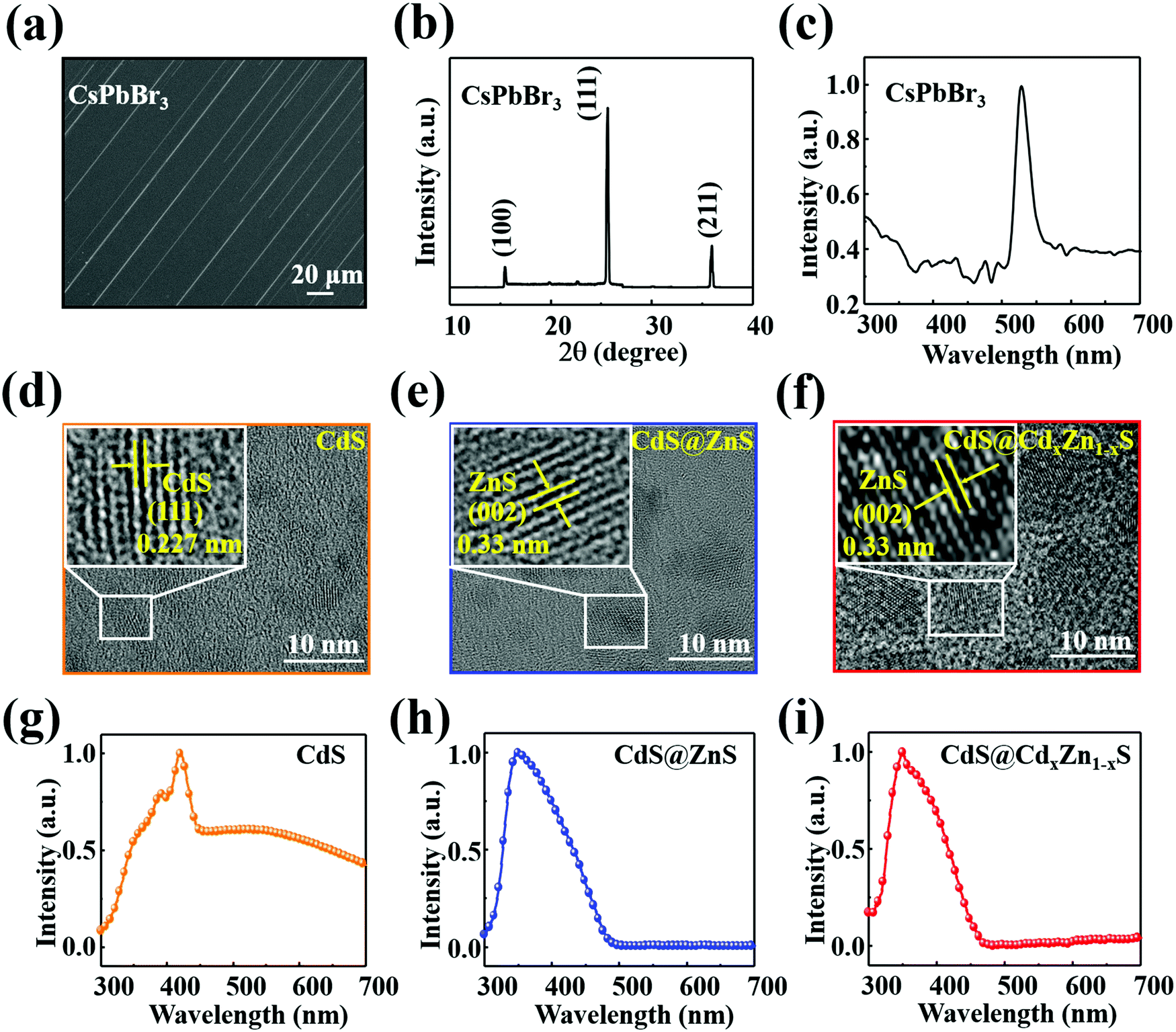 | ||
| Fig. 1 An SEM micrograph (a), the X-ray diffraction pattern (b), and the absorption spectrum (c) of CsPbBr3 NWs. TEM micrographs of CdS QDs (d), CdS@ZnS QDs (e), and CdS@CdxZn1−xS QDs (f); the corresponding insets exhibit the lattice fringe patterns of the QDs. Absorption spectrum of CdS QDs (g), CdS@ZnS QDs (h), and CdS@CdxZn1−xS QDs (i). | ||
In order to confirm the formation of heterostructures, optical microscope (OM) images, SEM images, absorption properties, EDS and the associated element mapping of the hybrid devices were obtained after spin-coating the QDs on the CsPbBr3 NWs. The OM images of the P1, P2, and P3 hybrid devices are shown in Fig. 2(a)–(c); the insets present the schematic diagram of the hybrid structure. After the QDs have been deposited on the CsPbBr3 NW, the surface of the CsPbBr3 NW becomes obfuscated and the margin is unclear, as exhibited in the SEM image (Fig. S3, ESI†). Meanwhile, the optical properties of the QDs/CsPbBr3 NW hybrid structure were investigated by steady-state absorption spectra, as shown in Fig. 2(d)–(f). Contrasting with the CsPbBr3 NW, multiple absorption bands were observed in the hybrid structure, and the typical absorption of the hybrid structure includes both QD and NW features, which confirmed that the QDs have been successfully deposited on the NW. Specifically, three obvious absorption peaks of QDs are separately located at 465 nm, 370 nm, and 365 nm, which overlapped with CsPbBr3 NWs absorption characteristics, indicating that the QDs with high absorption coefficient are promising as a photoactive layer coated on the CsPbBr3 NW to raise the photon capture ability.10,44 Moreover, the CsPbBr3 NW showed enhanced absorption after the deposition of the CdS@CdxZn1−xS QDs, which can be ascribed to the synergetic absorption of the CsPbBr3 NW and the CdS@CdxZn1−xS QDs, as shown in Fig. S4 (ESI†).10 Detailed EDS data and elemental mapping of the QDs/CsPbBr3 NW hybrid structures are shown in Fig. 2(g)–(l), which reveal the existence of Br, Pb, Cs, Cd and S elements in P1, and the presence of Br, Pb, Cs, Cd, Zn and S elements in both P2 and P3 hybrids. The atomic ratios of the basic elements of Br, Pb, Cs, Cd, and S in P1; Br, Pb, Cs, Cd, Zn, and S in P2; and Br, Pb, Cs, Cd, Zn, and S in P3 are, respectively, 59.79%, 18.40%, 18.66%, 0.81% and 2.34%; 56.34%, 16.84%, 17.88%, 1.46%, 4.96% and 2.52%; and 29.51%, 10.88%, 10.16%, 6.53%, 22.54% and 20.38%. It further demonstrates that the three QDs were satisfactorily coated on the surface of the CsPbBr3 NWs. In order to compare the diffraction peaks of the CsPbBr3 NWs before and after the QDs were decorated, the XRD of CdS@CdxZn1−xS QDs/CsPbBr3 NW has been investigated, and the patterns of both the CsPbBr3 NW and the CdS@CdxZn1−xS QDs/CsPbBr3 NW are depicted in Fig. S5 (ESI†). It is observed that the CsPbBr3 NW planes show a strong diffraction intensity, while the small diffraction peaks of the CdS@CdxZn1−xS QDs that occurred behind 40° are not obvious, which may be due to the small amount of CdS@CdxZn1−xS QDs compared with the CsPbBr3 NW. Moreover, the diffraction intensity of the CsPbBr3 NW(111) plane decreases accordingly.76
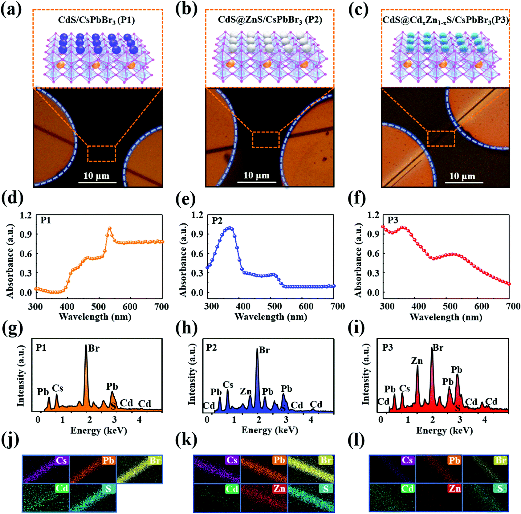 | ||
| Fig. 2 OM images of the P1 (a), P2 (b), and P3 (c) hybrid devices. Insets: Schematic diagrams of the QDs/CsPbBr3 hybrid structures. Absorption spectra of P1, P2, and P3 from 300 nm to 700 nm (d–f). EDS data (g–i) and corresponding elemental mapping images (j–l) for P1, P2, and P3. | ||
Mixed-dimensional photodetectors were fabricated based on the single CsPbBr3 NW modified with QDs, and the optoelectronic performance of the device was measured before and after QD deposition, as displayed in Fig. 3. In order to vividly demonstrate the structure of the devices, structure models of P1, P2, and P3 are depicted in Fig. 3(a), (b), and (c), respectively. Fast response to optical signals is critical for optoelectronic applications of a photodetector. Fig. 3(d)–(f) present the characteristic current versus time (I–T) curves of the photodetectors with various incident light powers ranging from 19 to 1330 μW cm−2 under a 405 nm laser at 5 V. Compared to the CsPbBr3 NW photodetector (P0), the photocurrents of P1, P2, and P3 are enhanced to different extents under light with various power densities. Among them, an extremely obvious improvement in the photoexcitation response was observed in P3. Similarly, the on/off ratio of the P3 device was also dramatically enhanced, increasing by over one order of magnitude compared to that of P0. Here, the on/off ratio is defined as Ilight/Idark, where Ilight and Idark are the photocurrent and dark current, respectively. The one cycle time-dependent photoresponse of the hybrid devices and pristine CsPbBr3 NW device are separately illustrated in Fig. 3(g)–(i) and Fig. S6 (ESI†), in which the response time is defined as the time taken from the dark current increasing to 90% of the maximum stable photocurrent, and the recovery time is the time taken to decrease to 10% of the maximum. It can be seen that the rise and decay times of P0 are 556 μs and 559 μs. After QD deposition, the rise and decay times of the P1, P2, and P3 devices respectively decreased to 290 μs/500 μs, 280 μs/480 μs and 340 μs/330 μs. As the carrier concentration increases, the photocurrent rate is increased, and the fall time decreases.45 Moreover, the 1,2-ethanedithiol (EDT) between the CsPbBr3 NW and the QDs could efficiently improve the charge-carrier transfer, resulting in the greatly shortened rise and decay times.46 Importantly, the dark and light current modulation characteristics as a function of voltage for the CsPbBr3 NW devices before and after QDs deposition are separately exhibited in Fig. 3(j) and (k). Compared with the P0 device, the dark currents in the hybrid devices were decreased while the photocurrents were strikingly increased; the QDs act as a passivation layer, which protects the CsPbBr3 NW devices and leads to the lower dark current. In addition, upon light illumination, a large amount of charge carriers are generated in the QDs and spontaneous electron transfer from the QDs to the CsPbBr3 occurs due to the field and the energy band alignment, resulting in the improved photocurrent in the hybrid devices. Remarkably, it is worth noting that the hybrid device with CdS@CdxZn1−xS QDs has the most improved photoelectric performance, whereby the photocurrent rises significantly from 0.27 nA to 5.7 nA under illumination intensity of 19 μW cm−2 at 5 V. Similarly, the I–V characteristics of the single CsPbBr3 NW and the hybrid devices under 405 nm illumination with various light intensities of 60, 161, 492, and 1330 μW cm−2 are provided in Fig. S7 (ESI†) and followed the same trends as the results in Fig. 3(k). On the basis of the above results, the photocurrent enhancement ratios of the hybrid devices relative to P0 was calculated and are exhibited in Fig. 3(l), in which the ratios of P2/P0 and P3/P0 were obviously enhanced with the increase of power density. The photocurrent was strengthened by an average factor of 1.2, 3, and 10 times after modification with the CdS QDs, CdS@ZnS QDs and CdS@CdxZn1−xS QDs, respectively. The photocurrent enhancement ratio is defined as I1/I0, I2/I0, and I3/I0, where I0, I1, I2 and I3 are the photocurrents of the P0, P1, P2, and P3 devices at 5 V, respectively. Evidently, P3 displayed the best optoelectronic performance among the hybrid devices, which may be attributed to the stronger absorption characteristics of the CdS@CdxZn1−xS QDs and the quasi-type II energy band structure, that is the funnel-shaped energy level, which can obviously facilitate the electron–hole pair separation and transfer.36
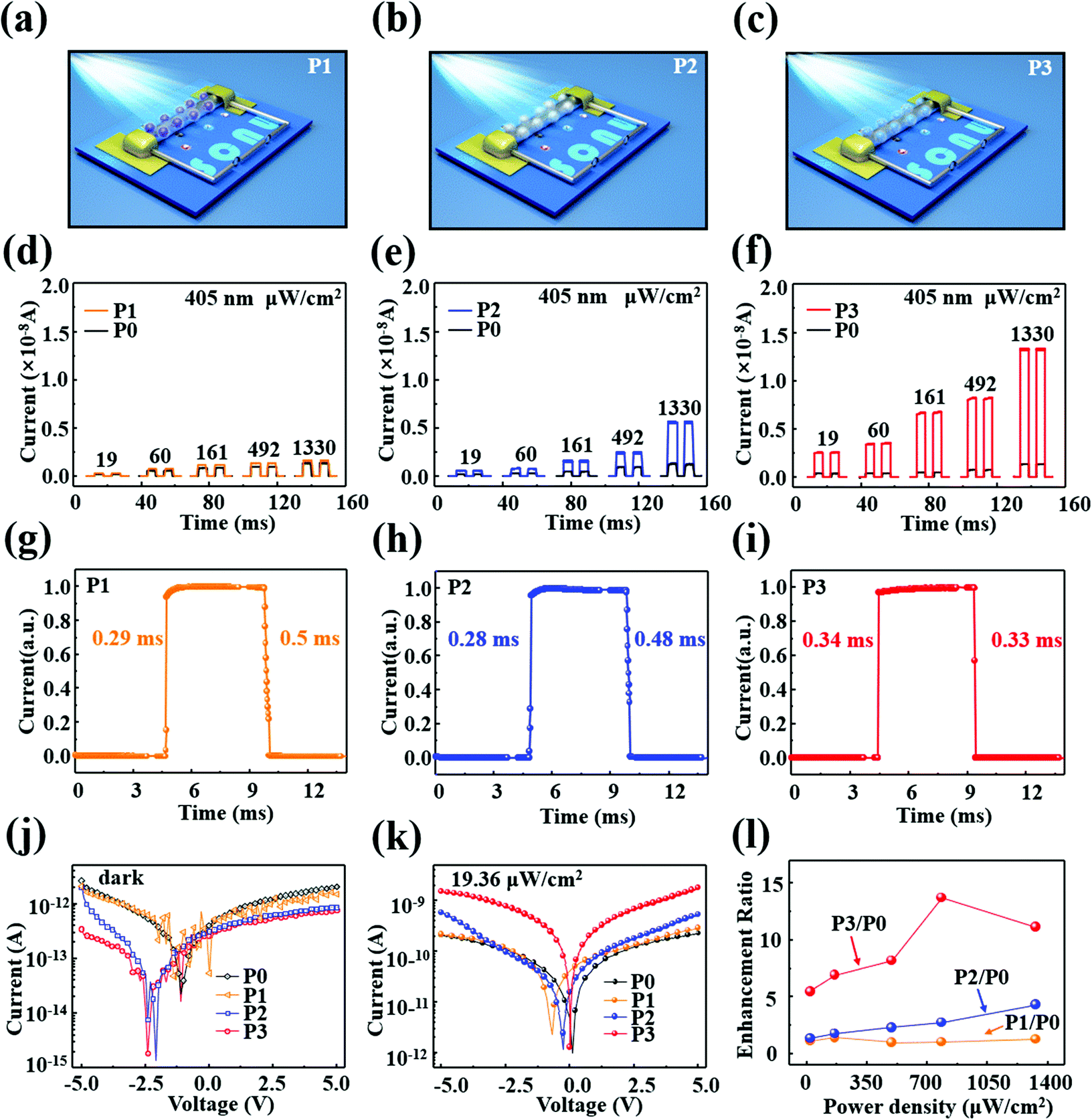 | ||
| Fig. 3 The optoelectronic performances of CsPbBr3 and hybrid devices. Schematic illustrations of the P1 (a), P2 (b), and P3 (c) hybrid devices. The I–T characteristic curves of P0 and P1 (d), P0 and P2 (e), and P0 and P3 (f) with different power densities at a voltage of 5 V. One cycle of the photoresponse under a 405 nm laser at 19 μW cm−2, estimating both the rise and fall times: the photoresponses of P1 (g), P2 (h), and P3 (i). I–V characteristics of the P0 device and P1, P2, and P3 hybrid devices without illumination (j). I–V characteristics of the P0 device and P1, P2, and P3 hybrid devices under a 405 nm laser with light intensity of 19 μW cm−2 (k). The photocurrent enhancement ratios of the P1, P2, and P3 hybrid devices compared to the P0 device (l). | ||
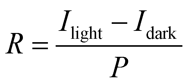
Responsivity (R) is an important parameter for the performance of a photodetector, which is calculated to better understand the role of QDs in the hybrid device performance. The value of R is defined as the ratio of the photocurrent and the incident illumination power (that is, Iph/Plight), as shown in the following formula:18,47,48
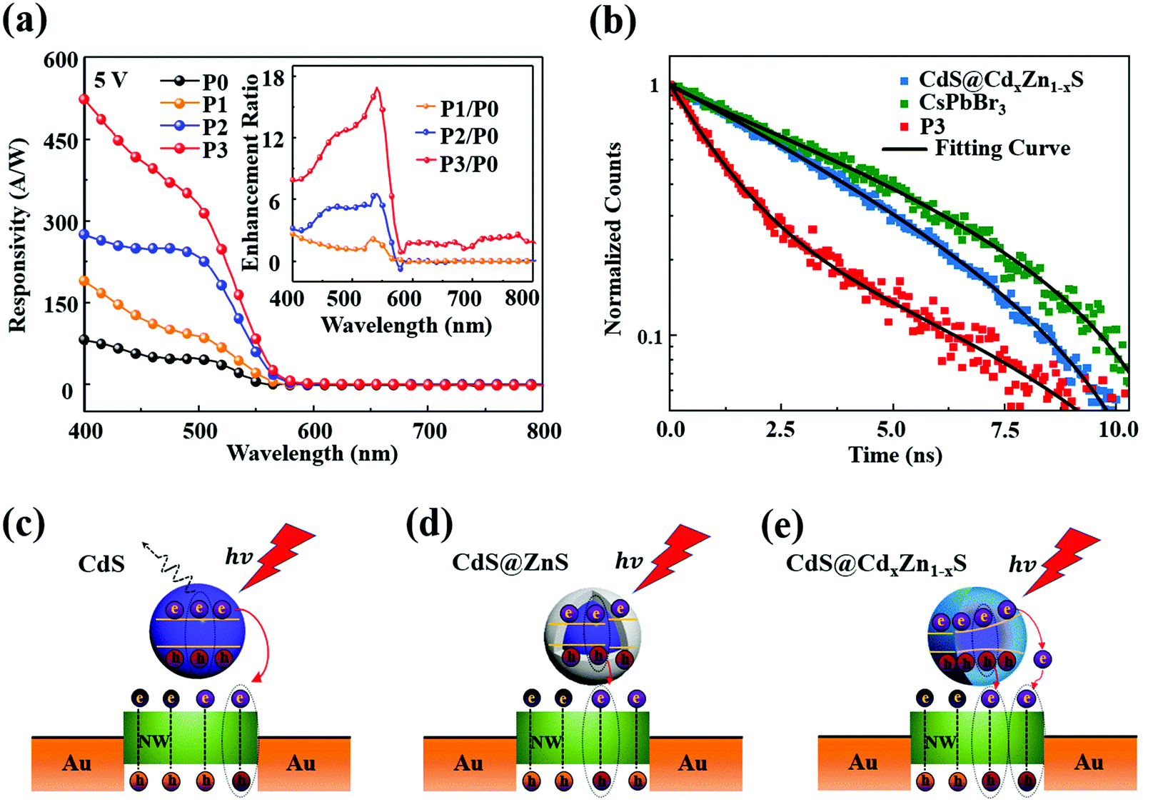 | ||
| Fig. 4 (a) Photoresponsivity of P0, P1, P2, and P3 devices at wavelengths from 400 nm to 800 nm; the inset presents the responsivity enhancement ratios of the P1, P2, and P3 devices relative to P0. (b) Time-resolved PL decay curves of the pure CsPbBr3 NWs, the CdS@CdxZn1−xS QDs, and the CsPbBr3 NWs after CdS@CdxZn1−xS QD deposition. (c–e) Schematic diagrams of the channel current transport mechanism and energy band diagram of the P1, P2, and P3 hybrid devices, respectively, upon illumination. | ||
To further understand the charge-carrier generation and transfer mechanism, steady-state photoluminescence (PL) spectra and time-resolved PL (TRPL) spectra were employed in comparison of pristine and hybrid systems. As shown in Fig. S10(a) and (b) (ESI†), pure CsPbBr3 and CdS@CdxZn1−xS QDs exhibit PL emissions centered around 527 nm and 470 nm, respectively. After formation of the heterostructure between CsPbBr3 and CdS@CdxZn1−xS QDs, the PL intensities both increased significantly. Additionally, the TRPL decay curves of the pure CsPbBr3, pure CdS@CdxZn1−xS QDs and P3 are shown in Fig. 4(b). As illustrated in Table S1 (ESI†), monoexponential decay is required to fit the pure CsPbBr3 NW and CdS@CdxZn1−xS QDs with a single lifetime value of 7.078 ns and 5.093 ns, respectively, which can be ascribed to the exciton recombination (τ1). For the P3 hybrid structure, bi-exponential functions are necessary to fit the decay curves, and the two components can be linked to exciton recombination (τ1 = 1.158 ns) and free-carrier recombination (τ2 = 6.429 ns); A1 and A2 are the relative amplitudes of the lifetimes, respectively.49,50 Specifically, the rate of exciton recombination decay for the CsPbBr3 NWs and the CdS@CdxZn1−xS QDs was reduced by 60% with the free-carrier lifetime of 6.429 ns for the P3 device. The suppressed exciton recombination and shorter lifetime indicate exciton dissociation at the CdS@CdxZn1−xS QDs/CsPbBr3 NW interface, and effective photogenerated charge separation, which is beneficial for the charge carriers transferred from QDs to NW through strongly inhibiting exciton recombination.51,52 At the same time, the transfer of electrons from the QDs to the NW leaving holes in the QDs leads to increased free-carrier PL emission, which is consistent with our observations in Fig. S10(a) and (b) (ESI†). Based on the presented results, the performance improvement of the CsPbBr3 NW photodetectors optimized by gradient-alloyed QDs under the same conditions is always better than that of binary QDs and core/shell QDs.
According to previous studies,36,41,53 the only differences among the three types of QDs are the energy band structure and the energy level alignment of the QDs/CsPbBr3 NW hybrid devices, as shown in Fig. 4(c)–(e). For P1 (Fig. 4c), the photons are absorbed by the CdS QDs, to generate the electron–hole pairs, and the electrons can transfer from the QDs to the CsPbBr3 NW owing to the high carrier mobility of the CsPbBr3 and the band energy alignment, which can be achieved to enhance the photoelectric efficiency.54 However, the simple band structure of binary QDs relative to core/shell and alloyed QDs easily promoted the electron–hole recombination, which can obviously inhibit the charge-carrier separation and transfer to NWs. By contrast, as shown in Fig. 4(d), the CdS@ZnS core/shell QDs may favor effective electron–hole pair separation due to the heterojunction being composed of the core and shell, but the lattice mismatch between the core and shell facilitates charge-carrier recombination and acts as a barrier against the charge transfer from the QDs to the NW.55 Finally, the electrons and holes easily concentrate and recombine in the boundary, resulting in a decrease in the carrier concentration.55,56 In principle, the nonradiative energy transfer plays an important role between the QDs and the NW.55 First, excitons generated in the photosensitive layer are transferred to CsPbBr3 NW via nonradiative dipole–dipole coupling, and then electron–hole pairs are generated in the CsPbBr3 NW, thereby enhancing the performance of the device.55,57 For the CdS@CdxZn1−xS QDs, the alloying from the inside to outside without any boundary and mismatch makes their electronic structure convert from Type I to quasi-Type II, which facilitates the rapid separation of electron–hole pairs.40 The special funnel-shaped energy level structure expands the light absorption range because the opening gradually increases, facilitating electron tunneling so that a large number of carriers can be transferred from the photosensitive CdS@CdxZn1−xS QDs layer to the CsPbBr3 NW transport layer, as shown in Fig. 4(e). At the same time, nonradiative energy transfer is also working.
Furthermore, the EQE and D* represent the ability of a photodetector to detect signals, which are significant parameters and are calculated according to the following equations:48,58
where h is Planck's constant (6.62606896(33) × 10−34), c is the velocity of light, e is the elementary charge, and λ represents the wavelength of the light source. Fig. 5(a) and (b) show the R, EQE and D of the pristine and hybrid devices under an illumination intensity of 19 μW cm−2 and a voltage of 5 V. The devices decorated with QDs not only present excellent photo-responses, but also provide high external quantum efficiency and detectivity. The optical responsivity of the hybrid photodetector increased more significantly than that of the P0 device, indicating a better and more stable photosensitivity behavior after QD deposition. Among them, the R of the P3 hybrid device has been obviously enhanced, being about 10 times higher than that of the P0 device. Moreover, under the same radiation intensity and bias voltage, the D* of the P0 and P1, P2, P3 devices have maximum values of 0.92 × 10¹² and 1.73 × 10¹² Jones, 2.22 × 10¹² Jones, 1.62 × 10¹³ Jones, respectively. Compared with the P0 photodetector, the P3 hybrid structure presents at least one order of magnitude increase in detectivity and EQE from 0.92 × 10¹² to 1.62 × 10¹³ Jones and 358.87% to 4400%, respectively. Combining Fig. 5(a), (b) and Fig. S11 (ESI†) shows that the comprehensive modulation characteristic as a function of R, EQE and D is enhanced with increasing voltage, and decreases with increasing applied light intensity, where the voltage is varied from 1 V to 4 V and the light intensity is varied from 60 to 1330 μW cm−2, which indicate that the devices present excellent performance under light intensity of 19 μW cm−2 and voltage of 5 V. The performance comparison of our CsPbBr3 NW-based devices and other typically reported pure CsPbBr3 or decorated photodetectors is shown in Fig. 5(c).13,15,28,38,46,59–61,66,67,69,71–73 The detailed performances of related photodetector devices are listed in Table S2 (ESI†). Compared with the most carefully designed individual CsPbBr3 wire and hybrid photodetectors, the performance of our photodetectors modified with QDs has remarkable advantages. According to the above results, the optoelectrical performance of the CsPbBr3 NW-based photodetectors is well enhanced after modification with the CdS@CdxZn1−xS gradient-alloyed QDs, which provides an efficient strategy for research on high-performance miniature 0D–1D mixed-dimensional photodetectors and promotes the application of gradient-alloyed QDs in NW-based photodetectors.
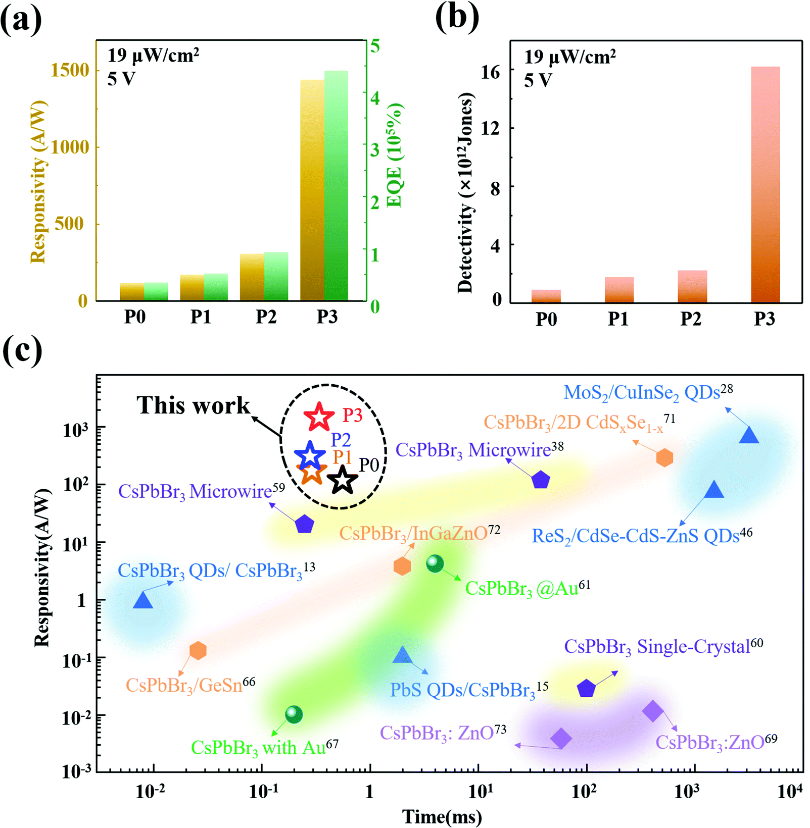 | ||
| Fig. 5 Photoresponsivity, EQE (a), and specific detectivity (b) data for P0, P1, P2, and P3 devices at a light intensity of 19 μW cm−2 and a voltage of 5 V. A comparison of the responsivities and response times of CsPbBr3-based photodetectors (c). | ||
Conclusions
In conclusion, CsPbBr3 NW photodetectors decorated with individual CdS QDs, CdS@ZnS core–shell QDs, and gradient-alloyed CdS@CdxZn1−xS QDs were investigated systematically. It was demonstrated that although the binary CdS QDs, CdS@ZnS core–shell QDs, and gradient-alloyed CdS@CdxZn1−xS QDs could all induce an enhancement of the photocurrent of the CsPbBr3 NW photodetector, the gradient-alloyed CdS@CdxZn1−xS QDs exhibited the best performance improvement. Specifically, the responsivity of the CsPbBr3 NW photodetector was enhanced about 10-fold, reaching 1442 A W−1 under 405 nm laser illumination, and the rise and decay times of the time-dependent photoresponse were reduced from 556 μs and 559 μs to 340 μs and 330 μs, respectively. The excellent comprehensive optoelectrical performance of the CdS@CdxZn1−xS QDs/CsPbBr3 NW hybrid photodetector benefits from the strong light absorption abilities and fast photoexcited electron–hole pair separation properties of gradient-alloyed quasi-type II CdS@CdxZn1−xS QDs, which possess a unique typical funnel-shaped energy structure. This work not only proposes a novel strategy for obtaining perovskite-based mixed-dimensional photodetectors with satisfactory performance, but it also provides new insight into the photoelectric conversion process of gradient-alloyed QDs, which should inspire many future investigations into gradient-alloyed QD-based photodetectors.Experimental
CVD growth of CsPbBr3 NWs
The directional CsPbBr3 NWs were grown on a mica substrate using the CVD method in a tube furnace. During the growth process, a mixture of lead(II) bromide (PbBr2, 99.99%) and cesium bromide (CsBr, 99.99%) powders (molar ratio 1![[thin space (1/6-em)]](https://www.rsc.org/images/entities/char_2009.gif) :2) was placed into an Al2O3 boat as the precursor. A fluorophlogopite mica [KMg3(AlSi3O10)F2] sheet with (001) was cleaved to a thin sheet as the growth substrate. The fresh surface was placed downstream of the Al2O3 boat at a distance of 4 cm away from the precursor. The reactor temperature was 570 °C and the chamber pressure was maintained at ∼2 torr by the Ar carrier flow of 100 standard cubic centimeters per minute (sccm). The growth was maintained for 5 minutes, after which the furnace naturally cooled to room temperature.
:2) was placed into an Al2O3 boat as the precursor. A fluorophlogopite mica [KMg3(AlSi3O10)F2] sheet with (001) was cleaved to a thin sheet as the growth substrate. The fresh surface was placed downstream of the Al2O3 boat at a distance of 4 cm away from the precursor. The reactor temperature was 570 °C and the chamber pressure was maintained at ∼2 torr by the Ar carrier flow of 100 standard cubic centimeters per minute (sccm). The growth was maintained for 5 minutes, after which the furnace naturally cooled to room temperature.
Synthesis of CdS@CdxZn1−xS gradient-alloyed QDs
128.4 mg of cadmium oxide (CdO, 99.99%, 1 mmol) and 1651.3 mg (9 mmol) of zinc acetate (Zn(acet)2, 99%) were dissolved in 8 mL of oleic acid (OA, 90%) and 15 mL of 1-octadecene (ODE, 90%) to form Zn-oleate and Cd-oleate precursor 1. 51.2 mg and 384 mg of sulfur (S, 99.5%) powder (1.6 mmol) were respectively dissolved in 3 mL ODE and 6 ml of trioctylphosphine (TOP, 90%) to form S precursor 1 and precursor 2. 77.1 mg of CdO (0.6 mol) was dissolved in 0.9 mL of OA and 8.1 mL of ODE to form Cd-oleate precursor 2. Then, Zn-oleate and Cd-oleate precursor 1 prepared in the first step was heated to 303 °C, and then all the S precursor 1 was quickly injected into the cationic precursors, leading to the rapid nucleation of CdS@CdxZn1−xS. After 20 minutes of reaction, 3 mL of S precursor 2 and 6 mL of Cd-oleate precursor 2 were added to the reaction solution by injection pump with rates of 3 mL h−1 and 10 mL h−1, respectively. After 5 min of reaction, 2 mL of oleylamine (OAm, 90%) was injected into the flask at a temperature of 180 °C for 5 min. After the reaction, the solution was naturally cooled to room temperature. All of the synthesis process for the quantum dots is carried out under an inert gas environment. The detailed preparation processes for the CdS and CdS@ZnS QDs are depicted in the ESI.†Device fabrication and measurements
The CsPbBr3 NW photodetector with a Ni/Au electrode (10/50 nm) was fabricated using the electron beam lithography process. Then, QDs were spin-coated on the surface of the CsPbBr3 NW after testing the pristine CsPbBr3 NW-based device. The prepared QDs were first dissolved in toluene with a concentration of 30 mg mL−1, and then two drops of QDs supernatant were directly deposited onto the sample with a rotate speed of 1000 rpm, followed by three drops of EDT ligands in acetone at a rotation speed of 2000 rpm.62 The EDT solution for ligand exchange was 2 vol% in acetonitrile.46 This manipulation was repeated once. Finally, the hybrid device was dried on heating equipment at 60 °C for 30 mins to remove residual organic solvents.63 In this work, we spin-coated three types of QDs, namely CdS QDs, CdS@ZnS QDs, and CdS@CdxZn1−xS QDs. Then, in order to facilitate the charge-carrier transport from the QDs to the NW, it was necessary to exchange long ligands with short ligands.Characterization
The sample quality and morphology were characterized by XRD, TEM, and SEM combined with EDS. All optical measurements were performed using a picosecond laser, microscopy equipment, and a spectrometer integrated with time-correlated single photon counting (TCSPC) detection. Electric and photoresponse measurements of the devices were conducted under an ambient atmosphere using a three-probe station (Keithley Agilent B2902A system) with a multi-wavelength optical-fiber laser, a computer-controlled measurement system with a Stanford SRS low-noise current preamplifier (SR570)/SRS low-noise voltage preamplifier (SR560) in conjunction with a GPIB controller (GPIBUSB-HS, NI 488.2), and a four-probe station (PSAICPB6A, Precision Systems Industrial Co., Ltd) equipped with a Keithley B2636B semiconductor source meter. The photoresponse behavior of the device was tested by using a 405 nm optical-fiber laser.Conflicts of interest
The authors declare no conflicts of interest.Acknowledgements
This work received financial support from the National Natural Science Foundation of China (22102058, 61874037), Guangdong Basic and Applied Basic Research Foundation (2022A1515011242), Natural Science Foundation of Guangdong Province (2018030310031), Science and Technology Program of Guangzhou (202102021121, 202103030001), the Open Research Fund of Songshan Lake Materials Laboratory (2021SLABFN01), Science and Technology Program of Guangzhou (202103030001), and the Outstanding Young Talent Project of South China Normal University.References
- F. P. García de Arquer and E. H. Sargent, Nat. Electron., 2018, 1, 380–381 CrossRef.
- A. M. Morales and C. M.-J. S. Lieber, Science, 1998, 279, 208 CrossRef CAS PubMed.
- Z. L. Wang, Mater. Sci. Eng., R, 2009, 64, 33 CrossRef.
- Z. Zheng, F. Zhuge, Y. Wang, J. Zhang, L. Gan, X. Zhou, H. Li and T. Zhai, Adv. Funct. Mater., 2017, 27, 1703115 CrossRef.
- H. Chen, H. Liu, Z. Zhang, K. Hu and X. Fang, Adv. Mater., 2016, 28, 403 CrossRef CAS PubMed.
- H. Chen, K. Liu, L. Hu, A. A. Al-Ghamdi and X. Fang, Mater. Today, 2015, 18, 493 CrossRef CAS.
- J. He, H. Chen, Q. Zhao, Y. Wang, Y. Pan, S. Huang, F. C. C. Ling, S. Wang and S. Su, J. Mater. Chem. C, 2021, 9, 9484 RSC.
- M. M. Lee, J. Teuscher, T. Miyasaka, T. N. Murakami and H. J. Snaith, Science, 2012, 338, 643 CrossRef CAS PubMed.
- S. Goniszewski, M. Adabi, O. Shaforost, S. M. Hanham, L. Hao and N. J.-S. R. Klein, Sci. Rep., 2016, 6, 22858 CrossRef CAS PubMed.
- X. Peng, Y. Guo, Q. Yin, J. Wu and Y. Xie, J. Am. Chem. Soc., 2017, 139, 5242 CrossRef CAS PubMed.
- B. Yang, F. Zhang, J. Chen, S. Yang, X. Xia, T. Pullerits, W. Deng and K. Han, Adv. Mater., 2017, 29, 1703751 Search PubMed.
- F. Hu, H. Zhang, C. Sun, C. Yin, B. Lv, C. Zhang, W. W. Yu, X. Wang, Y. Zhang and M. Xiao, ACS Nano, 2015, 9, 12410 CrossRef CAS PubMed.
- S. Yan, S. Tang, M. Luo, L. Xue, S. Liu, E. E. Elemike, B. S. Bae, J. Akram, J. Chen, Z. Zhao, Z. Zhu, X. Zhang, W. Lei and Q. Li, J. Mater. Chem. C, 2021, 9, 10089 RSC.
- Y. T. Yoo, D. Y. Heo, S. R. Bae, J. Park, T. W. Lee, H. W. Jang, S. H. Ahn and S. Y. Kim, Small Methods, 2021, 5, 2100054 CrossRef CAS PubMed.
- J. Navarro Arenas, A. Soosaimanickam, H. Pashaei Adl, R. Abargues, P. P. Box, P. J. Rodriguez-Canto and J. P. Martinez-Pastor, Nanomaterials, 2020, 10, 1297 CrossRef PubMed.
- Y. Zheng, M. Jiang, L. Guo, G. Hu, Y. Gu, J. Xi, Z. Huo, F. Ll, S. Wang and C. Pan, Nano Energy, 2021, 85, 105951 CrossRef.
- B. Liu, R. R. Gutha, B. Kattel, M. Alamri, M. Gong, S. M. Sadeghi, W. L. Chan and J. Z. Wu, ACS Appl. Mater. Interfaces, 2019, 11, 32301 CrossRef CAS PubMed.
- K. Hu, H. Chen, M. Jiang, F. Teng, L. Zheng and X. Fang, Adv. Funct. Mater., 2016, 26, 6641 CrossRef CAS.
- M. Dai, H. Chen, R. Feng, W. Feng, Y. Hu, H. Yang, G. Liu, X. Chen, J. Zhang, C. Y. Xu and P. Hu, ACS Nano, 2018, 12, 8739 CrossRef CAS PubMed.
- M. Dai, H. Chen, F. Wang, Y. Hu, S. Wei, J. Zhang, Z. Wang, T. Zhai and P. Hu, ACS Nano, 2019, 13, 7291 CrossRef CAS PubMed.
- M. L. Lu, C. W. Lai, H. J. Pan, C. T. Chen, P. T. Chou and Y. F. Chen, Nano Lett., 2013, 13, 1920 CrossRef CAS PubMed.
- L. Li, Z. Lou and G. Shen, Adv. Funct. Mater., 2017, 28, 1705389 CrossRef.
- Y. Zhang, J. Guo, Y. Xu, W. Huang, C. Li, L. Gao, L. Wu, Z. Shi, C. Ma, Y. Ge, X. Zhang and H. Zhang, Nanoscale Horiz., 2020, 5, 847–856 RSC.
- S. Zhang, X. Wang, Y. Chen, G. Wu, Y. Tang, L. Zhu, H. Wang, W. Jiang, L. Sun, T. Lin, H. Shen, W. Hu, J. Ge, J. Wang, X. Meng and J. Chu, ACS Appl. Mater. Interfaces, 2019, 11, 23667 CrossRef CAS PubMed.
- T. Yu, F. Wang, Y. Xu, L. Ma, X. Pi and D. Yang, Adv. Mater., 2016, 28, 4912 CrossRef CAS PubMed.
- F. Li, D. Benetti, M. Zhang, J. Feng, Q. Wei and F. Rosei, Small Methods, 2021, 5, 2100109 CrossRef CAS PubMed.
- D. Xie, L. Wei, M. Xie, L. Jiang, J. Yang, J. He and J. Jiang, Adv. Funct. Mater., 2021, 31, 2010655 CrossRef CAS.
- T. Shen, F. Li, Z. Zhang, L. Xu and J. Qi, ACS Appl. Mater. Interfaces, 2020, 12, 54927 CrossRef CAS PubMed.
- K. Shen, X. Li, H. Xu, M. Wang, X. Dai, J. Guo, T. Zhang, S. Li, G. Zou, K. L. Choy, I. P. Parkin, Z. Guo, H. Liu and J. Wu, J. Mater. Chem. A, 2019, 7, 6134 RSC.
- T. Bi, J. Yao, Z. Chen, Z. Du, H. Liu, H. He, X. Shen and Y. Fu, J. Mater. Sci.: Mater. Electron., 2022, 33, 5997 CrossRef CAS.
- Y. J. Hsiao, L.-W. Ji, H.-Y. Lu, T.-H. Fang and K.-H. Hsiao, IEEE Sens. J., 2017, 17, 3710 CAS.
- K. Boldt, S. Bartlett, N. Kirkwood and B. J.-N. L. Johannessen, Nano Lett., 2020, 20, 1009 CrossRef CAS PubMed.
- L. K. Sagar, G. Bappi, A. Johnston, B. Chen, P. Todorovic, L. Levina, M. I. Saidaminov, F. P. García de Arquer, D. H. Nam, M. J. Choi, S. Hoogland, O. Voznyy and E. H. Sargent, Chem. Mater., 2020, 32, 7703 CrossRef CAS.
- W. K. Bae, L. A. Padilha, Y. S. Park, H. Mcdaniel, I. Robel, J. M. Pietryga and V. I. Klimov, ACS Nano, 2013, 7, 3411 CrossRef CAS PubMed.
- H. Cui, Z. Liang, X. Lu, Y. Tong, C. Su, H. Liu and J. Shi, Energy Environ. Sci., 2011, 4, 466 RSC.
- X. Liu, D. Wen, Z. Liu, J. Wei, D. Bu and S. Huang, Chem. Eng. J., 2020, 402, 126178 CrossRef CAS.
- Z. Dan, C. Wang, W. Gao, K. Shu, L. Wu, W. Wang, Q. Zhao, X. Liu, X. Liu, N. Huo and J. Li, APL Mater., 2021, 9, 081117 CrossRef CAS.
- P. Gui, Z. Chen, B. Li, F. Yao, X. Zheng, Q. Lin and G. Fang, ACS Photonics, 2018, 5, 2113 CrossRef CAS.
- Z. Liao, Z. Xiao, Q. Li, Y. Miao, Y. Wei, H. Gu, X. Jiang, Q. Wang and J. Li, J. Phys. Chem. C, 2020, 124, 24315 CrossRef CAS.
- X. Ying, Y. Liu, Z. Liu, M. Zhang, C. Wang, W. Wang, H. Gu, R. Huang, D. Luo and X. J.-C. S. Liu, Catal. Sci. Technol., 2021, 11, 5917 RSC.
- D. Chen, F. Zhao, H. Qi, M. Rutherford and X. Peng, Chem. Mater., 2010, 22, 1437 CrossRef CAS.
- M. Shoaib, X. Zhang, X. Wang, H. Zhou, T. Xu, X. Wang, X. Hu, H. Liu, X. Fan, W. Zhang, T. Yang, S. Yang, S. Yang, Q. Zhang, X. Zhu, L. Sun and A. Pan, J. Am. Chem. Soc., 2017, 139, 15592 CrossRef CAS PubMed.
- Y. Wang, X. Sun, R. Shivanna, Y. Yang, Z. Chen, Y. Guo, G. C. Wang, E. Wertz, F. Deschler, Z. Cai, H. Zhou, T. M. Lu and J. Shi, Nano Lett., 2016, 16, 7974 CrossRef CAS PubMed.
- S. Cai, X. Xu, W. Yang, J. Chen and X. Fang, Adv. Mater., 2019, 31, 1808138 CrossRef PubMed.
- M. Li, J. S. Chen, P. K. Routh, P. Zahl, C. Y. Nam and M. Cotlet, Adv. Funct. Mater., 2018, 28, 1707558 CrossRef.
- J. K. Qin, D. D. Ren, W. Z. Shao, Y. Li, P. Miao, Z. Y. Sun, P. A. Hu, L. Zhen and C. Y. Xu, ACS Appl. Mater. Interfaces, 2017, 9, 39456 CrossRef CAS PubMed.
- W. Zheng, F. Huang, R. Zheng and H. Wu, Adv. Mater., 2015, 27, 3921 CrossRef CAS PubMed.
- X. Liu, L. Gu, Q. Zhang, J. Wu, Y. Long and Z. Fan, Nat. Commun., 2014, 5, 4007 CrossRef CAS PubMed.
- D. Yang, R. Yang, K. Wang, C. Wu, X. Zhu, J. Feng, X. Ren, G. Fang, S. Priya and S. F. Liu, Nat. Commun., 2018, 9, 3239 CrossRef PubMed.
- L. Wang, L. Fu and L. Yin, Sol. RRL, 2020, 4, 2000417 CrossRef CAS.
- H. Huang, H. Yuan, K. Janssen, G. Solís-Fernández, Y. Wang, C. Y.-X. Tan, D. Jonckheere, E. Debroye, J. Long, J. Hendrix, J. Hofkens, J. A. Steele and M. B.-J. Roeffaers, ACS Energy Lett., 2018, 3, 755 CrossRef CAS.
- K. Zheng, K. Zidek, M. Abdellah, M. E. Messing, M. J.-A. Marri and T. Pullerits, J. Phys. Chem. C, 2016, 120, 3077 CrossRef CAS.
- K. Boldt, N. Kirkwood, G. A. Beane and P. Mulvaney, Chem. Mater., 2013, 25, 4731 CrossRef CAS.
- Y. Song, N. Li, D. Chen, Q. Xu, H. Li, J. He and J. Lu, Appl. Catal., B, 2018, 238, 255 CrossRef CAS.
- A. Raja, A. M. Castillo, J. Zultak, X. X. Zhang, Z. Ye, C. Roquelet, D. A. Chenet, A. M. Van Der Zande, P. Huang, S. Jockusch, J. C. Hone, D. R. Reichman, L. E. Brus and T. F. Heinz, Nano Lett., 2016, 16, 2328 CrossRef CAS PubMed.
- C. W. Raubach, Y. V.-B. D. Santana, M. M. Ferrer, P. G.-C. Buzolin, J. R. Sambrano and E. Longo, Dalton Trans., 2013, 42, 11111 RSC.
- K. M. Goodfellow, C. Chakraborty, K. Sowers, P. Waduge, M. Wanunu, T. Krauss, K. Driscoll and A. N. Vamivakas, Appl. Phys. Lett., 2016, 108, 021101 CrossRef.
- Z. Lian, Q. Yan, Q. Lv, Y. Wang, L. Liu, L. Zhang, S. Pan, Q. Li, L. Wang and J. L. Sun, Sci. Rep., 2015, 5, 16563 CrossRef PubMed.
- Y. Yang, F. Gao, Q. Liu, J. Dong, D. Li, X. Luo, J. Guo, J. Shi, Y. Lin, W. Song, X. Wang and S. Li, J. Phys. Chem. Lett., 2020, 11, 7224 CrossRef CAS PubMed.
- J. Ding, S. Du, Z. Zuo, Y. Zhao, H. Cui and X. Zhan, J. Phys. Chem. C, 2017, 121, 4917 CrossRef CAS.
- Z. Yang, M. Jiang, L. Guo, G. Hu, Y. Gu, J. Xi, Z. Huo, F. Li, S. Wang and C. Pan, Nano Energy, 2021, 85, 105951 CrossRef CAS.
- G. Konstantatos, M. Badioli, L. Gaudreau, J. Osmond and F. J.-N. N. Koppens, Nat. Nanotechnol., 2012, 7, 363 CrossRef CAS PubMed.
- J. H. Choi, A. T. Fafarman, S. J. Oh, D. K. Ko, D. K. Kim, B. T. Diroll, S. Muramoto, J. G. Gillen, C. B. Murray and C. R. J. C.-J.-o S. C. Kagan, Nano Lett., 2012, 24, 729 Search PubMed.
- F. Cao, W. Tian, K. Deng, M. Wang and L. Li, Adv. Funct. Mater., 2019, 29, 1906756 CrossRef CAS.
- X. Cheng, Y. Yuan, L. Jing, T. Zhou, Z. Li, Z. Peng, Q. Yao, J. Zhang and J. Ding, J. Mater. Chem. C, 2019, 7, 14188 RSC.
- H. Cong, X. Chu, F. Wan, Z. Chu, X. Wang, Y. Ma, J. Jiang, L. Shen, J. You and C. Xue, Small Methods, 2021, 5, 2100517 CrossRef CAS.
- Y. Dong, Y. Gu, Y. Zou, J. Song, L. Xu, J. Li, J. Xue, X. Li and H. Zeng, Small, 2016, 12, 5622 CrossRef CAS PubMed.
- W. Hu, H. Cong, W. Huang, Y. Huang, L. Chen, A. Pan and C. Xue, Light: Sci. Appl., 2019, 8, 106 CrossRef PubMed.
- C. Li, C. Han, Y. Zhang, Z. Zang, M. Wang, X. Tang and J. Du, Sol. Energy Mater. Sol. Cells, 2017, 172, 341 CrossRef CAS.
- J. Liu, F. Liu, H. Liu, J. Yue, J. Jin, J. Impundu, H. Liu, Z. Yang, Z. Peng, H. Wei, C. Jiang, Y. J. Li, L. Xie and L. Sun, Nano Today, 2021, 36, 101055 CrossRef CAS.
- M. Peng, Y. Ma, L. Zhang, S. Cong, X. Hong, Y. Gu, Y. Kuang, Y. Liu, Z. Wen and X. Sun, Adv. Funct. Mater., 2021, 31, 2105051 CrossRef CAS.
- M. Sun, Q. Fang, Z. Zhang, D. Xie, Y. Sun, J. Xu, W. Li, T. Ren and Y. Zhang, ACS Appl. Mater. Interfaces, 2018, 10, 7231 CrossRef CAS PubMed.
- P. Tang, S. Yang, J. Hu, Z. Zhang, Y. Jiang, M. Sulaman, L. Tang and B. Zou, J. Alloys Compd., 2021, 896, 163022 CrossRef.
- M. Wang, W. Tian, F. Cao, M. Wang and L. Li, Adv. Funct. Mater., 2020, 30, 1909771 CrossRef CAS.
- W. Zheng, X. Xiong, R. Lin, Z. Zhang, C. Xu and F. Huang, ACS Appl. Mater. Interfaces, 2018, 10, 1865 CrossRef CAS PubMed.
- Q. Nie, L. Yang, C. Cao, Y. Zeng, G. Wang, C. Wang and S. Lin, Chem. Eng. J., 2017, 325, 151–159 CrossRef CAS.
Footnotes |
| † Electronic supplementary information (ESI) available. See DOI: https://doi.org/10.1039/d2nh00149g |
| ‡ Ying Wei and Xiao Liu contributed equally to this work. |
| This journal is © The Royal Society of Chemistry 2022 |